
Figures & data
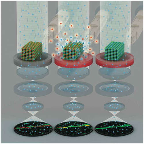
Figure 1. (a) Tip of an in situ heating furnace-based holder. The dark ring is the furnace, and the hole at its center is the slot where the TEM grid should be inserted and clamped; (b) Graphical representation of a typical heating MEMS. Panels with increasing magnification are used to highlight the position of the small electron-transparent zones. Adapted with permission from [Citation7].
![Figure 1. (a) Tip of an in situ heating furnace-based holder. The dark ring is the furnace, and the hole at its center is the slot where the TEM grid should be inserted and clamped; (b) Graphical representation of a typical heating MEMS. Panels with increasing magnification are used to highlight the position of the small electron-transparent zones. Adapted with permission from [Citation7].](/cms/asset/b01ba86b-ee12-459d-a6b8-b8995a6fda59/tapx_a_1633957_f0001_oc.jpg)
Figure 2. (a, b) Au-decorated CdSe nanorods before (a) and after (b) thermal annealing; (c-f) Isolated and interconnected Au-decorated CdSe nanorods before (c, e) and after (d, f) thermal annealing. CdSe nanorods are connected through Au domains located at the nanorods’ tips; (g, h) CdSe nanorods and Au nanocrystals before (g) and after (h) thermal annealing. After annealing, new Au domains formed at the tip of the CdSe nanorods. Reprinted with permission from [Citation28]. Copyright [2010] American Chemical Society.
![Figure 2. (a, b) Au-decorated CdSe nanorods before (a) and after (b) thermal annealing; (c-f) Isolated and interconnected Au-decorated CdSe nanorods before (c, e) and after (d, f) thermal annealing. CdSe nanorods are connected through Au domains located at the nanorods’ tips; (g, h) CdSe nanorods and Au nanocrystals before (g) and after (h) thermal annealing. After annealing, new Au domains formed at the tip of the CdSe nanorods. Reprinted with permission from [Citation28]. Copyright [2010] American Chemical Society.](/cms/asset/2e915997-e3ec-46bd-ba5c-81abdc2b673b/tapx_a_1633957_f0002_b.gif)
Figure 3. Motion and coalescence of Au domains on CdSe nanorods during annealing between 170 and 190ºC. White arrows (a-c) indicate the cluster diffusion and coalescence of two Au domains, black arrows (d) indicate the presence of flat Au/CdSe interfaces at the tip of the nanorods after annealing. Reprinted with permission from [Citation28]. Copyright [2010] American Chemical Society.
![Figure 3. Motion and coalescence of Au domains on CdSe nanorods during annealing between 170 and 190ºC. White arrows (a-c) indicate the cluster diffusion and coalescence of two Au domains, black arrows (d) indicate the presence of flat Au/CdSe interfaces at the tip of the nanorods after annealing. Reprinted with permission from [Citation28]. Copyright [2010] American Chemical Society.](/cms/asset/e13ea873-4bc1-4403-9535-fec77d8bee3c/tapx_a_1633957_f0003_b.gif)
Figure 4. Figure 4 (a) ZL image and corresponding EFTEM map (inset) of Janus-like Cu-Cu3P nanoparticles. The presence of Cu and P in the EFTEM map are indicated in red and green, respectively; (b,c) HRTEM images of Janus-like Cu-Cu3P nanoparticles characterized by two different epitaxial relationships between the Cu and Cu3P domains. Adapted with permission from [Citation29]. Copyright [2012] American Chemical Society.
![Figure 4. Figure 4 (a) ZL image and corresponding EFTEM map (inset) of Janus-like Cu-Cu3P nanoparticles. The presence of Cu and P in the EFTEM map are indicated in red and green, respectively; (b,c) HRTEM images of Janus-like Cu-Cu3P nanoparticles characterized by two different epitaxial relationships between the Cu and Cu3P domains. Adapted with permission from [Citation29]. Copyright [2012] American Chemical Society.](/cms/asset/98c7647b-60bb-4e24-a015-293c538a08c2/tapx_a_1633957_f0004_oc.jpg)
Figure 5. Effects of thermal annealing on the Janus-like nanoparticles. (a) Image of a group of nanoparticles recorded at 450ºC. Dark grey domains indicate the presence of Cu, lighter grey domains are constituted by Cu3P; (b) Image of the same group of nanoparticles after 10 min of annealing at 500ºC. No difference in tone indicating the presence of different domains can be observed; (c) HRTEM image of a Janus-like Cu-Cu3P nanoparticle annealed at 150ºC, with both domains exhibiting fcc crystal structure. Reprinted with permission from [Citation29]. Copyright [2012] American Chemical Society.
![Figure 5. Effects of thermal annealing on the Janus-like nanoparticles. (a) Image of a group of nanoparticles recorded at 450ºC. Dark grey domains indicate the presence of Cu, lighter grey domains are constituted by Cu3P; (b) Image of the same group of nanoparticles after 10 min of annealing at 500ºC. No difference in tone indicating the presence of different domains can be observed; (c) HRTEM image of a Janus-like Cu-Cu3P nanoparticle annealed at 150ºC, with both domains exhibiting fcc crystal structure. Reprinted with permission from [Citation29]. Copyright [2012] American Chemical Society.](/cms/asset/a2535fe9-b158-4659-917d-21109d5e99f9/tapx_a_1633957_f0005_b.gif)
Figure 6. (a) HRTEM image of packed CdSe/Cu3P/CdSe nano-sandwiches. The [0001] stacking of Cu3P and CdSe (individuated by the variation in electron contrast) is clearly visible; (b) EDS line profile over a HAADF-STEM image of a single nano-sandwich, showing the elemental distribution across its width; (c) HRTEM image showing the epitaxial relationship between CdSe and Cu3P at the interface of the nano-sandwich; (d) 2D-FFT patterns of the sole Cu3P and CdSe phases (labeled in red and blue, respectively) and of both phases. The combined FFT pattern highlights the structural correspondence between phases. Reprinted with permission from [Citation30]. Copyright [2013] American Chemical Society.
![Figure 6. (a) HRTEM image of packed CdSe/Cu3P/CdSe nano-sandwiches. The [0001] stacking of Cu3P and CdSe (individuated by the variation in electron contrast) is clearly visible; (b) EDS line profile over a HAADF-STEM image of a single nano-sandwich, showing the elemental distribution across its width; (c) HRTEM image showing the epitaxial relationship between CdSe and Cu3P at the interface of the nano-sandwich; (d) 2D-FFT patterns of the sole Cu3P and CdSe phases (labeled in red and blue, respectively) and of both phases. The combined FFT pattern highlights the structural correspondence between phases. Reprinted with permission from [Citation30]. Copyright [2013] American Chemical Society.](/cms/asset/6f693f18-1f02-493d-87bd-73eaf6d700ef/tapx_a_1633957_f0006_oc.jpg)
Figure 7. HRTEM images showing the thermal evolution of a single CdSe/Cu3P/CdSe nano-sandwich upon thermal annealing. (a) The initial structure is maintained from RT to 300ºC; (b) at 350ºC the CdSe cannot be observed anymore in the lateral domains and is substituted by Cu2Se domains; (c) at 400ºC even Cu3P cannot be observed anymore in the central domain and the sole Cu2Se phase can be observed in the newly formed single crystal. Scale bars correspond to 5 nm. Reprinted with permission from [Citation30]. Copyright [2013] American Chemical Society.
![Figure 7. HRTEM images showing the thermal evolution of a single CdSe/Cu3P/CdSe nano-sandwich upon thermal annealing. (a) The initial structure is maintained from RT to 300ºC; (b) at 350ºC the CdSe cannot be observed anymore in the lateral domains and is substituted by Cu2Se domains; (c) at 400ºC even Cu3P cannot be observed anymore in the central domain and the sole Cu2Se phase can be observed in the newly formed single crystal. Scale bars correspond to 5 nm. Reprinted with permission from [Citation30]. Copyright [2013] American Chemical Society.](/cms/asset/b168e06e-4f8f-4741-b32e-4d90002b6ff2/tapx_a_1633957_f0007_oc.jpg)
Figure 8. ZL images and EFTEM elemental maps of a group of nano-sandwiches recorded during a thermal annealing from RT to 400ºC and showing the progressive disappearance of P and Cd and the concomitant expansion of Cu. Scale bars correspond to 100 nm. Reprinted with permission from [Citation30]. Copyright [2013] American Chemical Society.
![Figure 8. ZL images and EFTEM elemental maps of a group of nano-sandwiches recorded during a thermal annealing from RT to 400ºC and showing the progressive disappearance of P and Cd and the concomitant expansion of Cu. Scale bars correspond to 100 nm. Reprinted with permission from [Citation30]. Copyright [2013] American Chemical Society.](/cms/asset/2af0739f-a3c9-4018-b89b-5910bcac17e9/tapx_a_1633957_f0008_oc.jpg)
Figure 9. (a, b) HRTEM images of a single Cu2Se nanoparticle at RT (a) and after thermal annealing (b). The slight variation observed in d-spacing indicates the lattice shrinking caused by thermal-activated release of Cu atoms; (c) integrated ED patterns of a Cu2Se nanoparticles at RT (magenta) and after thermal annealing (orange). The upward shift of the diffraction peaks confirms the lattice shrinking caused by the partial Cu depletion; (d) STEM image showing a group of Cu2-xSe nanoparticles. The blue rectangle indicates the area investigated by HREELS; (e, f) HREEL spectra of the area indicated in (d). No features can be observed in the spectrum recorded at RT (e), while a low-energy peak caused by a low-energy plasmon appears in the spectrum recorded after annealing; (g) DFT simulation of HREEL spectra of stoichiometric (black) and depleted (red) Cu2Se nanoparticles. The red (depleted) spectrum features a peak at the same energy as the experimental peak observed after annealing (f). Reprinted with permission from [Citation31]. Copyright [2016] American Chemical Society.
![Figure 9. (a, b) HRTEM images of a single Cu2Se nanoparticle at RT (a) and after thermal annealing (b). The slight variation observed in d-spacing indicates the lattice shrinking caused by thermal-activated release of Cu atoms; (c) integrated ED patterns of a Cu2Se nanoparticles at RT (magenta) and after thermal annealing (orange). The upward shift of the diffraction peaks confirms the lattice shrinking caused by the partial Cu depletion; (d) STEM image showing a group of Cu2-xSe nanoparticles. The blue rectangle indicates the area investigated by HREELS; (e, f) HREEL spectra of the area indicated in (d). No features can be observed in the spectrum recorded at RT (e), while a low-energy peak caused by a low-energy plasmon appears in the spectrum recorded after annealing; (g) DFT simulation of HREEL spectra of stoichiometric (black) and depleted (red) Cu2Se nanoparticles. The red (depleted) spectrum features a peak at the same energy as the experimental peak observed after annealing (f). Reprinted with permission from [Citation31]. Copyright [2016] American Chemical Society.](/cms/asset/99ee11e1-79a5-4515-9a1d-dd8f2bfe37e2/tapx_a_1633957_f0009_oc.jpg)
Figure 10. (a-d) HAADF-STEM images and EFTEM maps of Cu2Se nanospheres and CdSe nanorods at RT (a, b) and after annealing at 400ºC (c, d). Cu and Cd are indicated in green and red, respectively; (e) HRTEM image and corresponding 2D-FFT pattern of a representative hcp CdSe nanorod at RT; (f) HRTEM image and corresponding 2D-FFT pattern of the same nanorod after annealing to 400ºC. Its length is slightly diminished and its crystal structure has changed to fcc. Adapted with permission from [Citation31]. Copyright [2016] American Chemical Society.
![Figure 10. (a-d) HAADF-STEM images and EFTEM maps of Cu2Se nanospheres and CdSe nanorods at RT (a, b) and after annealing at 400ºC (c, d). Cu and Cd are indicated in green and red, respectively; (e) HRTEM image and corresponding 2D-FFT pattern of a representative hcp CdSe nanorod at RT; (f) HRTEM image and corresponding 2D-FFT pattern of the same nanorod after annealing to 400ºC. Its length is slightly diminished and its crystal structure has changed to fcc. Adapted with permission from [Citation31]. Copyright [2016] American Chemical Society.](/cms/asset/1e982886-0341-4e66-a567-5c4d503b20ba/tapx_a_1633957_f0010_oc.jpg)
Figure 11. ZL images, corresponding EFTEM elemental maps (Cu and Cd are indicated in green and red, respectively) and HRTEM images of Cu2−xSe nanoparticles and CdSe nanowires recorded at RT (a-c), 350ºC (d-f) and after annealing to 400ºC (g-i). No variation can be observed in the ZL images (a, d, g), while the diffusion of Cu and the ongoing Cu-to-Cd CE are evident from EFTEM maps (b, e, h). HRTEM images of a CdSe nanowire show its structural evolution from a hcp structure (c, RT) to a defective ((f), 350ºC) and well-defined fcc structure ((i), 400ºC). Reprinted with permission from [Citation31]. Copyright [2016] American Chemical Society.
![Figure 11. ZL images, corresponding EFTEM elemental maps (Cu and Cd are indicated in green and red, respectively) and HRTEM images of Cu2−xSe nanoparticles and CdSe nanowires recorded at RT (a-c), 350ºC (d-f) and after annealing to 400ºC (g-i). No variation can be observed in the ZL images (a, d, g), while the diffusion of Cu and the ongoing Cu-to-Cd CE are evident from EFTEM maps (b, e, h). HRTEM images of a CdSe nanowire show its structural evolution from a hcp structure (c, RT) to a defective ((f), 350ºC) and well-defined fcc structure ((i), 400ºC). Reprinted with permission from [Citation31]. Copyright [2016] American Chemical Society.](/cms/asset/7baa298c-c1aa-4438-9420-c6bd1ca0ba23/tapx_a_1633957_f0011_oc.jpg)