Figures & data
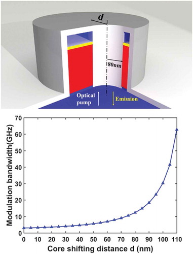
Figure 1. (a) Electrically pumped single-mode photonic crystal nano-cavity LED, reprinted from ref [Citation26] with permission; (b) Waveguide-coupled metallic nano-pillar LED on silicon, reprinted from ref [Citation8]; (c) Bowtie nano-antenna produces large single-molecule fluorescence enhancements, reprinted from ref [Citation30] with permission; (d) Plasmon nano-antenna arrays enhances light emission rate from InP MQW, reprinted from ref [Citation31] with permission.
![Figure 1. (a) Electrically pumped single-mode photonic crystal nano-cavity LED, reprinted from ref [Citation26] with permission; (b) Waveguide-coupled metallic nano-pillar LED on silicon, reprinted from ref [Citation8]; (c) Bowtie nano-antenna produces large single-molecule fluorescence enhancements, reprinted from ref [Citation30] with permission; (d) Plasmon nano-antenna arrays enhances light emission rate from InP MQW, reprinted from ref [Citation31] with permission.](/cms/asset/23c2a105-3783-439e-a06d-326f58e5c450/tapx_a_1658541_f0001_oc.jpg)
Figure 2. Theoretically predicted modulation bandwidth of nanoLEDs and nanolasers, reprinted from ref [Citation22] with permission. (a) Bulk; (b) Quantum well. The maximum modulation bandwidth is shown as a function of Q factor and the normalized effective modal volume. The color bars show the scale of modulation bandwidth with unit of GHz.
![Figure 2. Theoretically predicted modulation bandwidth of nanoLEDs and nanolasers, reprinted from ref [Citation22] with permission. (a) Bulk; (b) Quantum well. The maximum modulation bandwidth is shown as a function of Q factor and the normalized effective modal volume. The color bars show the scale of modulation bandwidth with unit of GHz.](/cms/asset/7a14cac1-09c7-4ffb-8dc6-dd88590bc259/tapx_a_1658541_f0002_oc.jpg)
Figure 3. (a) Cross-sectional view shows the structure and material stack of the electrically pumped cavity-backed slot antenna-coupled LED; (b) Top-view of the antenna-coupled LED showing extremely confined electromagnetic energy within the slot; (c) SEM picture of the fabrication antenna-coupled LED, reprinted from ref [Citation23] with permission.
![Figure 3. (a) Cross-sectional view shows the structure and material stack of the electrically pumped cavity-backed slot antenna-coupled LED; (b) Top-view of the antenna-coupled LED showing extremely confined electromagnetic energy within the slot; (c) SEM picture of the fabrication antenna-coupled LED, reprinted from ref [Citation23] with permission.](/cms/asset/38072ea8-c8b6-436b-aecb-c669ed349910/tapx_a_1658541_f0003_oc.jpg)
Figure 4. (a) Cross-sectional view, top-view and Purcell factor of metal-coated nanocylinder cavity, reprinted from ref [Citation42] with permission; (b) Schematic of nano-pillar LED on silicon substrate, calculated spontaneous emission power (coupled into the fundamental quasi-TE mode of the waveguide) as a function of the dipole wavelength, reprinted from ref [Citation8] with permission.
![Figure 4. (a) Cross-sectional view, top-view and Purcell factor of metal-coated nanocylinder cavity, reprinted from ref [Citation42] with permission; (b) Schematic of nano-pillar LED on silicon substrate, calculated spontaneous emission power (coupled into the fundamental quasi-TE mode of the waveguide) as a function of the dipole wavelength, reprinted from ref [Citation8] with permission.](/cms/asset/d88c8477-991e-442d-8f2e-9d595237c0e2/tapx_a_1658541_f0004_oc.jpg)
Figure 5. Direct current modulation of laser, reprinted from ref [Citation44] with permission.
![Figure 5. Direct current modulation of laser, reprinted from ref [Citation44] with permission.](/cms/asset/c743f3d6-7535-496d-a608-1027d032313d/tapx_a_1658541_f0005_b.gif)
Figure 6. Structure of the shifted-core coaxial nano-emitter, reprinted from ref [Citation24] with permission. (a) 3D view. The SiO2/InGaAsP/InP/SiO2 stack forms a Fabry–Pérot cavity in the vertical direction. The Ag/InGaAsP/Ag structure forms a coaxial cavity in the horizontal direction. ‘d’ denotes core-shifting distance in the y direction. (b) Cross-sectional view.
![Figure 6. Structure of the shifted-core coaxial nano-emitter, reprinted from ref [Citation24] with permission. (a) 3D view. The SiO2/InGaAsP/InP/SiO2 stack forms a Fabry–Pérot cavity in the vertical direction. The Ag/InGaAsP/Ag structure forms a coaxial cavity in the horizontal direction. ‘d’ denotes core-shifting distance in the y direction. (b) Cross-sectional view.](/cms/asset/b258aa9b-dd3f-454b-9932-8388f73713f3/tapx_a_1658541_f0006_oc.jpg)
Figure 7. (a) Q factor and resonant wavelength of the device as a function of the core-shifting distance. Inset: mode profile without shift (d = 0 nm) and at maximum shift (d = 110 nm). (b) Modulation bandwidth as a function of the core-shifting distance, reprinted from ref [Citation24] with permission. Note that the Q factor, Veff, Purcell factor and modulation bandwidth are all functions of the core shifting distance d.
![Figure 7. (a) Q factor and resonant wavelength of the device as a function of the core-shifting distance. Inset: mode profile without shift (d = 0 nm) and at maximum shift (d = 110 nm). (b) Modulation bandwidth as a function of the core-shifting distance, reprinted from ref [Citation24] with permission. Note that the Q factor, Veff, Purcell factor and modulation bandwidth are all functions of the core shifting distance d.](/cms/asset/c1ae19c3-d5b7-4930-85f3-4743a204b9a9/tapx_a_1658541_f0007_oc.jpg)
Figure 8. Far-field emission pattern of the shifted core coaxial nano-cavity, reprinted from ref [Citation24] with permission. (a) d = 0 nm; (b) d = 110 nm. Omni-directional emission can be changed to in-line bi-directional emission; (c) Evolution of emission directivity as a function of core-shifting distance.
![Figure 8. Far-field emission pattern of the shifted core coaxial nano-cavity, reprinted from ref [Citation24] with permission. (a) d = 0 nm; (b) d = 110 nm. Omni-directional emission can be changed to in-line bi-directional emission; (c) Evolution of emission directivity as a function of core-shifting distance.](/cms/asset/815af9dc-ea14-41bc-8fd8-21555e0f75c0/tapx_a_1658541_f0008_oc.jpg)
Figure 9. Threshold energy consumption at 3 V applied voltage, as a function of core-shifting distance.
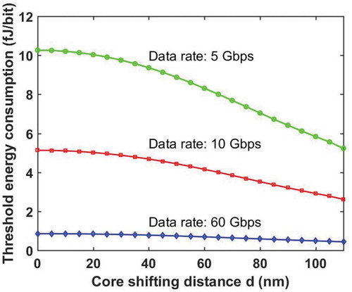
Figure 10. Energy output/bit for selected data rates and current levels.
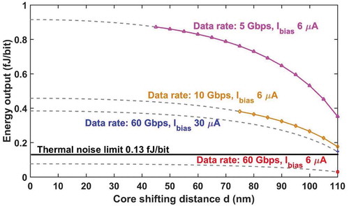
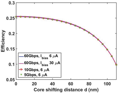
Figure 11. Device energy efficiency for selected data rates and current bias levels, as a function of core-shifting distance.