
Figures & data
Figure 1. (a) Schematic description of zero-order Bessel beams. The figure shows the conical refraction of the incoming front and the emergence of the interference pattern with the axial core and the annular features characteristic to Bessel beams. (b) Conceptual image of surface and bulk processing with Bessel pulses [Citation46]. Left: input surface pattern generated by a singe shot tightly focused ultrashort (60 fs, 14 µJ) Bessel beam () on fused silica surface; scanning electron microscope (SEM) image. The Bessel ring pattern is recognizable. Right: Back surface (exit surface) nanoscale structure in fused silica induced by a single shot moderately-focused ps stretched laser pulse (5 ps, 14 µJ,
); SEM image. (c) Example of sub-100 nm structures achieved by tightly focused Bessel beams in volume glasses [Citation46]. Transverse morphology features involving direct volume focusing of ultrafast (60 fs) Bessel beams of higher angle (
).
![Figure 1. (a) Schematic description of zero-order Bessel beams. The figure shows the conical refraction of the incoming front and the emergence of the interference pattern with the axial core and the annular features characteristic to Bessel beams. (b) Conceptual image of surface and bulk processing with Bessel pulses [Citation46]. Left: input surface pattern generated by a singe shot tightly focused ultrashort (60 fs, 14 µJ) Bessel beam (θair=22∘) on fused silica surface; scanning electron microscope (SEM) image. The Bessel ring pattern is recognizable. Right: Back surface (exit surface) nanoscale structure in fused silica induced by a single shot moderately-focused ps stretched laser pulse (5 ps, 14 µJ, θglass≃8∘); SEM image. (c) Example of sub-100 nm structures achieved by tightly focused Bessel beams in volume glasses [Citation46]. Transverse morphology features involving direct volume focusing of ultrafast (60 fs) Bessel beams of higher angle (θglass≃15∘).](/cms/asset/4ea16d95-af00-4693-8456-44e83969fb83/tapx_a_1659180_f0001_oc.jpg)
Figure 2. (a) Examples of glass parts cleaved and cut by non-diffractive Bessel beams. (b) Images of resulting surface and side walls (courtesy of K. Mishchik, Amplitude Systems [Citation57]). (c) A Bragg gratings waveguide fabricated by a combination of Gauss and Bessel beam irradiation [Citation70]. The figure shows the transmitted mode (d). An electron microscopy image of the nanostructured range is given (e). (f) Resonant Bragg optical transmission spectrum in the telecom range. (g) Examples of embedded waveguides with Bessel nano-scatterers sampling electric fields for reconstructing spectral information [Citation71].
![Figure 2. (a) Examples of glass parts cleaved and cut by non-diffractive Bessel beams. (b) Images of resulting surface and side walls (courtesy of K. Mishchik, Amplitude Systems [Citation57]). (c) A Bragg gratings waveguide fabricated by a combination of Gauss and Bessel beam irradiation [Citation70]. The figure shows the transmitted mode (d). An electron microscopy image of the nanostructured range is given (e). (f) Resonant Bragg optical transmission spectrum in the telecom range. (g) Examples of embedded waveguides with Bessel nano-scatterers sampling electric fields for reconstructing spectral information [Citation71].](/cms/asset/f577a16d-b70a-47e0-a9f1-5c360c7861b7/tapx_a_1659180_f0002_oc.jpg)
Figure 3. Structuring regimes in bulk fused silica under Bessel ultrafast laser irradiation illustrated with phase contrast microscopy images. The relative refractive index scale is given, with black and white color meaning positive and negative index changes respectively, with respect to the initial refractive index value. (a) regime of positive refractive index change (type I) in ultrafast (60 fs) multipulse cumulative regimes for moderate focusing conditions (). (b) regimes of type II negative index change; uniform and fragmentation modes in single pulse regimes (
) for the achieved structures. To avoid intensity clamping, tight focusing or dispersion engineering can be used [Citation46,Citation92], employing respectively ultrashort and short pulses.
![Figure 3. Structuring regimes in bulk fused silica under Bessel ultrafast laser irradiation illustrated with phase contrast microscopy images. The relative refractive index scale is given, with black and white color meaning positive and negative index changes respectively, with respect to the initial refractive index value. (a) regime of positive refractive index change (type I) in ultrafast (60 fs) multipulse cumulative regimes for moderate focusing conditions (θglass≃8∘). (b) regimes of type II negative index change; uniform and fragmentation modes in single pulse regimes (θglass≃15∘) for the achieved structures. To avoid intensity clamping, tight focusing or dispersion engineering can be used [Citation46,Citation92], employing respectively ultrashort and short pulses.](/cms/asset/33aca29a-d0dd-4b32-a05c-bb03adc9ff33/tapx_a_1659180_f0003_oc.jpg)
Figure 4. (a) Single shot Bessel-induced positive index changes in bulk fused silica with ultrashort pulses in conditions of moderate focusing (). The typical index contrast lies here below 10
. (b) Time-resolved sequence of phase contrast images of the excitation area showing the carrier evolution and relaxation. Carrier presence at the front is signaled by light colors (negative index change, due to electronic contribution to the dielectric function) while the subsequent positive index change following structural and electronic relaxation emerges rapidly in the wake of the electrons (dark colors). (c) Ultrafast carrier decay corresponding to type I photoinscription in fused silica. (d) Photoluminescence of NBOHC centers characteristic to type I change. (e) Typical Raman spectrum of type I densified regions in fused silica with representations of structural units for the D1 and D2 features. Data from Ref [Citation46,Citation85].
![Figure 4. (a) Single shot Bessel-induced positive index changes in bulk fused silica with ultrashort pulses in conditions of moderate focusing (θglass≃8∘). The typical index contrast lies here below 10 −4. (b) Time-resolved sequence of phase contrast images of the excitation area showing the carrier evolution and relaxation. Carrier presence at the front is signaled by light colors (negative index change, due to electronic contribution to the dielectric function) while the subsequent positive index change following structural and electronic relaxation emerges rapidly in the wake of the electrons (dark colors). (c) Ultrafast carrier decay corresponding to type I photoinscription in fused silica. (d) Photoluminescence of NBOHC centers characteristic to type I change. (e) Typical Raman spectrum of type I densified regions in fused silica with representations of structural units for the D1 and D2 features. Data from Ref [Citation46,Citation85].](/cms/asset/791ca059-6792-4678-aab9-299c0c5d4b62/tapx_a_1659180_f0004_oc.jpg)
Figure 5. Dynamics of void generation under Bessel illumination. (a) Single shot ultrashort (50 fs) Bessel-induced negative index changes in bulk fused silica in tight focusing conditions (). The inset shows the interior of the structure in scanning electron microscopy. (b) Time-resolved sequence of phase contrast images of the excitation area over the entire relaxation cycle. The domain marked in (a) is chosen to reveal the time history by concatenating domain images at different time moments. Negative and positive phase shifts indicate: a long-living carrier plasma phase (1), a subsequent high index phase (2), heat diffusion (3), and the opening of the void (4). Time is indicated on a logarithmic scale. The inset shows optical transmission images with the absorptive signature of the carrier plasma. (c) The final transverse section of the void is given. (d) Photoluminescence (Bremsstrahlung) of the plasma in the visible range, suggesting an excited hot phase on tens of ns. Data from Ref [Citation92].
![Figure 5. Dynamics of void generation under Bessel illumination. (a) Single shot ultrashort (50 fs) Bessel-induced negative index changes in bulk fused silica in tight focusing conditions (θglass≃15∘). The inset shows the interior of the structure in scanning electron microscopy. (b) Time-resolved sequence of phase contrast images of the excitation area over the entire relaxation cycle. The domain marked in (a) is chosen to reveal the time history by concatenating domain images at different time moments. Negative and positive phase shifts indicate: a long-living carrier plasma phase (1), a subsequent high index phase (2), heat diffusion (3), and the opening of the void (4). Time is indicated on a logarithmic scale. The inset shows optical transmission images with the absorptive signature of the carrier plasma. (c) The final transverse section of the void is given. (d) Photoluminescence (Bremsstrahlung) of the plasma in the visible range, suggesting an excited hot phase on tens of ns. Data from Ref [Citation92].](/cms/asset/0387a050-8f37-4d35-ab8a-a2e38e9bd745/tapx_a_1659180_f0005_oc.jpg)
Figure 6. Left: (a) Embedded void structures induced in sapphire by fs pulse Bessel illumination. (b,c,d) Scanning electron microscopy views on selected potions. Smooth void borders are seen, compatible with a spallation process. (e) Embedded void structures induced in sapphire by ps pulse Bessel illumination. (f,g,h) Scanning electron microscopy views on selected potions. A topography consistent with nucleation and cooling is seen. Courtesy of F. Courvoisier, FEMTO-ST. Data from Ref [Citation103].
![Figure 6. Left: (a) Embedded void structures induced in sapphire by fs pulse Bessel illumination. (b,c,d) Scanning electron microscopy views on selected potions. Smooth void borders are seen, compatible with a spallation process. (e) Embedded void structures induced in sapphire by ps pulse Bessel illumination. (f,g,h) Scanning electron microscopy views on selected potions. A topography consistent with nucleation and cooling is seen. Courtesy of F. Courvoisier, FEMTO-ST. Data from Ref [Citation103].](/cms/asset/c8ff4415-63a7-4229-8c67-858b52d86769/tapx_a_1659180_f0006_oc.jpg)
Figure 7. Patterns of nonlinear light distributions during Bessel beam structuring modeled using nonlinear Schrödinger equation. (a) Bessel beam peak intensity in vacuum. (b) Bessel beam peak intensity in bulk fused silica in the presence of electronic excitation. A pulse of 3 ps and 7 µJ is used in a moderate focusing configuration (). A distortion of the rings in the presence of transient electronic excitation is to be noted.
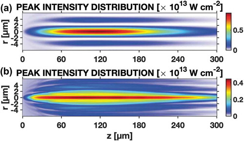
Figure 8. (a) Nanogratings formed in fused silica under ultrafast multipulse Bessel irradiation. (b) Electromagnetic calculus of planes of electronic excitation suggesting the arrangement in nanoplanes under Bessel illumination. Data from Ref [Citation107].
![Figure 8. (a) Nanogratings formed in fused silica under ultrafast multipulse Bessel irradiation. (b) Electromagnetic calculus of planes of electronic excitation suggesting the arrangement in nanoplanes under Bessel illumination. Data from Ref [Citation107].](/cms/asset/c6e5fc93-f22f-4e3f-9e20-0436f39c6ee3/tapx_a_1659180_f0008_oc.jpg)