Figures & data
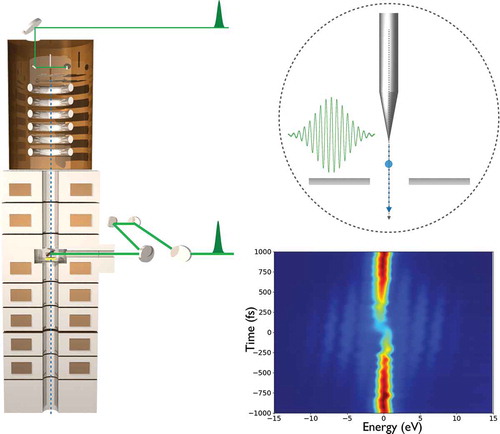
Figure 1. (Color Online) (a) Ultrafast Transmission Electron Microscope based on a laser-driven cold-field emission source. (b) Close-up of the tip region: the [310] oriented tungsten nanotip is placed in front of an extraction anode and illuminated by femtosecond laser pulses (250 fs, 515 nm). (c) Potential of an electron at the metal/vacuum interface. The potential is lowered by the Schottky effect due to the applied extraction voltage . In our experimental conditions, electron emission is triggered by the absorption of two photons (
eV).
![Figure 1. (Color Online) (a) Ultrafast Transmission Electron Microscope based on a laser-driven cold-field emission source. (b) Close-up of the tip region: the [310] oriented tungsten nanotip is placed in front of an extraction anode and illuminated by femtosecond laser pulses (250 fs, 515 nm). (c) Potential of an electron at the metal/vacuum interface. The potential is lowered by the Schottky effect due to the applied extraction voltage VDC. In our experimental conditions, electron emission is triggered by the absorption of two photons (Ephot=2.41 eV).](/cms/asset/82cc4b45-1d1b-42ee-a5c9-9e210aa5e4e0/tapx_a_1660214_f0001_oc.jpg)
Figure 2. (Color Online) (a) A femtosecond laser pulse is incident on a metallic nanotip: the ultrafast dynamics of the excited electron gas involves optical excitation by the laser pulse, electron-electron and electron–phonon interactions on a femtosecond timescale. The laser pulse intensity is maximum on the nanotip at t = 0 fs. b) Left: Electron occupation number as a function of energy at t = 0 fs. Center: electron potential at the metal/vacuum interface. Right: Instantaneous spectral density of emitted current .
eV is the maximum of the potential barrier.
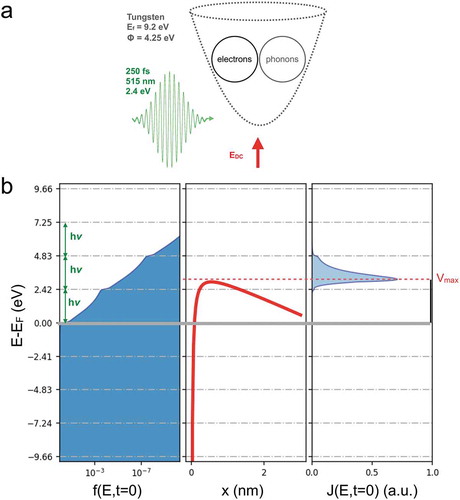
Figure 3. (Color Online) (a) Spectrum of the electron pulse computed in laser-driven mode. Inset: electron energy spectrum computed for a conventional DC cold-field emission source. (b) Temporal profile of the emitted electron pulse. The results in (a) and (b) have been computed for an excess energy density (solid line) and
(dashed line). (c) Number of electrons per pulse per unit surface as a function of the excess energy density. d) Dependence of the temporal (red triangles) and energy (blue dots) width (FWHM) on the excess energy density.
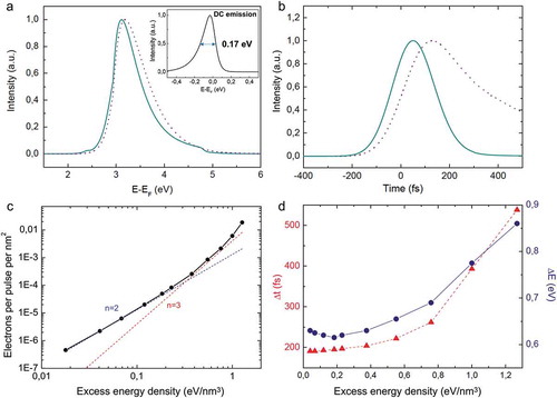
Figure 4. (Color Online) Electron pulse duration (a) and energy spread (b) as a function of propagation time for two different numbers of numbers per pulse. We assume that the electron pulse has an initial radius of 320 , a kinetic energy of 150 kV and an initial duration of 300 fs.
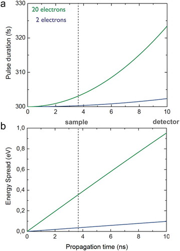
Figure 5. (Color Online) a) Zero-Loss Spectrum of the electron pulse in laser-driven mode for different number of electrons per pulse. Inset: Zero-loss spectrum measured in DC mode. b) FWHM of the electron energy spectrum as a function of the number of electrons per pulse. c) Minimum achievable electron spot size (FWHM) as a function of the number of electrons per pulse.
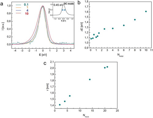
Figure 6. (Color Online) (a) Electron energy spectrum measured in the vicinity of a tungsten nanotip as a function of the delay between the electron pulse and the femtosecond laser pulse. (b) Difference between the spectra measured in a) and the electron spectrum measured without optical excitation. The data have been acquired with electron pulses having eight electrons per pulse in the gun. The optical excitation wavelength was 515 nm (2.41 eV). (c) and (d) Numerical simulations of the results presented in (a) and (b).
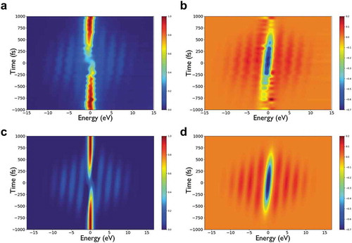
Figure 7. (Color Online) (a) Electron pulse duration determined from systematic EEGS experiments as a function of the number of electrons per pulse emitted in the electron gun. (b) Chirp of the electron pulses as a function of the number of electrons per pulse.
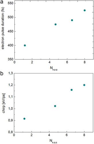
Figure 8. (Color Online) (a) Electron holograms recorded in the vacuum using ultrashort electron pulses as a function of the number of electrons per pulse . (b) Extracted electrons phase and measure of the phase standard deviation. Experimental conditions: 150 keV electrons,
MHz, binning 2, Magnification = 400 kX, Biprism voltage = 30 V, Stack of 90 holograms acquired with 20 s of individual exposure time [Citation62].
![Figure 8. (Color Online) (a) Electron holograms recorded in the vacuum using ultrashort electron pulses as a function of the number of electrons per pulse Nepp. (b) Extracted electrons phase and measure of the phase standard deviation. Experimental conditions: 150 keV electrons, flaser=2 MHz, binning 2, Magnification = 400 kX, Biprism voltage = 30 V, Stack of 90 holograms acquired with 20 s of individual exposure time [Citation62].](/cms/asset/1ea3d479-ba3a-4f99-b62e-fed9b1500c5e/tapx_a_1660214_f0008_oc.jpg)
Figure 9. (Color Online) Two beam (004) CBED patterns and rocking curve profiles acquired on a Silicon lamella with 1) 20 s of exposure time using ultrashort electron pulses, 2) 30 min of exposure time, thanks to a stack of 90 CBED patterns of 20 s of individual exposure time, using ultrashort electron pulses and 3) 0,5 s of exposure time using a continuous electron beam. Experimental conditions of the ultrafast electron source: 150 keV electrons, mW,
,
MHz.
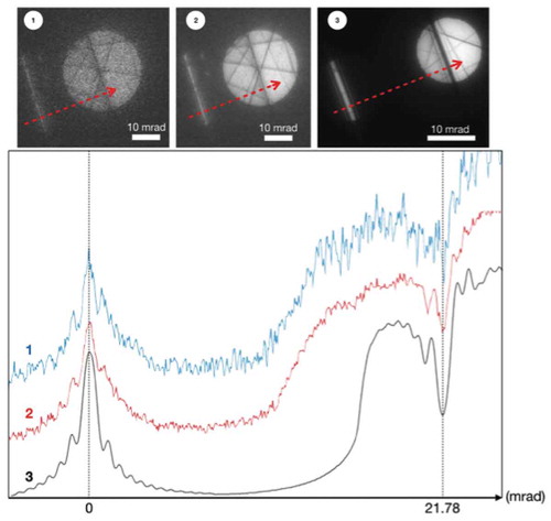
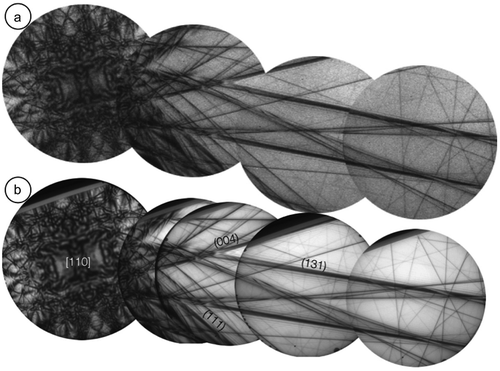
Figure 10. (Color Online) LACBED patterns obtained on a Si lamella under the same conditions using ultrashort electrons pulses and 150 s of exposure time (a) and continuous electron beam and 0,5 s of exposure time (b). Experimental conditions of the ultrafast electron source: 150 keV electrons, mW,
,
MHz.