
Figures & data
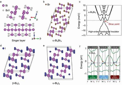
Figure 1. Crystal structure of Bi4X4 (X = Br or I). a, crystal structure of a Bi4X4 1D chain. the gray balls and the pink balls are Br/I and Bi atoms, respectively. b-d, crystal structures of α-Bi4Br4 (b), β-Bi4I4 (c) and α-Bi4I4 (d) viewed from the chain direction (b direction). The brown balls and the blue balls are Br and I atoms, respectively. Figures reproduced from: (a) ref [Citation74], copyright 2014, American Chemical Society; (b,c,d) ref [Citation65] copyright 2021, Nature Publishing Group. β.
![Figure 1. Crystal structure of Bi4X4 (X = Br or I). a, crystal structure of a Bi4X4 1D chain. the gray balls and the pink balls are Br/I and Bi atoms, respectively. b-d, crystal structures of α-Bi4Br4 (b), β-Bi4I4 (c) and α-Bi4I4 (d) viewed from the chain direction (b direction). The brown balls and the blue balls are Br and I atoms, respectively. Figures reproduced from: (a) ref [Citation74], copyright 2014, American Chemical Society; (b,c,d) ref [Citation65] copyright 2021, Nature Publishing Group. β.](/cms/asset/e49fea6f-85ae-4e81-a096-dd90e2d4b2cc/tapx_a_2057234_f0001_oc.jpg)
Figure 2. a, The edge density of states (first row) and spin polarization (second row) for single-layer, double-layer, and triple-layer Bi4Br4. The Fermi level is set to the bulk band gap center. b, At the stair-stepped edge, single-Dirac-cone edge states from the two different layers are degenerate, thus are decoupled in real space. c, Schematic diagram of the band evolution. The explanation is shown in the main text. Schematic figure (right corner) of the single-layer Bi4Br4 structure with Br atoms neglected. The filled and empty circles stand for Bi atoms from adjacent chains. The solid lines denote strong intrachain bonds, the dash lines denote weak interchain coupling. d, e, f, The bulk electronic band structures of α-Bi4Br4 and β-Bi4Br4, where SOC are included and HSE are employed. The symbols + and – label the parity eigenvalues of the band edges at L and M points. The dashed lines indicate Fermi levels. A band gap is opened for α-Bi4Br4 in d, whereas gapless topological hinge states emerge for α-Bi4Br4 in e; the Dirac point is indicated by the red arrow. β-Bi4Br4 is a WTI with (0;001) invariants and a 32 meV indirect gap. The (100) surface states exhibit two anisotropy surface Dirac cones with the absence of dangling bond states. g, h, i, The bulk band structures for α-Bi4I4 and β-Bi4I4 with the SOC. The dashed lines are the Fermi levels. A band gap is opened for α-Bi4I4 in g. β-Bi4I4 is an STI with (1;110) invariants and a 39 meV indirect gap with one highly anisotropic surface Dirac cone at the (001) cleavage surface in h. In i, the red and blue circles label respectively the even parities and odd parities for the bulk bands at the M and L points. The gap size was adjusted by varying the parameters in mBJ. The Z2 invariants cannot be confidently determined from theory alone, given that β-Bi4I4 is in proximity to three different phases, namely an STI (1;110), a WTI (0;001), or even a normal insulator (0;000), all of which are found within a small range of bandgap variation beyond the accuracy of theoretical calculations. Figure reproduced from (a,b) ref [Citation75] copyright 2015, Institute of Physics; (c) ref [Citation74] copyright 2014, American Chemical Society; (d,f,g,h) ref [Citation62] copyright 2014, American Physical Society; (e) ref [Citation65] copyright 2021, Nature Publishing Group; (i) ref [Citation63] copyright 2019, Nature Publishing Group.
![Figure 2. a, The edge density of states (first row) and spin polarization (second row) for single-layer, double-layer, and triple-layer Bi4Br4. The Fermi level is set to the bulk band gap center. b, At the stair-stepped edge, single-Dirac-cone edge states from the two different layers are degenerate, thus are decoupled in real space. c, Schematic diagram of the band evolution. The explanation is shown in the main text. Schematic figure (right corner) of the single-layer Bi4Br4 structure with Br atoms neglected. The filled and empty circles stand for Bi atoms from adjacent chains. The solid lines denote strong intrachain bonds, the dash lines denote weak interchain coupling. d, e, f, The bulk electronic band structures of α-Bi4Br4 and β-Bi4Br4, where SOC are included and HSE are employed. The symbols + and – label the parity eigenvalues of the band edges at L and M points. The dashed lines indicate Fermi levels. A band gap is opened for α-Bi4Br4 in d, whereas gapless topological hinge states emerge for α-Bi4Br4 in e; the Dirac point is indicated by the red arrow. β-Bi4Br4 is a WTI with (0;001) invariants and a 32 meV indirect gap. The (100) surface states exhibit two anisotropy surface Dirac cones with the absence of dangling bond states. g, h, i, The bulk band structures for α-Bi4I4 and β-Bi4I4 with the SOC. The dashed lines are the Fermi levels. A band gap is opened for α-Bi4I4 in g. β-Bi4I4 is an STI with (1;110) invariants and a 39 meV indirect gap with one highly anisotropic surface Dirac cone at the (001) cleavage surface in h. In i, the red and blue circles label respectively the even parities and odd parities for the bulk bands at the M and L points. The gap size was adjusted by varying the parameters in mBJ. The Z2 invariants cannot be confidently determined from theory alone, given that β-Bi4I4 is in proximity to three different phases, namely an STI (1;110), a WTI (0;001), or even a normal insulator (0;000), all of which are found within a small range of bandgap variation beyond the accuracy of theoretical calculations. Figure reproduced from (a,b) ref [Citation75] copyright 2015, Institute of Physics; (c) ref [Citation74] copyright 2014, American Chemical Society; (d,f,g,h) ref [Citation62] copyright 2014, American Physical Society; (e) ref [Citation65] copyright 2021, Nature Publishing Group; (i) ref [Citation63] copyright 2019, Nature Publishing Group.](/cms/asset/16059088-a03d-4653-b13d-4483038d00ec/tapx_a_2057234_f0002_oc.jpg)
Figure 3. Angle-resolved photoemission spectroscopy spectra of β-Bi4I4. a, Constant energy contour map at a binding energy Ebind = 0.040 eV spanning several Brillouin zones, measured at hν = 85 eV. b, Band dispersion covering a large energy and momentum range along the high-symmetry direction (kx = 0.45 Å−1) following the boundary of the first BZ. c, High-resolution close-up of the band dispersion around the
point measured along the y direction. The extracted Fermi velocity is VFy = 0.6(4)×106 m s−1. d, Band dispersion measured along line
(ky = 0 Å−1) crossing the first BZ. For this direction, we obtain a Fermi velocity of VFx = 0.1(1)×106 m s−1. e, Computed weights of the surface and bulk states at the
point as a function of distance to the surface and energy relative to the surface-state Dirac point. This demonstrates strong surface localization of the topological Dirac fermion states (E = 0 in this plot). f, Details of the band dispersion around the
point measured with an ultraviolet laser (hν = 6 eV). g, Energy dispersion curves (EDCs) at
for hν = 6 eV and hν = 68 eV measurements. The arrow points to the shoulder attributed to the bulk VB. Figure reproduced from ref [Citation61] copyright 2016, nature publishing group.
![Figure 3. Angle-resolved photoemission spectroscopy spectra of β-Bi4I4. a, Constant energy contour map at a binding energy Ebind = 0.040 eV spanning several Brillouin zones, measured at hν = 85 eV. b, Band dispersion covering a large energy and momentum range along the high-symmetry direction Γ′‾−Mˉ−Γ′‾ (kx = 0.45 Å−1) following the boundary of the first BZ. c, High-resolution close-up of the band dispersion around the Mˉ point measured along the y direction. The extracted Fermi velocity is VFy = 0.6(4)×106 m s−1. d, Band dispersion measured along line Mˉ−Γˉ−Mˉ (ky = 0 Å−1) crossing the first BZ. For this direction, we obtain a Fermi velocity of VFx = 0.1(1)×106 m s−1. e, Computed weights of the surface and bulk states at the Mˉ point as a function of distance to the surface and energy relative to the surface-state Dirac point. This demonstrates strong surface localization of the topological Dirac fermion states (E = 0 in this plot). f, Details of the band dispersion around the Mˉ point measured with an ultraviolet laser (hν = 6 eV). g, Energy dispersion curves (EDCs) at Mˉ for hν = 6 eV and hν = 68 eV measurements. The arrow points to the shoulder attributed to the bulk VB. Figure reproduced from ref [Citation61] copyright 2016, nature publishing group.](/cms/asset/f0f031f9-6bb3-407b-b0b9-c9cfb410d2ae/tapx_a_2057234_f0003_oc.jpg)
Figure 4. A, ARPES intensity plots for α-Bi4I4, β-Bi4I4 and Bi4Br4 taken along the normal emission with respect to the ab cleavage plane. b, same as a, but the color contrast in the image is changed by a factor of 20 to enhance the visibility of the topological in-gap states. c, momentum distribution curves (MDCs) at E – EF = −0.06 eV, which is about the energy for the dirac point in Bi4Br4. d, The same data as in c, but zoomed in the vertical axis. e, schematics of topological properties of Bi4I4 and Bi4Br4. Figure reproduced from ref [Citation65] copyright 2021, Nature Publishing Group.
![Figure 4. A, ARPES intensity plots for α-Bi4I4, β-Bi4I4 and Bi4Br4 taken along the normal emission with respect to the ab cleavage plane. b, same as a, but the color contrast in the image is changed by a factor of 20 to enhance the visibility of the topological in-gap states. c, momentum distribution curves (MDCs) at E – EF = −0.06 eV, which is about the energy for the dirac point in Bi4Br4. d, The same data as in c, but zoomed in the vertical axis. e, schematics of topological properties of Bi4I4 and Bi4Br4. Figure reproduced from ref [Citation65] copyright 2021, Nature Publishing Group.](/cms/asset/e0f5a582-2fd0-4693-8a20-b80e5cdc0f50/tapx_a_2057234_f0004_oc.jpg)
Figure 5. Topological edge states of Bi4Br4 and Bi4I4 observed by scanning tunneling microscopy. a, Topological edge state residing at the single-layer step edge of the (001) facet of an as-grown α-Bi4Br4 nanowire. (a) STM image of a single-layer step edge on the (001) side surface. Note that this image has been flattened. Vb = −0.5 V, It = 20 pA, T = 5 K. (b) dI/dV spectra collected at the locations (marked by the white and red dots) along the straight line perpendicular to the step edge in (a). (c) dI/dV spectra collected at the locations (marked by the red dots) along the step edge in (a). The topological edge state resides at the hinge between the (102) top surface and the (001) side surface of an as-grown α-Bi4Br4 nanowire. b, (a) Derivative STM image of the hinge between the (102) top surface and the (001) side surface. The derivative image is adopted for a clear illustration of both the (102) top surface and the (001) side surface. Vb = −1 V, It = 50 pA, T = 5 K. (b) dI/dV spectra collected at the locations (marked by the colored dots) along the straight line perpendicular to the hinge in (a). (c-f) dI/dV maps of the same region of (a) taken at various sample biases. c, 1D edge states. (a) Topography of Bi4I4 nanoribbon (Vbias = 0.15 V, I = 300 pA, 15 nm × 25 nm). The blue dashed circles and green dashed circles represent the surface adsorbate and lattice distortion, respectively. (b) dI/dV spectra obtained in the inner terrace (black) and edge (blue) regions of Bi4I4 nanoribbon in (a). The red and purple triangles are presented for the valence band maximum (VBM) and conduction band minimum (CBM), respectively. (c) dI/dV image collected with the bias at 150 mV of Bi4I4 nanoribbon in (a). The white dashed lines are marked for the guidance of dispersion of the 1D edge state. (d) Stacked dI/dV images of the area shown in (a) recorded at voltages across the bandgap as marked on the left. d, dI/dV images (15 nm × 25 nm) were recorded at different voltages. (a-d) inside and (e-h) outside bandgap. The white dashed lines are marked for the guidance of dispersion of the 1D edge state. The identical dispersion of the 1D edge state regardless of the different voltages indicates the robustness of the 1D edge state. Figure reproduced from (a,b) ref [Citation76] Copyright 2021, American Chemical Society; (c,d) ref [Citation78] copyright 2021, American Chemical Society.
![Figure 5. Topological edge states of Bi4Br4 and Bi4I4 observed by scanning tunneling microscopy. a, Topological edge state residing at the single-layer step edge of the (001) facet of an as-grown α-Bi4Br4 nanowire. (a) STM image of a single-layer step edge on the (001) side surface. Note that this image has been flattened. Vb = −0.5 V, It = 20 pA, T = 5 K. (b) dI/dV spectra collected at the locations (marked by the white and red dots) along the straight line perpendicular to the step edge in (a). (c) dI/dV spectra collected at the locations (marked by the red dots) along the step edge in (a). The topological edge state resides at the hinge between the (102) top surface and the (001) side surface of an as-grown α-Bi4Br4 nanowire. b, (a) Derivative STM image of the hinge between the (102) top surface and the (001) side surface. The derivative image is adopted for a clear illustration of both the (102) top surface and the (001) side surface. Vb = −1 V, It = 50 pA, T = 5 K. (b) dI/dV spectra collected at the locations (marked by the colored dots) along the straight line perpendicular to the hinge in (a). (c-f) dI/dV maps of the same region of (a) taken at various sample biases. c, 1D edge states. (a) Topography of Bi4I4 nanoribbon (Vbias = 0.15 V, I = 300 pA, 15 nm × 25 nm). The blue dashed circles and green dashed circles represent the surface adsorbate and lattice distortion, respectively. (b) dI/dV spectra obtained in the inner terrace (black) and edge (blue) regions of Bi4I4 nanoribbon in (a). The red and purple triangles are presented for the valence band maximum (VBM) and conduction band minimum (CBM), respectively. (c) dI/dV image collected with the bias at 150 mV of Bi4I4 nanoribbon in (a). The white dashed lines are marked for the guidance of dispersion of the 1D edge state. (d) Stacked dI/dV images of the area shown in (a) recorded at voltages across the bandgap as marked on the left. d, dI/dV images (15 nm × 25 nm) were recorded at different voltages. (a-d) inside and (e-h) outside bandgap. The white dashed lines are marked for the guidance of dispersion of the 1D edge state. The identical dispersion of the 1D edge state regardless of the different voltages indicates the robustness of the 1D edge state. Figure reproduced from (a,b) ref [Citation76] Copyright 2021, American Chemical Society; (c,d) ref [Citation78] copyright 2021, American Chemical Society.](/cms/asset/1ba101aa-60ee-4efc-8dc9-00ab91a18152/tapx_a_2057234_f0005_oc.jpg)
Figure 6. Quantum transport properties of the bulk α-Bi4I4 and β-Bi4I4. a, α-Bi4I4 (a) The resistance derivative /
versus 1/
=
in sample A1 (N-type) at varied tilt angles
(T = 2 K). The inset depicts the measurement configuration, where
is defined as the angle between the direction of the magnetic field and normal direction of the sample substrate (//ab plane). The dashed lines in the main panel mark the positions of maxima. (b) The resistance derivative
/
versus B in sample B2 (P-type) at selected tilt angles
from 0° to 120° (T = 2 K). The quantum oscillations survive at all measured tilt angles
. (c) and (d) show the field positions of the oscillating extremums for sample A1 and B2 respectively. The dashed lines are
/
fit for sample A1 and tentative
/
curves for B2. (e) The
curves as a function of
at 2 K and at lower field for sample A1. b, β-Bi4I4 (a) The field dependence of ρxx up to 43 T under different temperatures. The red dashed line marks the ending of the quantum oscillation, above which the system enters the EQL. The inset shows the metal to insulator transition happens at a critical field of 15.9 T. (b) Plot of the ρxx as a function of temperature at fixed magnetic field B. (c) The field dependence of ρxy up to 43 T. (d) Scaling plot of the normalized ρxx; all the isotherms fall onto a nearly single curve as a function of |B − Bc|T−1/ζ with ζ ≈ 6.5; the inset shows the linear fitting of the log(dρxx/dB) at Bc vs log(1/T), which yields 1/ζ. Figure reproduced from (a) ref [Citation82] copyright 2018, American Physical Society; (c,d) ref [Citation83] copyright 2021, American Physical Society.
![Figure 6. Quantum transport properties of the bulk α-Bi4I4 and β-Bi4I4. a, α-Bi4I4 (a) The resistance derivative dRxx/dB versus 1/Bv = 1/Bcosθ in sample A1 (N-type) at varied tilt angles θ (T = 2 K). The inset depicts the measurement configuration, where θ is defined as the angle between the direction of the magnetic field and normal direction of the sample substrate (//ab plane). The dashed lines in the main panel mark the positions of maxima. (b) The resistance derivative dRxx/dB versus B in sample B2 (P-type) at selected tilt angles θ from 0° to 120° (T = 2 K). The quantum oscillations survive at all measured tilt angles θ. (c) and (d) show the field positions of the oscillating extremums for sample A1 and B2 respectively. The dashed lines are B0/cosθ fit for sample A1 and tentative B0/cosθ−30∘ curves for B2. (e) The ρxx curves as a function of Bv at 2 K and at lower field for sample A1. b, β-Bi4I4 (a) The field dependence of ρxx up to 43 T under different temperatures. The red dashed line marks the ending of the quantum oscillation, above which the system enters the EQL. The inset shows the metal to insulator transition happens at a critical field of 15.9 T. (b) Plot of the ρxx as a function of temperature at fixed magnetic field B. (c) The field dependence of ρxy up to 43 T. (d) Scaling plot of the normalized ρxx; all the isotherms fall onto a nearly single curve as a function of |B − Bc|T−1/ζ with ζ ≈ 6.5; the inset shows the linear fitting of the log(dρxx/dB) at Bc vs log(1/T), which yields 1/ζ. Figure reproduced from (a) ref [Citation82] copyright 2018, American Physical Society; (c,d) ref [Citation83] copyright 2021, American Physical Society.](/cms/asset/515fc642-cad2-4269-b744-5a204efd1912/tapx_a_2057234_f0006_oc.jpg)
Figure 7. (a) Temperature dependence of resistance at various pressures P 3.8 GPa. (b), Temperature dependence of resistance around Tc. (c), temperature dependence of AC magnetic susceptibility up to 10.0 GPa. (d), determination of the upper critical field μ0Hc(0). (e), T-P phase diagram of α-Bi4Br4. (f), magnetic field dependence of resistance of α-Bi4Br4 crystal at different pressures. Figure reproduced from ref [Citation69] copyright 2019 National Academy of Sciences.
![Figure 7. (a) Temperature dependence of resistance at various pressures P ≥ 3.8 GPa. (b), Temperature dependence of resistance around Tc. (c), temperature dependence of AC magnetic susceptibility up to 10.0 GPa. (d), determination of the upper critical field μ0Hc(0). (e), T-P phase diagram of α-Bi4Br4. (f), magnetic field dependence of resistance of α-Bi4Br4 crystal at different pressures. Figure reproduced from ref [Citation69] copyright 2019 National Academy of Sciences.](/cms/asset/3e6224e6-5910-4be1-b305-e8da11dcc9d4/tapx_a_2057234_f0007_oc.jpg)
Figure 8. Evolution of the electrical resistivity as a function of pressure and the electronic P-T phase diagram for α-Bi4I4. a, b, Electrical resistivity as a function of temperature for pressures up to 40 GPa. The temperature dependence of ρ(T) changes from semiconducting-like behavior to that of a normal metal. c, d, Electrical resistivity drop and zero-resistivity behavior at low temperature for pressures of 13.5–23.0 and 24.1–39.5 GPa, respectively. Here, Tc increases under increasing pressure and the maximum superconducting transition temperature corresponds to Tc = 6 K at 23.0 GPa. e, Temperature dependence of resistivity under different magnetic fields for α-Bi4I4 at 21.8 GPa. f, Temperature dependence of the upper critical field for α-Bi4I4. Here, Tc is determined as the 90% drop of the normal state resistivity. The solid lines represent the fits based on the Ginzburg-Landau formula. g, Superconducting Tc is shown as a function of pressure. The green and blue circles represent the Tc extracted from different resistivity measurements. As the pressure increases to 13 GPa, superconductivity is observed above experimental Tmin and persists up to pressures near 40 GPa. A dome-like evolution is observed with a maximum Tc of 6 K attained at P = 23 GPa. The resistivity values at 300 K are also shown. The resistivity of α-Bi4I4 exhibits a more complicated feature, which demonstrates that high pressure dramatically alters the electronic properties in α-Bi4I4. h, Schematic illustrations of the band structure evolution under various pressures. In the STI phase, band inversion occurs at one time-reversal-invariant momentum (TRIM) point of the Brillouin zone; however, in the WTI phase, band inversion occurs at two TRIM points. Figure reproduced from ref [Citation71] copyright 2018, Nature Publishing Group.
![Figure 8. Evolution of the electrical resistivity as a function of pressure and the electronic P-T phase diagram for α-Bi4I4. a, b, Electrical resistivity as a function of temperature for pressures up to 40 GPa. The temperature dependence of ρ(T) changes from semiconducting-like behavior to that of a normal metal. c, d, Electrical resistivity drop and zero-resistivity behavior at low temperature for pressures of 13.5–23.0 and 24.1–39.5 GPa, respectively. Here, Tc increases under increasing pressure and the maximum superconducting transition temperature corresponds to Tc = 6 K at 23.0 GPa. e, Temperature dependence of resistivity under different magnetic fields for α-Bi4I4 at 21.8 GPa. f, Temperature dependence of the upper critical field for α-Bi4I4. Here, Tc is determined as the 90% drop of the normal state resistivity. The solid lines represent the fits based on the Ginzburg-Landau formula. g, Superconducting Tc is shown as a function of pressure. The green and blue circles represent the Tc extracted from different resistivity measurements. As the pressure increases to ≈ 13 GPa, superconductivity is observed above experimental Tmin and persists up to pressures near 40 GPa. A dome-like evolution is observed with a maximum Tc of 6 K attained at P = 23 GPa. The resistivity values at 300 K are also shown. The resistivity of α-Bi4I4 exhibits a more complicated feature, which demonstrates that high pressure dramatically alters the electronic properties in α-Bi4I4. h, Schematic illustrations of the band structure evolution under various pressures. In the STI phase, band inversion occurs at one time-reversal-invariant momentum (TRIM) point of the Brillouin zone; however, in the WTI phase, band inversion occurs at two TRIM points. Figure reproduced from ref [Citation71] copyright 2018, Nature Publishing Group.](/cms/asset/7ee49f43-8db2-41d9-b753-6cc3eeb0df0e/tapx_a_2057234_f0008_oc.jpg)