
Figures & data
Figure 1. (a) Schematic of the room temperature bonding process of diamond and InGaP. (b,c) AFM images of the diamond and the InGaP surface, respectively. (c) Optical microscope image of the diamond/InGaP bonded sample surface.
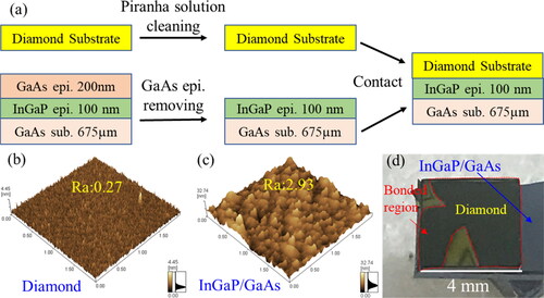
Figure 2. (a) C1s and (b) O1s spectra of diamond, (c) In3d, (d) Ga2p, (e) P2p, and (f) O1s spectra of InGaP.
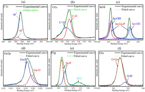
Figure 3. (a) Low-magnification cross-sectional TEM image, (b) HRTEM image taken along the InGaP [001] direction, (c) HRTEM image taken along the diamond [001] direction, (d) EDS mappings, and (e) X-ray intensity profiles of C, P, In, Ga, and O elements of the bonding interface before annealing.
![Figure 3. (a) Low-magnification cross-sectional TEM image, (b) HRTEM image taken along the InGaP [001] direction, (c) HRTEM image taken along the diamond [001] direction, (d) EDS mappings, and (e) X-ray intensity profiles of C, P, In, Ga, and O elements of the bonding interface before annealing.](/cms/asset/60a4185a-9bbe-432e-9ff6-0c2ca1d9a8f4/tfdi_a_1869435_f0003_c.jpg)
Figure 4. (a) Low-magnification cross-sectional TEM image, (b) HRTEM image taken along the InGaP [001] direction, (c) HRTEM image taken along the diamond [001] direction, (d) EDS mappings, and (e) X-ray intensity profiles of C, P, In, Ga, and O elements of the bonding interface after annealing at 400 °C.
![Figure 4. (a) Low-magnification cross-sectional TEM image, (b) HRTEM image taken along the InGaP [001] direction, (c) HRTEM image taken along the diamond [001] direction, (d) EDS mappings, and (e) X-ray intensity profiles of C, P, In, Ga, and O elements of the bonding interface after annealing at 400 °C.](/cms/asset/e3e0326c-2cf0-4d9e-bb30-71644c941fec/tfdi_a_1869435_f0004_c.jpg)