Figures & data
Table 1. Summarization of HPHT technology for large crystal producing.
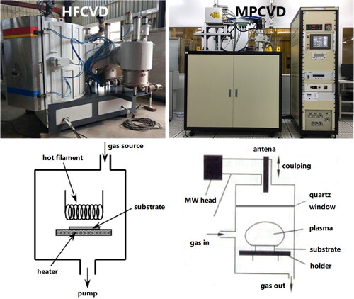
Table 2. Comparison of different CVD techniques.
Table 3. Summarization of large area diamond film.

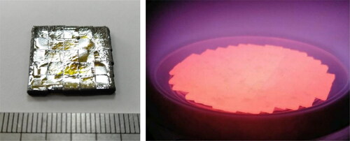
![Figure 3. More than 10 ct white and yellow HPHT diamond jewelry by NDT company [Citation17].](/cms/asset/02319c56-b7a1-4522-98cf-63bb1b7c9373/tfdi_a_1869511_f0003_c.jpg)
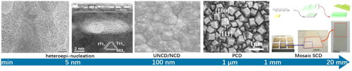
![Figure 6. Schematic of diamond “mosaic” growth process [Citation34].](/cms/asset/8f47c3f3-75a3-4e0c-a388-2698cf204630/tfdi_a_1869511_f0006_c.jpg)
![Figure 7. Schematics of “Lift-off” technology for clone substrates production (top picture), and the 1–2 inch mosaic samples (bottom images) [Citation49–51].](/cms/asset/468dd0cb-63c3-418c-ae7d-0f76d912a842/tfdi_a_1869511_f0007_c.jpg)
![Figure 9. Epitaxial lateral overgrowth (ELO) of CVD diamond [Citation63, Citation64].](/cms/asset/4c7ea2df-0b76-4d6e-890e-4de42b5ac3fa/tfdi_a_1869511_f0009_c.jpg)
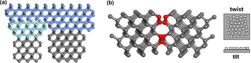
![Figure 10. ELO of SCD by hollowing out the central part of substrate and thus suppress the extension of dislocation [Citation65].](/cms/asset/41ce4cf0-f968-4104-b4c9-d92cd68b1e3a/tfdi_a_1869511_f0010_c.jpg)
![Figure 11. Largest single crystal CVD diamond by heteroepitaxial growth [Citation73].](/cms/asset/3800d91e-dddc-4c6b-8a64-4752aba688b3/tfdi_a_1869511_f0011_c.jpg)
![Figure 12. Evolution of Patterned nucleation growth based on diamond heteroepitaxy [Citation80].](/cms/asset/b3ec9c88-135b-4de8-bfaf-ade44cfe88a1/tfdi_a_1869511_f0012_b.jpg)
![Figure 13. Diamond mosaic detector by CERN [Citation81].](/cms/asset/c52f6209-0aa8-4054-acd3-00e0c1cd5edf/tfdi_a_1869511_f0013_c.jpg)
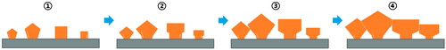
![Figure 15. SEM and schematic of polycrystalline diamond cross-section [Citation86].](/cms/asset/be0f5840-0270-4cba-af8a-5ba8bce301d6/tfdi_a_1869511_f0015_b.jpg)