Figures & data
Table 1. Material properties of copper and molybdenum.
Figure 1. Schemetic representation of pre-growth treatment on (100) oriented CVD grown SCDs.
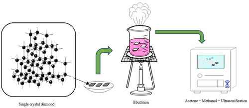
Figure 2. Schematic representation of the arrangement of seed substrates on Molybdenum substrate holder.
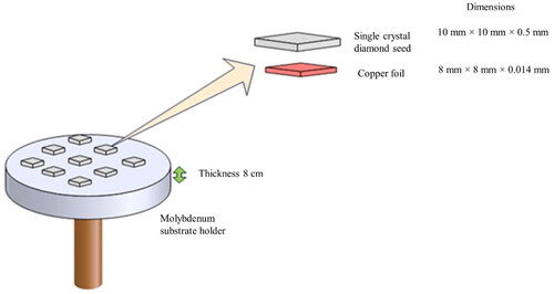
Figure 3. Arrangement of copper foils over Molybdenum holder.
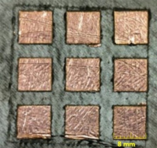
Figure 4. Schematic representation of growth mechanism and creation of species in plasma.
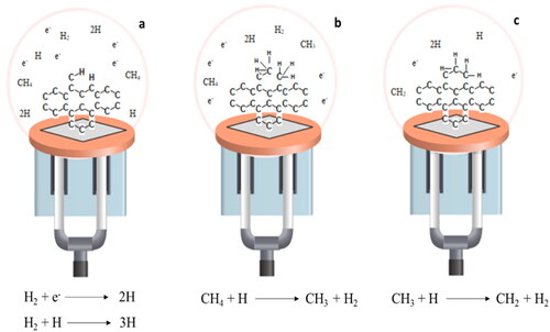
Figure 5. Schematic representation of post growth treatment for grown SCDs.
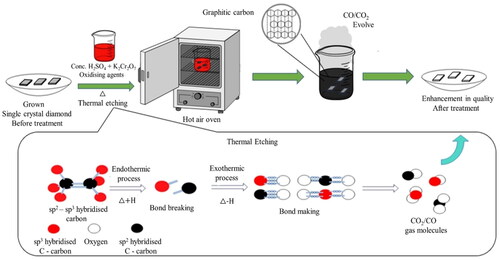
Figure 6. Reported growth of single crystal diamond seeds after (a) 130 h (b) 9 mm× 9 mm × 1.85 mm cubes grown in 171 h process cycle using welding method.
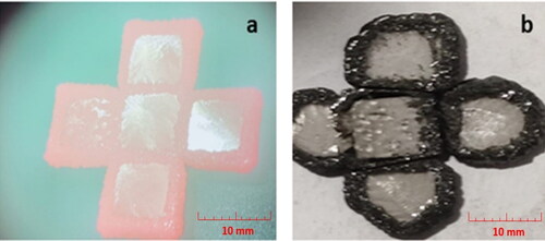
Table 2. Summary of growth parameters.
Figure 7. Reported growths of single crystal diamond seeds after (a) 18 h (b) 25 h (c) 130 h using (d) 9 mm× 9 mm × 1.85 mm cubes grown in 154 h process cycle using welding method.
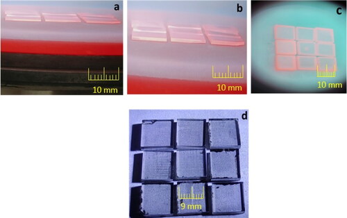
Table 3. Temperature distribution of conventional method for different process cycle.
Table 4. Temperature distribution of welding method for different process cycle.
Figure 8. Comparison between substrate temperatures for different growth cycles for both methods.
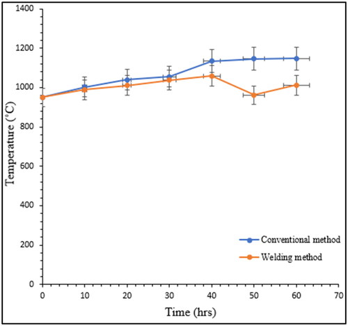
Figure 9. Raman Spectra taken from the samples; Excitation laser wavelength is 532 nm (a) for S1 sample grown using the conventional method (b) for S2 grown using welding method.
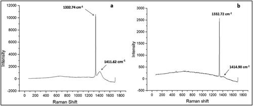
Figure 10. (a) The transmittance spectrum shows maximum transmission at 1336 nm of S1 and (b) Absorbance spectrum shows peak at 220 nm of sample S1.
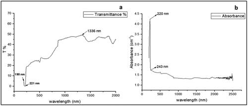
Figure 11. (a) Transmittance spectrum shows maximum transmission at 412 nm of S2 and (b) Absorbance spectrum shows a peak at 282 nm of sample S2.
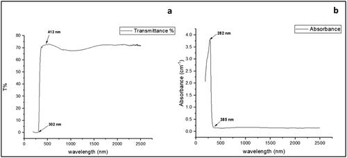
Figure 12. (a) Absorption coefficient spectra shows a peak at 220 nm (b) Absorption coefficient spectra shows zero phonon line at 502 nm of sample S1.
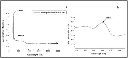
Figure 13. (a) Absorption coefficient spectra shows a peak at 280 nm (b) Absorption coefficient spectra shows zero phonon line at 502 nm of sample S2.
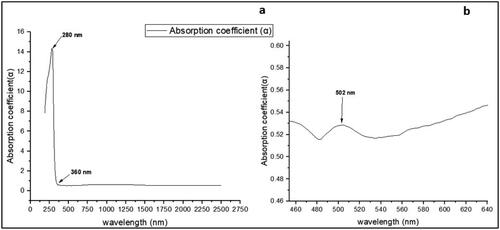
Figure 14. (a) FT-IR spectra of sample S1 over the spectral range 500 cm−1–4000 cm−1 with a peak at 2351.13 cm−1 in two phonon region.
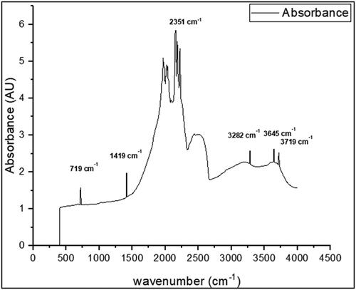
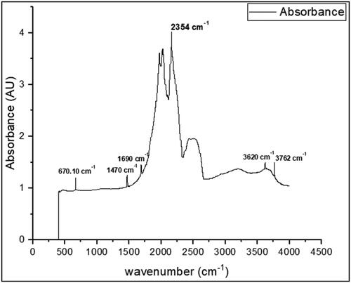
Figure 15. (a) FT-IR spectra of sample S2 over the spectral range 500 cm−1–4000 cm−1 with a peak at 2354.13 cm−1 in two phonon region.