Figures & data
Figure 1 (a) A typical optical image of the plasma flame taken by a digital camera during Si film deposition, (b) a spatial distribution of the normalized intensity of the brightness of the plasma flame at the dashed line position, and (c) a spatial distribution of the normalized intensities of ArI and HI emissions after the Abel inversion analyzed from the OES results.
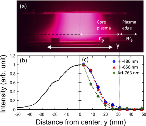
Figure 2 Variation of the deposition rate of the films with the scanning half period at different scan rates deposited on 20 mm × 20 mm substrates. Inset: illustrative diagram for the scanning half period, v: scan rate.
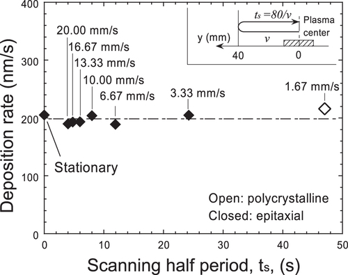
Figure 3 XRD patterns of the films deposited at different scan rates, measured at a 5 mm × 5 mm area of the center of the 20 mm × 20 mm substrates.
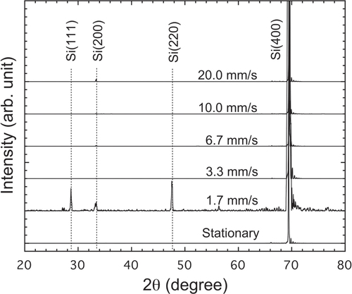
Figure 4 Scan rate dependences of the (a) carrier concentration, (b) resistivity, and (c) Hall mobility of the epitaxial Si films at the center of the samples (20 mm × 20 mm substrate).
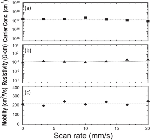
Figure 5 Images of the samples deposited at different scan rates (half parts of the symmetrical samples on 20 mm × 80 mm substrates).
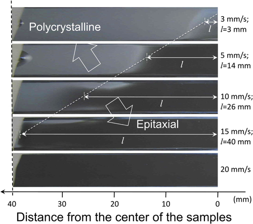
Figure 6 Typical surface (a), (b) and cross-sectional (a′), (b′) SEM images of the films at the white (a), (a′) and black (b), (b′) color regions shown in figure .
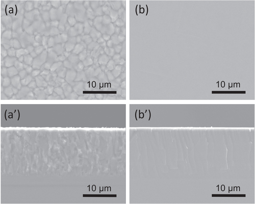
Figure 7 Position dependences of the (a) Hall mobility, (b) surface roughness (rms), and (c) ratio of the plasma core/edge exposure time [τ p/τ e] normalized to their maximum value for the epitaxial Si film deposited at a scan rate of 20 mm s−1.

Figure 8 Measured temperature profile of the substrate at center of the substrate after the plasma turned off and its fitted curve with a lumped capacitance model.
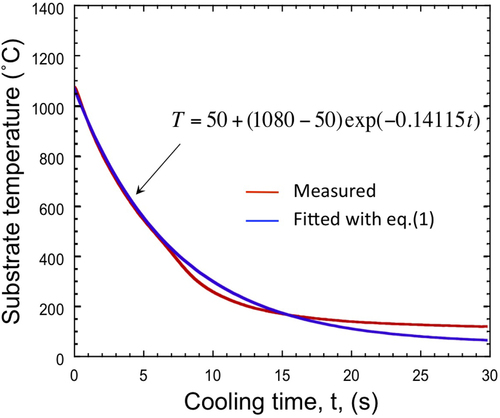
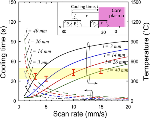
Figure 9 Estimated scan rate dependences of the cooling time and minimum temperature for the substrate at the structure transition region shown in figure . Inset: illustrative diagram of the cooling procedure of the substrate at the structure transition region. (P: polycrystalline; E: epitaxial; υ: scan speed. Dotted line: center of the sample).