
 ?Mathematical formulae have been encoded as MathML and are displayed in this HTML version using MathJax in order to improve their display. Uncheck the box to turn MathJax off. This feature requires Javascript. Click on a formula to zoom.
Abstract
The III-nitride family of semiconductors has proved essential in the design of important optoelectronic technology such as light-emitting diodes (LEDs). To improve our understanding of these materials and their devices it is important to unravel the mysteries of their carrier dynamics. Time-resolved cathodoluminescence (TRCL) is a characterisation technique wherein a pulsed electron beam is used to excite charge carriers in semiconductors. By analysis of the recorded datasets, deductions can be made about the activity of carriers in the period between their generation and recombination. The purpose of this review is to summarise work done on the use of TRCL in the understanding of III-nitride based materials and devices. The focus will be on quantum well LEDs and structural defect-related recombination.
Introduction
The aluminium–indium–gallium nitride (AlInGaN) alloy system of semiconductors has been pivotal in the development of technologically important optoelectronic and electronic devices. From the optoelectronic point-of-view, indium gallium nitride (InGaN) [an alloy of gallium nitride (GaN) and indium nitride (InN)] has paved the way for high-efficiency and high-brightness blue and white light-emitting-diodes (LEDs) for ambient lighting [Citation1–3]. Moreover, InGaN has also proven to be applicable in the green and yellow light emission regimes [Citation4, Citation5]. The implementation of InGaN-based white LEDs for ambient lighting has spurred the move away from traditional light sources such as incandescent and fluorescent light bulbs. Compared to these traditional light sources, LEDs provide improved energy efficiencies, reduced device footprints, longer device lifetimes, and are easily scalable [Citation6–11]. Importantly, by replacing traditional lighting sources, the power-saving nature of InGaN-based white LEDs can not only reduce global carbon emissions, helping to fight climate change, but can also allow people in remote areas access to ambient lighting [Citation12, Citation13]. Apart from LEDs, InGaN has also been crucial in the advancement of other optoelectronic technology including laser diodes (LDs), photovoltaics and photodetectors [Citation14–16].
The light emission range for InGaN lies in between near ultraviolet (UV) ( nm) and near infra infra-red (IR) (
nm) as bound by the band-gap energies (
) of its components which are
eV for GaN and
eV for InGaN [Citation17–19]. To cover light emission in the UV up-to ∼200 nm, aluminium gallium nitride (AlGaN) [an alloy of aluminium nitride (AlN) and GaN] is utilised. AlGaN has been crucial in the design of UV-LEDs for the purposes of water and air purification together with surface sterilisation [Citation20–22]. Being LEDs, these devices offer the same advantages as mentioned above. In addition, their emission wavelength can be tailored by altering the alloy composition allowing for the targeted destruction of a wide range of viruses and bacteria. These advantages make AlGaN-based UV-LEDs more attractive than conventional mercury lamp-based disinfectant systems which are bulky, fragile, emit at a fixed wavelength, and contain hazardous mercury [Citation21, Citation22].
AlInGaN is thus an important materials system that merits extensive research into its properties to aid in the development of superior optoelectronic devices. One such phenomenon crucial in the understanding of semiconducting materials and devices such as LEDs are the charge carrier dynamics. The term ‘charge carriers’ is used to define electrons and holes. These are particles, or pseudoparticles for the case of holes, that carry charge throughout a semiconductor. Hence ‘charge carrier dynamics’ describes the motion and activity of excess electrons and holes in a semiconductor from the point they are generated to when they recombine. An in-depth appreciation of the charge carrier dynamics in semiconductors is key to unravelling a multitude of phenomena such as the density, type and behaviour of structural imperfections (defects), the presence and magnitude of inherent polarisation fields and how they relate to the crystal structure, charge carrier transport, and recombination channels [Citation23–27].
To investigate the carrier dynamics of semiconducting materials, optical excitation based techniques such as scanning near-field optical microscopy (SNOM) and time-resolved photoluminescence (TRPL) can be utilised [Citation28–31]. Some of these techniques, such as SNOM, can overcome the diffraction limit and achieve a nanometre spatial resolution allowing the spatial variation of carrier dynamics to be studied [Citation29]. However, the optical nature of their excitation mechanisms limits their applicability with regard to wide band-gap semiconductors such as GaN ( eV) and AlN (
eV). For instance, SNOM suffers from significant signal loss when UV optics are utilised, while extreme laser powers are required to excite carriers when using TRPL [Citation32]. Time-resolved cathodoluminesce (TRCL) on the other hand employs a focused and pulsed electron beam to study the carrier dynamics in light emitting materials. The high energy electron beam can easily achieve a sub 10 nm beam spot size impinging on the sample surface aiding in the nanometre spatial mapping capabilities of the technique [Citation33]. Importantly, the electron beam energies used are in the keV regime which permits the easy excitation of wide band-gap semiconductors [Citation34].
The purpose of this review is to discuss the application of TRCL to the understanding of AlInGaN-based materials and devices through the interpretation of their carrier dynamics.
Introduction to III-nitride semiconductors
Structural properties
The AlInGaN system, often referred to as the III-nitrides, comprises of group III semiconductors, namely; Ga, In or Al that are bonded to N. For application into optoelectronics such as LEDs, the important crystalline phases of this system to introduce are wurtzite (wz) and zincblende (zb) [Citation35]. Wurtzite is the thermodynamically stable phase at ambient temperature and is the incumbent technology for optoelectronics. As such, the focus of this review will be on wz-based III-nitride materials and optoelectronic devices. Even so, it is important to highlight the metastable zb phase which has received some research interest as a candidate for green and yellow LED applications [Citation36]. The unit cell of the wz phase is shown in Figure along with some important crystal directions and planes.
Figure 1. The crystal structure of wz III-nitrides along with some important crystal planes and directions. The group III species is coloured orange while N is coloured blue.
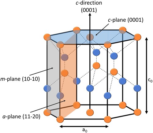
An important feature of the wz unit cell is that it is non-centrosymmetric. In addition to this, the crystal also possesses a unique direction due to a deviation from ideal tetrahedral coordination along the [0001] direction and is thus also polar. These two phenomena result in piezoelectric and spontaneous polarisation fields that act along the [0001] crystal direction or the c-axis [Citation37].
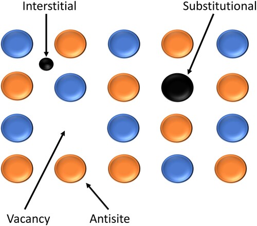
Similar to other materials, the properties of the AlInGaN system will be influenced by the presence of structural defects [Citation38]. Defects interrupt the perfect atomic ordering in a crystal lattice and can appear as intrinsic features at thermodynamic equilibrium. However, external perturbations such as doping, impurities and other conditions involved with their preparation can also influence their formation. For the purposes of this review, the important defects to introduce are point defects, dislocations and stacking faults.
Point defects occur at or around a single point in a crystal and thus have zero dimensionality. Examples of point defects that can exist in III-nitrides are vacancies, interstitials, substitutionals, and antisites as shown in Figure .
Figure 2. Point defects that can exist in III-nitride semiconductors; vacancy, substitutional, interstitial and antisite. The blue and orange spheres represent atoms of the host lattice while black circles illustrate foreign atoms.
Dislocations are one-dimensional disruptions of the crystal ordering. Since III-nitride semiconductor thin films are commonly prepared by growing on substrates which do not match their lattice and thermal expansion coefficient, residual tensile or compressive strain will build up near this interface [Citation39, Citation40]. Dislocations can form in the film to relax some of this strain [Citation41]. Dislocations that lie at the interface to relieve misfit strain are known as misfit dislocations. Those that originate at the ends of the misfit dislocation and thread towards the surface or form a loop are threading dislocations.
Stacking faults are two-dimensional defects which exist because of a partial displacement that affects the regular lattice stacking sequence. In wz III-nitrides, stacking faults that lie along the basal (0001) planes are basal stacking faults while those that lie along the prismatic planes such as (11–20) are prismatic stacking faults.
Device fabrication
To fabricate devices such as LEDs, thin film growth techniques are required. The common growth technique utilised to manufacture III-nitride based thin films and devices is metalorganic vapour phase epitaxy (MOVPE) [Citation42]. Even though this review will focus on III-nitride films prepared using MOVPE, other growth techniques such as molecular beam epitaxy and hydride vapour phase epitaxy can be employed.
Optical properties of semiconductors and carrier diffusion
Radiative and non-radiative recombination
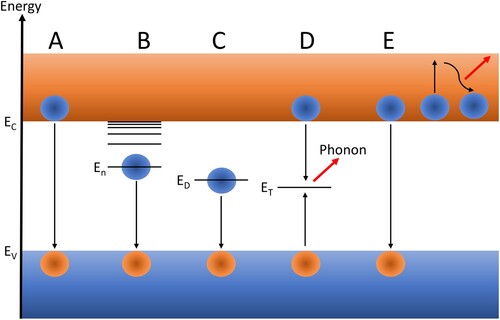
For a semiconductor that is excited by an external perturbation (such as current injection, exposure to light, or electron irradiation) excess electrons and holes are generated. These excess electrons and holes will occupy states in the conduction and valence bands respectively. To restore the system to thermal equilibrium, recombination of excess holes with excess electrons will occur. Recombination processes that lead to the emission of a photon are known as radiative recombination. However, recombination can also take place by a competing process termed non-radiative recombination. During non-radiative recombination no light is emitted; instead, the recombination energy is released as quantised lattice vibrations (phonons) or as hot carriers.
Radiative recombination can be classed as intrinsic or extrinsic. Intrinsic emission occurs due to recombination of a free electron at the edge of the conduction band with a free hole at the edge of the valence band emitting a photon of energy equal to the band gap (E) [Citation43]. This is known as band-edge recombination. Alternatively, a generated electron and hole can lower their energy by forming a bound electron-hole pair known as an exciton [Citation44]. For GaN, the excitonic binding energy is found to be
meV for the A and B excitons at room temperature [Citation45]. Excitonic recombination produces photons of energy just below E
. Extrinsic emission occurs through localised donor or acceptor trap states that exist within the band gap. These states can be provided by defects and foreign atoms such as those from dopants or impurities [Citation46–48]. Examples of extrinsic and intrinsic radiative recombination processes are shown in Figure (a–c). Non-radiative recombination can be divided into two main mechanisms: Shockley-Read-Hall (SRH) [Citation49] and Auger recombination [Citation50]. Similar to extrinsic emission, SRH recombination arises because of the presence of defects such as surfaces, dislocations and point defects. These introduce localised trap states within the band gap [Citation51, Citation52]. An electron can be trapped at a localised defect state and recombine with a hole in the valence band releasing a phonon. Conversely, SRH recombination can also occur through the recombination of a trapped hole with an electron in the conduction band. Auger recombination is a three carrier process. Here, the electron–hole recombination energy is transferred to an electron in the conduction band which thermalises back to the band edges emitting multiple phonons in the process [Citation53]. If the carrier has sufficient energy, it can be emitted from the lattice as a hot carrier. Examples of non-radiative recombination processes are shown in Figure (d) and (e).
Figure 3. Radiative and non-radiative recombination processes in a semiconductor with conduction band-edge energy (E) and valence band-edge energy (E
). (A) describes the band-edge recombination of an electron (blue) and hole (orange). (B) shows excitonic recombination with exciton energy states (E
). (C) is defect assisted radiative recombination with an electron trapped at a donor state of energy (E
). (D) describes SRH recombination at a trap state of energy (E
) and (E) shows the Auger recombination process.
Carrier diffusion
Recombination in an excited semiconductor can be preceded by the motion of carriers from the point of generation to that of recombination. For the case of localised excitation, such is the case with cathodoluminescence, at the point of carrier generation there will be a high concentration of excess carriers producing a concentration gradient. Excess carriers will move from the regions of high concentration to those of low concentration by diffusion until the carrier concentration is uniform. This diffusion process can be characterised by the parameters carrier lifetime (τ) and carrier diffusion length (L) which are related through the diffusion coefficient D by Equation (Equation2(2)
(2) ).
(1)
(1)
Carrier lifetime is the average time that an excess carrier exists between generation and recombination while carrier diffusion length defines the root mean squared displacement of an excess carrier between generation and recombination. Importantly, because of the competitive nature of radiative and non-radiative recombination processes, the effective carrier lifetime () depends on the radiative (
), Auger (
) and SRH (
) carrier lifetimes as shown by Equation (Equation2
(2)
(2) ).
(2)
(2)
Cathodoluminescence and time-resolved cathodoluminescence
Cathodoluminescence microscopy
Cathodoluminescence (CL) is a term used to describe the emission of light from a material, usually a semiconductor, as a result of electron beam irradiation [Citation53]. During this process, primary electrons of energy E interact with the specimen and undergo inelastic scattering processes generating excess electrons and holes with a number in the order of [Citation53]. The excess electrons and holes then recombine to emit photons of light that are collected and used for imaging and spectroscopy in a combined scanning electron microscope cathodoluminescence (SEM-CL) or transmission electron microscope cathodoluminescence (TEM-CL) system [Citation54].
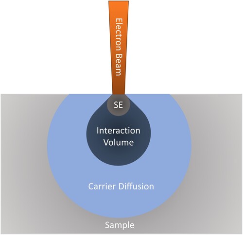
As already mentioned, the use of an electron beam permits the technique to achieve a sub 10-nm beam spot size impinging on the sample surface [Citation33]. This aids in the nanometre scale spatial mapping capabilities of the technique. However, the resolution of CL will mainly depend on the interaction volume and diffusion of excess charge carriers away from the interaction volume. The interaction volume is a region inside the semiconductor within which energy from the electron beam is deposited by inelastic scattering interactions between the primary electrons and the specimen. The size of the interaction volume depends on the penetration depth of primary electrons and increases with the energy of the electron beam. The size of the interaction volume can be numerically approximated by Monte-Carlo simulations [Citation55] or estimated using the Kanaya–Okayama range [Citation56]. The interaction volume can be tuned by controlling the beam energy. However, the carrier diffusion length will control the ultimate spatial resolution that can be achieved. This is rather problematic since the carrier diffusion length is not a material constant and can change based on factors such as; defect density, doping level, and even charge carrier concentration [Citation57, Citation58]. Because of this, defining a spatial resolution for CL is difficult although nanometre spatial mapping is possible. It should be noted that the effects of carrier diffusion can be limited by confinement structures and carrier localisation especially at low temperatures [Citation59, Citation60]. The relationship between the SE generation volume, interaction volume and carrier diffusion is shown in Figure .
Figure 4. Zones within a material where the secondary electrons (SE) are emitted, interaction volume is located, and carrier diffusion occurs. The sizes of the respective zones are not to scale but instead represent the increasing volume of material covered by each successive zone.
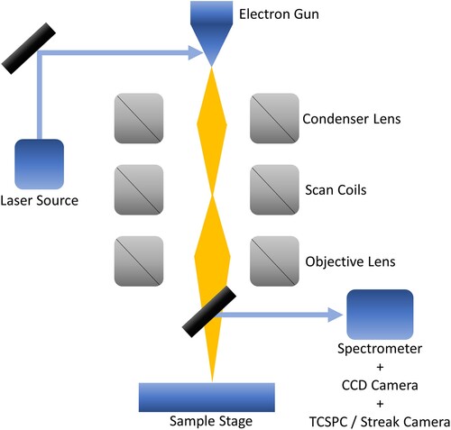
The SEM-CL setup consists of five essential components as shown in Figure . An electron gun that operates by Schottky field emission produces and accelerates primary electrons towards the specimen. Electromagnetic lenses then form a convergent electron beam and focus it on the sample surface. Light emitted from the sample is collected by an optical collection system such as a parabolic mirror and optical fibre that transfers the light to a spectrometer. The spectrometer separates the collected light into its component wavelengths. Finally, the light is recorded by a detector such as a charge-coupled device (CCD) camera.
Figure 5. .The main components of an SEM-CL system.
The main measurement mode worth discussing in CL microscopy is hyperspectral mapping. Here, the electron beam is scanned across the sample surface and a spectrum of the light emitted is collected at each position. The dataset produced thus contains intensity, spatial, and spectral information. The hyperspectral dataset can be sliced to construct panchromatic CL images which show the integrated intensity variation with no spectral selectivity being applied. Monochromatic CL imaging extends panchromatic CL by passing the collected light through a monochromator or band-pass filter. This produces an image of the intensity distribution with only the light from a single band of wavelengths. Other slices such as CL wavelength imaging are also possible. Here, the peak CL wavelength is mapped at each pixel on the image.
Time-resolved cathodoluminescence
To perform time-resolved cathodoluminescence (TRCL) measurements, the electron beam needs to be pulsed. This can be performed for example by striking the electron source with an ultrafast pulsed laser system producing picosecond width electron beam pulses with a frequency in megahertz [Citation54, Citation61]. To do this, the electron gun is maintained just below the point where electron emission occurs with the laser providing the final energy required for photoemission [Citation34]. Alternatively, an electrostatic beam blanker can be used to pulse the beam. Here, a fast electric field is used to move the beam away from the optical axis and onto an aperture or wall [Citation62, Citation63]. Electrostatic beam blanking can offer a greater signal-to-noise ratio and allows the microscope to be easily switched from continuous electron beam operation to pulsed beam operation [Citation64, Citation65]. However, this technique suffers from a loss in both spatial and temporal resolution. The spatial resolution suffers due to difficulties in obtaining a precise centering of the cross-over between the plates that blank the beam and voltage decreases at the condenser aperture [Citation65]. The temporal resolution is limited by the minimum achievable pulse width which is usually tens of picoseconds compared to ps for laser excitation [Citation64, Citation65].
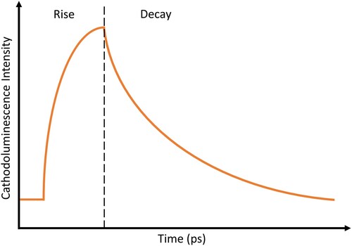
The pulsed electron beam can then use to excite the sample. In the time between pulses, the integrated intensity of the emitted photons is recorded producing a CL intensity decay transient. A representative CL intensity decay transient is shown in Figure which highlights the two main parts of the intensity variation being the rise and decay. The intensity rise occurs immediately after excitation and can be associated with any delaying processes that lengthen the diffusion distance of carriers towards recombination centres [Citation62]. The characteristic time taken for the CL intensity to reach maximum after excitation is the rise-time. During the decay part of the curve, the CL intensity decreases due to recombination processes that decrease the carrier concentration. The profile of the intensity decay can be exponential and is often analysed using single-, multi-, or stretched-exponential functions to extract a characteristic decay time which is often considered to be the effective carrier lifetime [Citation66, Citation67]. In such calculations, non-radiative recombination at surfaces is often ignored which can lead to underestimations [Citation68]. Usually, the behaviour of the intensity decay is complex and non-exponential. For instance, it can be non-linearly affected by the carrier density and depends on all the active recombination mechanisms in the material [Citation67]. In these hard to model cases, the time taken for the CL intensity to decay by can be used as a rough estimate for the carrier lifetime. The common detectors utilised for TRCL measurements are the time-correlated single-photon counting (TCSPC) and streak cameras. The detectors correlate a recorded photon with the time passed since reception of a trigger signal; usually the emission of the laser pulse plus a delay time to account for the non-relativistic travel speed of the beam electrons. Both detectors can offer temporal resolutions of a few picoseconds [Citation32]. It should be noted that the streak camera is typically operated in combination with a spectrometer producing datasets which simultaneously reveal the wavelength, time and intensity of the photons arriving at the detector [Citation61].
Figure 6. A representative cathodoluminescence decay transient. The figure highlights the cathodoluminescence intensity rise and intensity decay regions.
Applying TRCL to III-nitride semiconductors and devices
The subsequent sections will review how TRCL has been applied to unravelling phenomena that govern the properties of AlInGaN semiconductor materials and devices. The focus will be on the quantum-confined Stark effect in quantum wells and defect-related recombination pathways.
The quantum-confined stark effect
III-nitride LEDs and laser diodes (LDs) utilise double heterojunction quantum well (QW) structures. These QWs are formed by sandwiching a thin ( nm) film of a narrower band-gap active region semiconductor in between barrier layers of a wider band-gap semiconductor. It should be noted here that the QW is strained to the barrier layers due to lattice mismatch. The barrier layers provide an energy barrier that restricts diffusion out of the active region, spatially confining carriers within this film. Since the thickness of the active region is comparable to the de Broglie wavelength, quantum confinement occurs. This means that carriers are spatially confined to a two-dimensional plane that lies perpendicular to the thickness dimension of the QW.
As discussed in Section II A, the wz III-nitride phase possesses spontaneous polarisation fields. For the case of strained QWs, the non-centrosymmetry of the crystal also introduces additional piezoelectric polarisation fields. For the c-direction, which is the mature growth direction used in conventional planar QW LED designs, the polarisation fields act perpendicular to the plane of the active region – the c-plane. This effect modifies the electron and hole wavefunctions in the QW, spatially separating the carriers and reducing their overlap integral. In addition, the electron and hole energies states are shifted to lower and higher energies respectively which redshifts the emission and produces a sawtooth-like energy profile as can be seen in Figure . This redshifting of the emission energy as caused by an electric field is known as the quantum-confined Stark effect (QCSE) and the reduced overlap integral leads to a reduction in the optical emission efficiency of III-nitride LEDs and LDs.
Figure 7. (a) shows the energy profile and electron and hole wavefunctions in a QW with no polarisation fields. (b) is a polar III-nitride QW grown along the [0001] direction. Here the energy profile shows the quintessential sawtooth-like shape.
![Figure 7. (a) shows the energy profile and electron and hole wavefunctions in a QW with no polarisation fields. (b) is a polar III-nitride QW grown along the [0001] direction. Here the energy profile shows the quintessential sawtooth-like shape.](/cms/asset/1b1d6105-d96f-4368-b5a2-f9ffbccfdbd8/ymst_a_2064635_f0007_oc.jpg)
An important factor affecting the magnitude of the polarisation fields in QWs is the composition of the active region. For instance, increasing the InN content of InGaN QWs grown on GaN increases the magnitude of the polarisation fields, producing a greater carrier separation [Citation69]. The factors relevant to the QCSE in QWs such as quantum well width, composition, screening of polarisation fields and carrier localisation will now be discussed in terms of TRCL.
Quantum well width and composition
To investigate the effect of QW width and composition on the carrier dynamics of AlInGaN-based structures, a number of TRCL studies have been carried out. Metzner et al. [Citation70] explored InGaN QWs grown on the side facets of single pyramid GaN nanostructures with a hexagonal base as shown in Figure (a). The single pyramids were grown by MOVPE using self-assembly and showed six (11–22) facets. Using CL mapping, the peak InGaN QW emission energy was found to blueshift from the top (2.1 eV) of the pyramid to the base (2.25 eV) of the pyramid. Using this information, the authors rationalised that the top of the pyramid must have a thicker well width and/or higher InN concentration compared to the base of the pyramid. However, this assertion is not corroborated by direct measurements of the QW thickness variation and InN concentration which could have been performed using TEM and X-ray analysis respectively. Regardless, the authors observed faster CL decay transients for regions near the base of the pyramid compared to near the top as seen in Figure (b). It should be noted here that emission at the top persists for very long decay times beyond 30 ns. To rationalise this difference in decay times, consider the influence of the well thickness and InN concentration on the carrier separation within the QW. For the same QW thickness, regions of lower InN concentration should experience a smaller field and decreased carrier separation [Citation69]. For the same InN concentration, carriers in thinner QWs experience a decreased carrier separation [Citation71, Citation72]. In other words, there is less available distance for the carriers to separate. Hence, faster CL decay transients or shorter carrier lifetimes would imply thinner wells and/or lower InN concentration which would fit with the earlier assertion made through observation of the QW wavelength shift. However, it is important to also consider the effect of non-radiative recombination at defects which would decrease the lifetime of carriers and can lead to the differences observed. Regions where non-radiative recombination occurs can be observed as dark regions from CL intensity maps [Citation53, Citation73]. However, the authors did not provide this data, as such it is difficult to infer the influence of non-radiative recombination. In addition to being centres for non-radiative recombination, defects can also be radiative and affect the lifetime of carriers. The case of defect luminescence was highlighted by the authors who suggested that the very long lifetime observed near the top region was due to this effect. Although the authors make no attempt to identify this defect, it is possibly related to point defects that are associated with yellow luminescence (YL). YL is known to emit in the regime near 2.2 eV similarly to the top of the pyramid, which emits at 2.1 eV [Citation74].
Figure 8. (a) SEM image showing the GaN single pyramids on which InGaN QWs were grown. The green, blue and red squares indicate the respective base, facet and top regions where local CL spectra and decay transients were recorded. (b) shows the CL decay transients taken at the base and top of the single pyramid. The figures are reused from [Citation70]. © 2011 WILEY-VCH Verlag GmbH & Co. KGaA, Weinheim. All rights reserved.
![Figure 8. (a) SEM image showing the GaN single pyramids on which InGaN QWs were grown. The green, blue and red squares indicate the respective base, facet and top regions where local CL spectra and decay transients were recorded. (b) shows the CL decay transients taken at the base and top of the single pyramid. The figures are reused from [Citation70]. © 2011 WILEY-VCH Verlag GmbH & Co. KGaA, Weinheim. All rights reserved.](/cms/asset/ab8da428-f19e-4a43-a52f-969e40ba77f6/ymst_a_2064635_f0008_oc.jpg)
Defect recombination becomes especially important when considering the effect of lattice and thermal mismatch between the GaN and an overgrown InGaN layer. The defect density has been observed to increase with QW thickness for non-strain relaxed structures as they undergo strain relaxation [Citation75–77]. For the case of Metzner et al. [Citation70] above, it is possible that this is not a factor due to the microstructural nature of the QWs investigated. Nanostructure-based III-nitrides have been reported to carry less residual strain than the bulk material [Citation78–80]. Although the structures by Metzner et al. [Citation70] are not nanostructures, it is possible that their relatively small size could lead to strain relaxation. Hence, the defect density could be invariant with QW thickness.
The importance of considering defect-related recombination was shown by Corfdir et al. [Citation81]. The authors investigated InGaN QWs grown on (11–22) side facets of triangular prism shaped GaN structures. From the peak CL wavelength map in Figure (a), the authors observe a shift in the InGaN QW emission energy from 3.4 eV near the base of the prism to 3.05 eV at the top. The emission energy shift is associated with an increase in QW thickness. However, similar to Metzner et al. [Citation70], the authors do not provide any direct measurements of the QW thickness. In contrast to the data presented by Metzner et al. [Citation70], Corfdir et al. [Citation81] observe a decrease in the carrier lifetime with an assumed increase in QW thickness as seen in Figure (b). From Figure (a), dark spots, which are associated with threading dislocations, can be observed. The density of the spots is highest at the top of the prism where the QW is said to be thicker. Using this information, it was reasoned that the threading dislocation density increases with thickness leading to a reduction in the carrier lifetime. This is possibly due to the QW not being initially strain relaxed as the prisms in this case are relatively large.
Figure 9. (a) CL wavelength map of triangular prisms on which InGaN QWs were grown. The emission energy shifts from red (3.05 eV) at the top of the pyramid to blue (3.35 eV) at the base. (b) shows the CL decay transients taken at the base, face and top of the prism. The figures were reused from [Citation81]. © 2011 WILEY-VCH Verlag GmbH & Co. KGaA, Weinheim. All rights reserved.
![Figure 9. (a) CL wavelength map of triangular prisms on which InGaN QWs were grown. The emission energy shifts from red (3.05 eV) at the top of the pyramid to blue (3.35 eV) at the base. (b) shows the CL decay transients taken at the base, face and top of the prism. The figures were reused from [Citation81]. © 2011 WILEY-VCH Verlag GmbH & Co. KGaA, Weinheim. All rights reserved.](/cms/asset/151eb0fa-a1a9-47cd-9db6-2050f4943315/ymst_a_2064635_f0009_oc.jpg)
Screening of polarisation fields
The QCSE produces a redshift in the QW emission energy due to the sawtooth-like energy profile. With that said, the QW emission energy has been observed to blueshift with an increase in the charge carrier density as brought about by for instance an increase in the excitation level [Citation60]. The mechanism of polarisation field screening has been used to explain this blueshift [Citation82]. Here, the sheet charges at the opposite sides of the QW that manifest due to carrier separation are screened by an opposing sheet charge that forms due to excess charge carriers. The result is a flattening of the well's energy profile. Sala et al. [Citation82] point out that polarisation field screening can help rationalise some perplexing observations made regarding InGaN LDs such as their unusually high lasing threshold densities [Citation14]. The mechanism of band-filling can also be used to rationalise the observed blueshift. In this case, lower energy states are saturated with an increase in carrier density causing higher energy states to become populated [Citation83].
Using TRCL, Bell et al. [Citation23] investigated these effects on an InGaN QW with a nominal well width of 6 nm. At high carrier densities, the InGaN QW emission peak position blueshifts from its initial position in the first ns after turning the beam on and a redshift as soon as the beam is switched off. This can be seen in Figure . In another similar study, Bell et al. [Citation60] claim that both the effects of band filling and screening contribute to the observed blueshift akin to conclusions made by Chichibu et al. [Citation84]. In this similar study, Bell et al. [Citation60] examine TRCL intensity transients on InGaN QWs with a nominal width of 6 and 8 nm. They observe an initial fast decay in the time range 0–100 ns followed by a slower decay beyond 100 nm. The fast decay times were calculated to be 50 and 30 ns for the 6 and 8 nm wide QWs respectively. The slow decays were calculated to be 140 and 320 ns for the 6 and 8 nm wide QWs respectively. The fast initial decay is associated with polarisation field screening which improves the carrier recombination rate. This effect dominates initially due to the high initial carrier concentration. Interestingly, this initial fast decay is faster for the wider well. The authors attribute this to a greater initial charge carrier separation in the thicker QW which leads to an improved screening effect and faster recombination.
Figure 10. Variation in the InGaN QW emission peak position with time after TRCL excitation for different electron beam currents. The figure is reused from [Citation60]. © 2005 American Institute of Physics. All rights reserved.
![Figure 10. Variation in the InGaN QW emission peak position with time after TRCL excitation for different electron beam currents. The figure is reused from [Citation60]. © 2005 American Institute of Physics. All rights reserved.](/cms/asset/339e76ce-9ab9-40b7-9543-6ab461be0fce/ymst_a_2064635_f0010_ob.jpg)
Similarly to increasing the carrier concentration, doping the QW barriers can have a similar screening effect of the polarisation fields. Using TRCL, Jungclaus et al. [Citation24] studied GaN QWs with undoped and germanium doped AlN barriers. For the doped samples, the QW peak blueshifts by meV from its initial position of 3.6 eV in the first 5 ns after excitation. In this case, polarisation field screening is corroborated by an observed decrease in the carrier lifetime with doping. The decrease in carrier lifetime can again be rationalised by a reduced carrier separation.
Carrier localisation
Even though the QCSE is expected to decrease the optical emission efficiency of AlInGaN-based QWs, III-nitride LEDs such as those of InGaN still show a surprisingly high efficiency. This is uncanny especially when accounting for the usually high threading dislocation density [Citation85]. The threading dislocations are expected to act as centres of non-radiative recombination similar to observations made by Corfdir et al. in Figure (a). The expected result is a limited optical efficiency. Nonetheless, when compared to their arsenide counterparts (GaAs or AlGaAs), the efficiency of III-nitride LEDs and LDs is largely unaffected by the dislocation density [Citation86]. This effect is commonly attributed to localisation of carriers [Citation86–88]. Instead of diffusing to, being trapped by, and recombining non-radiatively at threading dislocation defect states, the carriers recombine radiatively at localisation centres. Several mechanisms by which carrier localisation occurs have been suggested including; QW thickness fluctuations and random alloy fluctuations.
The effect of QW thickness fluctuations on carrier localisation was studied by Sonderegger et al. [Citation89] using TRCL. The authors compared the lateral morphology of an InGaN/GaN QW as obtained using atomic force microscopy (AFM), shown in Figure (a), with monochromatic CL intensity maps, of the same region, taken at the higher (3.13 eV) and lower energy (3.07 eV) tails of the InGaN QW emission peak, shown in Figure (b) and (c). From Figure , it can be seen that the intensity distribution of the higher energy tail was found to correspond to valleys(I) on the QW surface whilst the lower energy tail matched with ridges(II). This correlation allowed the authors to deduce that the valleys are potential energy maxima while the ridges are consistent with potential minima. This assertion was corroborated by TRCL data. A pronounced redshift ( meV) of the QW peak with time was observed for the valley regions, as seen in Figure (a), compared to the hill regions in (b). The redshift is attributed to diffusion of carriers from the higher energy valleys to the potential minima within the hill regions. However, the redshift can also be justified by an initially high carrier density producing an initially blueshifted InGaN QW peak because of polarisation field screening. After some ps, the peak will redshift with time as the carrier density decreases similar to Jungclaus et al. [Citation24] and Bell et al. [Citation23]. The authors refute the effect of polarisation field screening by estimating that the initial carrier density is too low to have a substantial effect on the peak position. Although not pointed out by the authors, a low carrier density would also eliminate any blueshifts caused by band-filling [Citation90]. In addition, the authors argue that the nominal QW thickness of 1.5 nm is too small to produce a sufficient polarisation field induced redshift which is consistent with the literature [Citation91].
Figure 11. (a) AFM image of the surface of an InGaN/GaN QW. (b) monochromatic CL map of the same surface in (a) taken at 3.13 eV. (c) monochromatic CL map of the same surface in (a) taken at 3.07 eV. The figure is reused from [Citation89]. © 2005 American Institute of Physics. All rights reserved.
![Figure 11. (a) AFM image of the surface of an InGaN/GaN QW. (b) monochromatic CL map of the same surface in (a) taken at 3.13 eV. (c) monochromatic CL map of the same surface in (a) taken at 3.07 eV. The figure is reused from [Citation89]. © 2005 American Institute of Physics. All rights reserved.](/cms/asset/25c2b5dc-2476-4bb2-8517-b9ac9872f381/ymst_a_2064635_f0011_oc.jpg)
Figure 12. (a) Streak camera image taken in the valley region. (b) Streak camera image taken in the hill regions. The colour scale represents intensity in arbitrary units. The figure is reused from [Citation89]. © 2005 American Institute of Physics. All rights reserved.
![Figure 12. (a) Streak camera image taken in the valley region. (b) Streak camera image taken in the hill regions. The colour scale represents intensity in arbitrary units. The figure is reused from [Citation89]. © 2005 American Institute of Physics. All rights reserved.](/cms/asset/55ac794c-ffed-418e-9388-92a555c467ab/ymst_a_2064635_f0012_oc.jpg)
Carrier localisation has been said to also occur at random alloy fluctuations. The fluctuations can for instance create InN-rich and GaN-rich regions in an InGaN QW. This leads to the creation of potential energy minima and maxima. Several authors have claimed to observe these regions as adjacent regions of dark and bright contrast in monochromatic CL intensity maps [Citation23, Citation25] and as adjacent regions of low and high energy in CL wavelength maps [Citation92]. However, the size of the clusters observed from CL maps is of the order of micrometres which is contrary to established work which proposes that the size of the fluctuations is of the order of a few nanometres [Citation85]. Due to the limitations brought about by carrier diffusion and the interaction volume, such features, of size in the few nanometres, would be difficult to resolve using CL, see Section IV A.
Using TRCL, Zhang et al. [Citation25] found that microclusters which corresponded to the lower energy end of the InGaN peak centred at 410 nm showed a longer carrier lifetime than those that corresponded to the higher energy end. Similar observations were also made by Rudloff et al. [Citation92]. If indeed the microclusters observed here represented InGaN compositional fluctuations as reported by the authors, then a shorter carrier lifetime would be expected for the lower energy regions. Although Zhang et al. [Citation25] reasoned that their peculiar results were due to non-radiative recombination at defects localised at higher energy nanoclusters, still, such conclusions cannot be made purely from CL and TRCL data. First, the authors could have provided X-ray analysis data to ascertain that indeed the variation in emission energy is due to a variation in the InGaN composition. Second, TEM could have aided in determining any variations in the extended defect density. Lastly, the authors failed to consider other factors that could explain the observations made such as QW thickness variations which were shown by Sonderegger et al. [Citation89] to be in the same micrometre lengthscale.
Defect-related carrier recombination channels
Understanding the recombination channels taken by excess carriers from generation to recombination is critical for device optimisation. For instance, this can help in unravelling the origin of defect luminescence bands, the competition between radiative and non-radiative recombination centres, and the specific diffusion paths taken by excess carriers [Citation26, Citation74, Citation93]. The focus of this section will be to summarise TRCL work related to defect-associated carrier recombination with a focus on point defects and stacking faults.
Point defects
Point defect luminescence bands have been observed in the emission spectra of III-nitrides [Citation74, Citation94]. Their presence shows that there exists competing radiative recombination pathways to that of the band-edge emission.
The yellow luminescence (YL) band, which appears as a broad peak centred near 2.2 eV has remained controversial with regards to its origin in the literature. For instance, it has been related to transitions from shallow level donors or the conduction band edge to deep level acceptors, but has also been associated with transitions from a shallow level donor to a shallow level acceptor [Citation74]. Diaz-Guerra et al. [Citation74] have found that this broad peak can be resolved into at least five components. CL decay transients taken about these respective peaks were fully described by a single-exponential with carrier lifetimes in the 100 μs regime and showing a narrow distribution of values. To rationalise these results, the authors considered the Thomas-Hopfield model for the recombination of donor-acceptor pairs [Citation95]. The model proposes that the rate of recombination of carriers depends on the separation of donors and acceptors [Citation95]. Thus recombination that is mediated by donor–acceptor pairs in close proximity will have a shorter associated lifetime than those further apart. In this case, a larger scatter of lifetime values and a nonexponential decay character is expected. However, this is not the case from the experimental data. Instead, the authors reason that the observed behaviour is best described by associating the YL to transitions involving deep levels and the conduction band instead of donor–acceptor pairs [Citation74, Citation96].
Another study related to point defect relaxation was carried out by Fischer et al. [Citation94]. The authors studied the behaviour of the donor–acceptor pair (DAP) band in Mg-doped GaN films. They compared the CL decay transients of the DAP centre wavelength ( eV) with that of its first-order longitudinal-optical (1LO) phonon replica (
eV). At low Mg concentrations, the decay behaviours for both processes are similar. However, a deviation is observed when the Mg concentration is increased. This is an interesting result since the behaviour of the DAP and its 1LO phonon replica is expected to be similar. By observing the change in the emission wavelength with time, a redshift was observed for both the DAP and 1LO phonon replica. Using the Thomas–Hopfield model [Citation95], the authors relate the redshift to a progressive increase in the distance between the recombining donor–acceptor pairs. However, similarly to the decay behaviour, the redshift for both is not identical being 0.05 eV for the DAP and 0.025 eV for the 1LO phonon replica. The authors use these discrepancies to argue the existence of some secondary recombination channel that emits within the investigated wavelength range.
Stacking faults
To understand radiative recombination channels, Corfdir et al. [Citation26] studied regions of high and low basal stacking fault (BSF) density in GaN. The authors observed a slow rise-time in the CL intensity decay transients for BSFs compared to that of free excitons (FX) when the electron beam was placed at a region of low stacking fault density as seen in Figure . This slower rise-time is unexpected as the BSFs are anticipated to either be directly excited by the electron beam or to capture free excitons that are directly excited in the spaces between BSFs. However, by considering the capture of free excitons by donors this result can be rationalised as follows. Free excitons generated by the electron beam in the spaces between BSFs are captured by donors and thermally reemitted which is followed by capture at a neighbouring donor. This donor hopping process occurs until the excitons reach a BSF and recombine radiatively [Citation26, Citation93]. The hopping process increases the diffusion distance of excitons towards BSFs bringing about the slower rise-time. Such exciton hopping processes are expected to dominate in bulk GaN for instance when compared to confinement structures such as QWs. This is because of exciton localisation at potential minima induced by QW thickness variations and compositional fluctuations as previously discussed in Section V A 3.
Figure 13. Figure shows the CL intensity transients of free excitons (FX), donor-bound excitons (DX), and BSF excitons when excitation is carried in a region of low BSF density. The insert highlights the calculated spatial distributions (n) of FX and D
X at
(squares) and
ps (triangles). The figure is reused from [Citation26]. © 2005 American Institute of Physics. All rights reserved.
![Figure 13. Figure shows the CL intensity transients of free excitons (FX), donor-bound excitons (D∘X), and BSF excitons when excitation is carried in a region of low BSF density. The insert highlights the calculated spatial distributions (n) of FX and D∘X at t=0 (squares) and t=50 ps (triangles). The figure is reused from [Citation26]. © 2005 American Institute of Physics. All rights reserved.](/cms/asset/87011335-41cd-4174-985c-600a86fcfe52/ymst_a_2064635_f0013_oc.jpg)
Conclusion
The AlInGaN family of semiconductors is technologically important for the design of optoelectronic devices such as LEDs and LDs. Thus it is crucial to have a firm grasp of the underlying phenomena that govern the properties of these materials and their devices. The charge carrier dynamics, which relates to the activity and behaviour of charge carriers in the period between generation and recombination, is one such phenomenon that deserves consideration. Investigation of the charge carrier dynamics can be performed using TRCL. Here, a picosecond pulsed electron beam is used to excite excess charge carriers. The datasets obtained, such as CL intensity transients, can be used to make conclusions about the properties of the materials and devices from the point of view of carrier dynamics. When applied to the study of AlInGaN QWs, TRCL was shown to be able to unravel a multitude of properties especially those related to the QCSE. It was shown that changes in CL intensity decay times could help in understanding the effects of thickness fluctuations, composition, polarisation field screening and carrier localisation on the properties of QWs. However, care must be taken to not over-interpret the data. For instance, CL on its own cannot be used to make conclusions regarding the existence of thickness and compositional variations. In addition, when analysing the CL intensity transients, the effect of non-radiative recombination should always be considered. TRCL was also shown to be applicable in resolving defect-associated carrier recombination channels such as those associated with point defects and stacking faults.
Declaration
This review is the author's own work. Any assistance has been noted in the acknowledgements section.
Acknowledgments
The author would like to acknowledge the government of Botswana for funding his Ph.D. studies. The author would also like to extend his thanks to Prof. Rachel Oliver for her support along with Dr. Gunnar Kusch for the useful discussions and proofreading the document.
Disclosure statement
No potential conflict of interest was reported by the author.
References
- Nakamura S. Background story of the invention of efficient InGaN blue-light-emitting diodes (nobel lecture). Angew Chem Int Ed. 2015;54:7770–7788.
- Nakamura S, Mukai T, Senoh M. Candela-class high-brightness InGaN/AlGaN double-heterostructure blue-light-emitting diodes. Appl Phys Lett. 1994;64:1687–1689.
- Funato M, Ueda M, Kawakami Y, et al. Blue, green, and amber InGaN/GaN light-emitting diodes on semipolar {11–22} GaN bulk substrates. Jpn J Appl Phys. 2006;45:L659–L662.
- Nakamura S, Senoh M, Iwasa N, et al. High-brightness InGaN blue, green and yellow light-emitting diodes with quantum well structures. Jpn J Appl Phys. 1995;34:L797–L799.
- Nakamura S, Senoh M, Iwasa N, et al. Superbright green InGaN single-quantum-well-structure light-emitting diodes. Jpn J Appl Phys. 1995;34:L1332–L1335.
- Kato H, Sugitani C. Wide gamut display using LED backlight – technical developments and actual products. NEC Tech J. 2006;1:75–79.
- Mukai T, Yamada M, Nakamura S. Characteristics of InGaN-based UV/blue/green/amber/red light-emitting diodes. Jpn J Appl Phys. 1999;38:3976–3981.
- Jain SC, Willander M, Narayan J, et al. III-nitrides: growth, characterization, and properties. J Appl Phys. 2000;87:965–1006.
- Krames MR, Shchekin OB, Mueller-Mach R, et al. Status and future of high-power light-emitting diodes for solid-state lighting. J Disp Technol. 2007;3:160–175.
- Ma J, Zhu X, Wong KM, et al. Improved GaN-based LED grown on silicon (111) substrates using stress/dislocation-engineered interlayers. 16th International Conference on Metalorganic Vapor Phase Epitaxy. 2013;370:265–268.
- Orton JW, Foxon CT. Group III nitride semiconductors for short wavelength light-emitting devices. Rep Prog Phys. 1998;61:1–75.
- Kavehrad M. Sustainable energy-efficient wireless applications using light. IEEE Commun Mag. 2010;48:66–73.
- Nishimura K, Shimizu K, Shibahara Y, et al. 59.1: invited paper: on the recent progress of LED lighting in japan. SID Symposium Digest of Technical Papers. 2010;41:878–881.
- Nakamura S, Senoh M, Nagahama S-I, et al. InGaN-based multi-quantum-well-structure laser diodes. Jpn J Appl Phys. 1996;35:L74–L76.
- Jani O, Ferguson I, Honsberg C, et al. Design and characterization of GaNInGaN solar cells. Appl Phys Lett. 2007;91:132117.
- Yang H, Ma Z, Jiang Y, et al. The enhanced photo absorption and carrier transportation of InGaN/GaN quantum wells for photodiode detector applications. Sci Rep. 2017;7:43357.
- Strite S, Morkoç H. GaN, AlN, and InN: a review. J Vacuum Sci Technol B Microelectron Nanometer Struct Process Measure Phenomena. 1992;10:1237–1266.
- Feneberg M, Leute RAR, Neuschl B, et al. High-excitation and high-resolution photoluminescence spectra of bulk AlN. Phys Rev B. 2010;82:075208.
- Davydov V, Klochikhin A, Seisyan R, et al. Absorption and emission of hexagonal InN. evidence of narrow fundamental band gap. Phys Status Solidi B. 2002;229:r1–r3.
- Nishida T, Saito H, Kobayashi N. Efficient and high-power AlGaN-based ultraviolet light-emitting diode grown on bulk GaN. Appl Phys Lett. 2001;79:711–712.
- Taniyasu Y, Kasu M, Makimoto T. An aluminium nitride light-emitting diode with a wavelength of 210 nanometres. Nature. 2006;441:325–328.
- Mondal RK, Adhikari S, Chatterjee V, et al. Recent advances and challenges in AlGaN-based ultra-violet light emitting diode technologies. Mater Res Bull. 2021;140:111258.
- Bell A, Christen J, Bertram F, et al. Localization versus carrier-screening effects in InGaN quantum wells – A time-resolved cathodoluminescence study. AIP Conf Proc. 2005;772:301–302.
- Jungclaus J, Spende H, Hille P, et al. Time-resolved cathodoluminescence investigations of AlN:Ge/GaN nanowire structures. Nano Express. 2021;2:034001.
- Zhang X, Rich DH, Kobayashi JT, et al. Carrier relaxation and recombination in an InGaN/GaN quantum well probed with time-resolved cathodoluminescence. Appl Phys Lett. 1998;73:1430–1432.
- Corfdir P, Ristić J, Lefebvre P, et al. Low-temperature time-resolved cathodoluminescence study of exciton dynamics involving basal stacking faults in a-plane GaN. Appl Phys Lett. 2009;94:201115.
- Zhu T, Gachet D, Tang F, et al. Local carrier recombination and associated dynamics in m-plane InGaN/GaN quantum wells probed by picosecond cathodoluminescence. Appl Phys Lett. 2016;109:232103.
- Miwa H, Gong X, Hashimoto A, et al. Nanoscale photoluminescence mapping for MOVPE InN films using scanning near-field optical microscopy (SNOM). Sci Technol Adv Mater. 2006;7:282–285.
- Liuolia V, Pinos A, Marcinkevičius S, et al. Carrier localization in m-plane InGaN/GaN quantum wells probed by scanning near field optical spectroscopy. Appl Phys Lett. 2010;97:151106.
- Feng Z, Jiang X, Lee Y. Green light-emitting diodes with InGaN/GaN multiple quantum well structures: Time-resolved photoluminescence, emission dynamics and related studies.2016 5th International Symposium on Next-Generation Electronics2016.
- Li C, Stokes E, Hefti R, et al. PL spatial variation in InGaN/GaN MQWs studied by confocal microscopy and TRPL spectroscopy. ECS J Solid State Sci Technol. 2013;2:R262–R266.
- Onuma T, Kagamitani Y, Hazu K, et al. Femtosecond-laser-driven photoelectron-gun for time-resolved cathodoluminescence measurement of GaN. Rev Sci Instrum. 2012;83:043905.
- Goldstein JI, Newbury DE, Echlin P, et al. The SEM and its modes of operation. In: Goldstein JI, Newbury DE, Echlin P, Joy DC, Lyman CE, Lifshin E, Sawyer L, and Michael JR, editors. Scanning electron microscopy and X-ray microanalysis. 3rd ed. Boston, MA: Springer US; 2003. p. 21–60.
- Coenen T, Haegel NM. Cathodoluminescence for the 21st century: learning more from light. Appl Phys Rev. 2017;4:031103.
- Ferreyra RA, Zhu C, Teke A, et al. Group III Nitrides. . In: Kasap S, Capper P, editors. Springer Handbook of Electronic and Photonic Materials. Springer, Cham; 2017. p. 1.
- Frentrup M, Lee LY, Sahonta S-L, et al. X-ray diffraction analysis of cubic zincblende III-nitrides. J Phys D: Appl Phys. 2017;50:433002.
- Ambacher O, Majewski J, Miskys C, et al. Pyroelectric properties of Al(In)GaN/GaN hetero- and quantum well structures. J Phys: Condens Matter. 2002;14:3399–3434.
- Schubert MF, Chhajed S, Kim JK, et al. Effect of dislocation density on efficiency droop in GaInNGaN light-emitting diodes. Appl Phys Lett. 2007;91:231114.
- Yam FK. Gallium nitride: an overview of structural defects. In: Low LL and Oh SA, editors. Optoelectronics. Rijeka: IntechOpen; 2011. Ch. 4.
- Suemitsu M, Filimonov S. Understanding crystal growth mechanisms in silicon–germanium (SiGe) nanostructures. In: Shiraki Yasuhiro, Usami Noritaka, editors. Silicon–Germanium (SiGe) Nanostructures.Woodhead Publishing; 2011. p. 45–71.
- Zubialevich VZ, McLaren M, Pampili P, et al. Reduction of threading dislocation density in top-down fabricated GaN nanocolumns via their lateral overgrowth by MOCVD. J Appl Phys. 2020;127:025306.
- Johnson M, Yu Z, Brown J, et al. A critical comparison between MOVPE and MBE growth of III-V nitride semiconductor materials for opto-electronic device applications. MRS Int J Nitride Semicond Res. 1999;4:594–599.
- Dumke WP. Spontaneous radiative recombination in semiconductors. Phys Rev. 1957;105:139–144.
- Wannier GH. The structure of electronic excitation levels in insulating crystals. Phys Rev. 1937;52:191–197.
- Muth JF, Lee JH, Shmagin IK, et al. Absorption coefficient, energy gap, exciton binding energy, and recombination lifetime of GaN obtained from transmission measurements. Appl Phys Lett. 1997;71:2572–2574.
- Götz W, Johnson N, Chen C, et al. Activation energies of Si donors in GaN. Appl Phys Lett. 1996;68:3144–3146.
- Lee I-H, Polyakov AY, Smirnov NB, et al. Point defects controlling non-radiative recombination in GaN blue light emitting diodes: insights from radiation damage experiments. J Appl Phys. 2017;122:115704.
- Xie Z, Sui Y, Buckeridge J, et al. Donor and acceptor characteristics of native point defects in GaN. J Phys D Appl Phys. 2019;52:335104.
- Shockley W, Read WT. Statistics of the recombinations of holes and electrons. Phys Rev. 1952;87:835–842.
- Haug A. Auger recombination in direct-gap semiconductors: band-structure effects. J Phys C Solid State Phys. 1983;16:4159–4172.
- Meyer J, Liu R, Schaller RD, et al. Systematic study of shockley-read-hall and radiative recombination in GaN on Al2O3, freestanding GaN, and GaN on Si. J Phys Photon. 2020;2:035003.
- Reshchikov MA. Chapter Nine - Point Defects in GaN. In: Romano Lucia, Jagadish Chennupati, Privitera Vittorio, editors. Semiconductors and Semimetals Vol. 91 Elsevier; 2015. p. 315–367.
- Yacobi BG, Holt DB. Cathodoluminescence scanning electron microscopy of semiconductors. J Appl Phys. 1986;59:R1–R24.
- Meuret S, Tizei LHG, Houdellier F, et al. Time-resolved cathodoluminescence in an ultrafast transmission electron microscope. Appl Phys Lett. 2021;119:062106.
- Phillips MR. Cathodoluminescence microscopy and spectroscopy of opto-Electronic materials. Microchim Acta. 2006;155:51–58.
- Kanaya K, Okayama S. Penetration and energy-loss theory of electrons in solid targets. J Phys D: Appl Phys. 1972;5:43–58.
- Ishikawa Y, Tashiro M, Hazu K, et al. Local lifetime and luminescence efficiency for the near-band-edge emission of freestanding GaN substrates determined using spatio-time-resolved cathodoluminescence. Appl Phys Lett. 2012;101:212106.
- Modak S, Chernyak L, Xian M, et al. Impact of electron injection on carrier transport and recombination in unintentionally doped GaN. J Appl Phys. 2020;128:085702.
- Fonoberov VA, Balandin AA. Origin of ultraviolet photoluminescence in ZnO quantum dots: confined excitons versus surface-bound impurity exciton complexes. Appl Phys Lett. 2004;85:5971–5973.
- Bell A, Christen J, Bertram F, et al. Localization versus field effects in single InGaN quantum wells. Appl Phys Lett. 2004;84:58–60.
- Merano M, Sonderegger S, Crottini A, et al. Probing carrier dynamics in nanostructures by picosecond cathodoluminescence. Nature. 2005;438:479–482.
- Merano M, Sonderegger S, Crottini A, et al. Time-resolved cathodoluminescence of InGaAs/AlGaAs tetrahedral pyramidal quantum structures. Appl Phys B. 2006;84:343–350.
- Ura K, Fujioka H, Hosokawa T. Picosecond pulse stroboscopic scanning electron microscope. J Electron Microsc (Tokyo). 1978;27:247–252.
- Moerland RJ, Weppelman IGC, Garming MWH, et al. Time-resolved cathodoluminescence microscopy with sub-nanosecond beam blanking for direct evaluation of the local density of states. Opt Express. 2016;24:24760–24772.
- Meuret S, Solà Garcia M, Coenen T, et al. Complementary cathodoluminescence lifetime imaging configurations in a scanning electron microscope. Ultramicroscopy. 2019;197:28–38.
- Chichibu S, Ishikawa Y, Hazu K, et al. Spatio-time-resolved cathodoluminescence studies of wide bandgap group-III nitride semiconductors. Jpn J Appl Phys. 2019, DOI:10.7567/1347-4065/ab5ef4.
- Hangleiter A. Recombination dynamics in GaInN/GaN quantum wells. Semicond Sci Technol. 2019;34:073002.
- Weiss TP, Bissig B, Feurer T, et al. Bulk and surface recombination properties in thin film semiconductors with different surface treatments from time-resolved photoluminescence measurements. Sci Rep. 2019;9:5385.
- Wang T. Topical review: development of overgrown semi-polar GaN for high efficiency green/yellow emission. Semicond Sci Technol. 2016;31:093003.
- Metzner S, Bertram F, Karbaum C, et al. Spectrally and time-resolved cathodoluminescence microscopy of semipolar InGaN SQW on (11–22) and (10–11) pyramid facets. Phys Status Solidi B. 2011;248:632–637.
- Bai J, Wang T, Sakai S. Influence of the quantum-well thickness on the radiative recombination of InGaN/GaN quantum well structures. J Appl Phys. 2000;88:4729–4733.
- Shapiro NA, Perlin P, Kisielowski C, et al. The effects of indium concentration and well-thickness on the mechanisms of radiative recombination in InxGa1xN quantum wells. MRS Internet J Nitride Semicond Res. 2020;5:2.
- He S, Xu Y, Qi L, et al. Growth of low-threading-dislocation-density GaN on graphene by hydride vapor phase epitaxy. Jpn J Appl Phys. 2017;56:030308.
- Dıaz-Guerra C, Piqueras J, Castaldini A, et al. Time-resolved cathodoluminescence and photocurrent study of the yellow band in Si-doped GaN. J Appl Phys. 2003;94:2341–2346.
- Redaelli L, Mukhtarova A, Valdueza-Felip S, et al. Effect of the quantum well thickness on the performance of InGaN photovoltaic cells. Appl Phys Lett. 2014;105:131105.
- Yoshizumi Y, Yoshida T, Kyono T. Advantages of employing the freestanding GaN substrates with low dislocation density for white light-emitting diodes. SEI Tech Rev. 2012:110–115.
- Wei T, Zhang L, Ji X, et al. Investigation of efficiency and droop behavior comparison for InGaN/GaN super wide-well light emitting diodes grown on different substrates. IEEE Photonics J. 2014;6:1–10.
- Wang Q, Bai J, Gong YP, et al. Influence of strain relaxation on the optical properties of InGaN/GaN multiple quantum well nanorods. J Phys D Appl Phys. 2011;44:395102.
- Ley R, Chan L, Shapturenka P, et al. Strain relaxation of InGaN/GaN multi-quantum well light emitters via nanopatterning. Opt Express. 2019;27:30081–30089.
- Avit G, Robin Y, Liao Y, et al. Strain-induced yellow to blue emission tailoring of axial InGaN/GaN quantum wells in GaN nanorods synthesized by nanoimprint lithography. Sci Rep. 2021;11:6754.
- Corfdir P, Simeonov D, Feltin E, et al. Time-resolved cathodoluminescence on polychromatic light emitting (In, Ga)N quantum wells grown on (11-22) GaN facets. Phys Status Solidi C. 2011;8:1394–1397.
- Della Sala F, Di Carlo A, Lugli P, et al. Free-carrier screening of polarization fields in wurtzite GaN/InGaN laser structures. Appl Phys Lett. 1999;74:2002–2004.
- Weng G, Zhao W-R, Chen S, et al. Strong localization effect and carrier relaxation dynamics in self-assembled InGaN quantum dots emitting in the green. Nanoscale Res Lett. 2015;10.
- Chichibu S, Azuhata T, Sota T, et al. Spontaneous emission of localized excitons in InGaN single and multiquantum well structures. Appl Phys Lett. 1996;69:4188–4190.
- Oliver RA, Bennett SE, Zhu T, et al. Microstructural origins of localization in InGaN quantum wells. J Phys D: Appl Phys. 2010;43:354003.
- Akasaka T, Gotoh H, Kobayashi Y, et al. InGaN quantum wells with small potential fluctuation grown on InGaN underlying layers. Appl Phys Lett. 2006;89:101110.
- Badcock TJ, Dawson P, Davies MJ, et al. Low temperature carrier redistribution dynamics in InGaN/GaN quantum wells. J Appl Phys. 2014;115:113505.
- Arteev DS, Sakharov AV, Zavarin EE, et al. Investigation of statistical broadening in InGaN alloys. J Phys: Conf Ser. 2018;1135:012050.
- Sonderegger S, Feltin E, Merano M, et al. High spatial resolution picosecond cathodoluminescence of InGaN quantum wells. Appl Phys Lett. 2006;89:232109.
- Jiao QQ, Chen ZZ, Ma J, et al. Capability of GaN based micro-light emitting diodes operated at an injection level of kA/cm2. Opt Express. 2015;23:16565–16574.
- Hou X, Fan S, Iida D, et al. Photoluminescence of InGaN-based red multiple quantum wells. Opt Express. 2021;29:30237–30243.
- Rudloff D, Bertram F, Riemann T, et al. Direct imaging of the crystalline and chemical nanostructure of GA, IN-nitrides by highly spatially-, spectrally- and time-resolved cathodoluminescence. Solid State Phenom. 1998;63–64:221–228.
- Corfdir P, Lefebvre P, Balet L, et al. Exciton recombination dynamics in a-plane (Al, Ga)N/GaN quantum wells probed by picosecond photo and cathodoluminescence. J Appl Phys. 2010;107:043524.
- Fischer AM, Srinivasan S, Ponce FA, et al. Time-resolved cathodoluminescence of Mg-doped GaN. Appl Phys Lett. 2008;93:151901.
- Thomas DG, Hopfield JJ, Augustyniak WM. Kinetics of radiative recombination at randomly distributed donors and acceptors. Phys Rev. 1965;140:A202–A220.
- Dıaz-Guerra C, Piqueras J, Cavallini A. Time-resolved cathodoluminescence assessment of deep-level transitions in hydride-vapor-phase-epitaxy GaN. Appl Phys Lett. 2003;82:2050–2052.