Abstract
The possibility that GaN charged nanoparticles might be generated during the synthesis of GaN nanostructures was examined in an atmospheric-pressure chemical vapor deposition (CVD) process using a differential mobility analyzer combined with a Faraday cup electrometer. Both positively and negatively charged nanoparticles in the size range of 10–100 nm were generated in the reactor of the CVD process using Ga2O3 precursor and NH3 gas. With decreasing flow rate of NH3 from 400 to 0 standard cubic centimeter per min (sccm) and decreasing reactor temperature from 1100°C to 500°C, the size and the number concentration of charged nanoparticles decreased. As the size and the number density decreased, the size of deposited GaN hexagonal crystals decreased and eventually GaN nanowires began to grow without catalysts.
Copyright 2012 American Association for Aerosol Research
1. INTRODUCTION
In the past decades, GaN, a wide band gap material of ∼3.4 eV, which belongs to prospective III-nitride semiconductors (Ambacher 1998), has attracted great scientific and technological interests because of the good electrical and thermal stability (Ambacher 1998; Neudeck et al. 2002; Hudgins et al. 2003), and its light emitting characteristic in a wide range beyond the visible light. Besides, it has good doping characteristics, high carrier mobility, and large peak velocity which are essential for the high frequency devices. Because of these excellent physical properties, GaN nanostructures have potential applications in ultraviolet (UV) or blue photon emitters for light emitting diodes (LEDs) (Orton and Foxon 1998), high-speed field effect transistors of optical telecommunications (Mishra et al. 2002), and high temperature/high power electronic devices for automobile applications (Neudeck et al. 2002).
GaN films or nanostructures have been synthesized by various chemical vapor deposition (CVD) processes, such as atmospheric-pressure CVD (Han et al. Citation1997), plasma-enhanced CVD (Choi et al. Citation1993), metal-organic CVD (Amano et al. Citation1986), and hot-wire CVD (Yasui et al. Citation2003; Peng et al. Citation2000). In spite of extensive researches, the role of process parameters in the deposition behavior has not been clearly understood. For example, it is not understood why films grow under certain conditions and nanowires grow under other conditions.
Recently, Hwang et al. (Hwang et al. Citation1996; Hwang Citation1999; Jeon et al. Citation2000; Lee et al. Citation2001, Citation2002b, Citation2008; Hwang and Kim Citation2004; Kim et al. Citation2006; Hwang and Lee Citation2010) suggested that charged nanoparticles are usually generated in the gas phase during the CVD process and play an important role in the microstructure evolution of films or nanostructures. Using a differential mobility analyzer (DMA) or other particle detecting systems attached to a CVD reactor, Adachi et al. (Adachi et al. Citation1992, 1993, Citation1995, Citation1996) made an extensive study that a huge amount of SiO2 nanoparticles are generated in the gas phase almost unavoidably under the deposition condition of SiO2 films. Later, the generation of charged nanoparticles in the gas phase was experimentally confirmed under the deposition condition of films or nanostructures in many other CVD processes. For example, the generation of charged nanoparticles was confirmed during the syntheses of diamond films (Hwang Citation1999; Jeon et al. Citation2000; Ahn et al. Citation2002), zirconia films (Jeon et al. Citation2001a), copper films (Lee et al. Citation2002a), silicon films (Cheong et al. Citation1999; Lee et al. Citation2008; Kim et al. Citation2010b), silicon nanowires (Kim et al. Citation2010a), ZnO nanowires (Kim et al. Citation2009a) and carbon nanotubes (Kim et al. Citation2009b; Lee and Hwang Citation2008).
The possibility of generation of charged nanoparticles in the gas phase and their deposition into films during CVD was originally suggested to explain the puzzling experimental fact that diamond is deposited on graphite, which is being etched away. This well-known phenomenon of simultaneous deposition of less stable diamond and etching of stable graphite violates the second law of thermodynamics if the deposition is done by atomic unit and is called “thermodynamic paradox” (Banholzer Citation1992; Yarbrough Citation1992; Hwang and Yoon Citation1996; Piekarczyk Citation1998). Hwang and Yoon (Citation1996) suggested that if the diamond nuclei are formed in the gas phase in the CVD process, both graphite and diamond should be etched away because the C-H binary system has a retrograde solubility of carbon in the gas phase around the substrate temperature. Further, they suggested that if the gas phase nuclei should deposit into diamond films, the phenomenon of simultaneous diamond deposition and graphite etching should be free of thermodynamic paradox. According to this suggestion, diamond films should grow 100% by gas phase nuclei because atomically both diamond and graphite should be etched away.
It is well known that diamond crystals grow on a Si substrate but highly porous skeletal soot particles grow on a Fe substrate under the same deposition condition (Hahn et al. Citation1996). In order to explain this puzzling phenomenon, Hwang et al. (Citation1996) suggested that diamond gas phase nuclei are negatively charged. When charged diamond nuclei approach an Fe substrate, they lose charge and transform to graphite, producing a skeletal porous soot structure on an Fe substrate. When charged diamond nuclei approach a Si substrate, however, they undergo colloidal crystallization, producing void-free diamond films on the Si substrate. Later, the generation of charged diamond gas phase nuclei was experimentally confirmed in a series of experiments (Hwang Citation1999; Jeon et al. Citation2000; Ahn et al. Citation2002).
The growth of diamond crystals solely by charged gas phase nuclei has many important implications. First, diamond crystals should grow by the colloidal crystallization in the gas phase. The electrostatic energy arising from the charged nuclei should be responsible for the self-assembly. Second, the atomic diffusion should be enhanced remarkably by the presence of charge, judging from the fact that void-free crystals can grow by the building block of charged nanoparticles. Third, the diffusion enhanced by charge depends on the number of atoms per charge or the size of the charged nanoparticles, judging from the fact that small charged nuclei produced diamond crystals with well-defined facets whereas large ones produced ball-like or cauliflower structures (Jeon et al. Citation2001b).
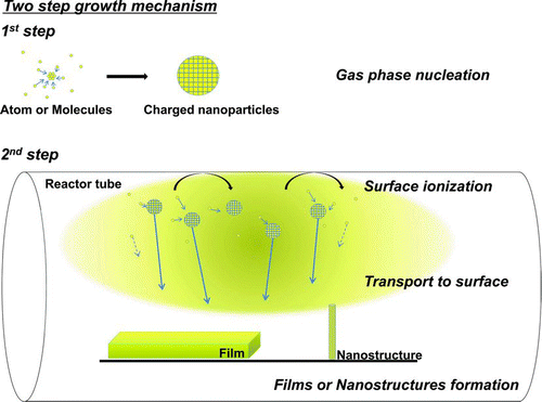
Then, a question arises as to whether this mechanism of film growth is unique to diamond or more generally applicable to others elements or compounds. In order to answer this question, Hwang and Lee (Citation2010) pointed out the cauliflower structure, which is quite generally observed in thin film processes, as the evidence that the film growth by charged nanoparticles should be rather general. The cauliflower structure consists of numerous nanometer-sized nodules on the surface, appearing as secondary nuclei. However, the rate of secondary nucleation cannot be made arbitrarily high because they have to compete with growth. It should be noted that the growth barrier is much lower than the secondary nucleation barrier. The maximum barrier to growth is two-dimensional nucleation. The ratio of a two-dimensional nucleation rate to a secondary nucleation rate was estimated to be ∼108 (Hirth and Pound Citation1963). This means that after ∼108 atomic layers grow, one secondary nucleation can occur. This means that nanostructures such as a cauliflower structure cannot be formed by atomic growth but by the attachment of nanoparticles. The growth of films or nanostructures by charged gas phase nuclei during CVD is described in detail in the two review articles (Hwang and Kim Citation2004; Hwang and Lee Citation2010). The growth mechanism of films or nanostructures by charged nanoparticles suggested in these review articles is shown schematically in .
FIG. 1 Schematic for the formation of charged nanoparticles and their contribution to film or nanostructure growth. The growth of films or nanostructures by charged nanoparticles is believed to go through two steps. First, charged nanoparticles are generated in the gas phase. Second, they undergo colloidal crystallization into films or various nanostructures. The charging mechanism is believed to be the triboelectrification from the reactor surface as shown in this schematic. Although both atoms and charged nanoparticles contribute to deposition, we believe that the flux of the latter is more dominant. (Color figure available online.)
It is well established that nanowires grow by an atom-based process such as vapor-liquid-solid (VLS) mechanism where catalytic metal particles are mediated in the growth (Cvelbar Citation2011). In the absence of catalytic metal particles, other atom-based growth mechanisms of solid–liquid–solid (SLS) and vapor–solid–solid (VSS) were suggested to explain the growth of nanowires (Ostrikov et al. Citation2010). Even in these processes, the possibility of generation of charged gas phase nuclei cannot be ruled out because charged nanoparticles were shown to be generated during the growth of ZnO nanowires (Kim et al. Citation2009a), silicon nanowires (Kim et al. Citation2010a), and carbon nanotubes (Kim et al. Citation2009b), where the one-dimensional growth had been explained based on the VLS mechanism. If the generation of the charged nanoparticles is experimentally confirmed in VLS, SLS, and VSS processes, they can contribute to deposition synergistically with atoms. Considering the electrostatic energy, for example, charged nanoparticles have a much stronger image force with conducting catalytic metal particles than with a dielectric substrate, and one-dimensional nanowire growth by charged nanoparticles can be mediated by catalytic metal particles.
In the plasma-enhanced CVD process, generation of charged nanoparticles in the gas phase has been known long before because they tend to grow into visible size under a certain processing condition. The contribution of these nanoparticles to deposition has been extensively studied by Roca i Cabarrocas (Citation2000, 2002), Vladimirov and Ostrikov (Citation2004), and Nunomura et al. (Citation2005). Ostrikov (Citation2005) and Ostrikov and Murphy (Citation2007) made a detailed review on this issue in the various plasma CVD process. In the silane plasma CVD process, incorporation of crystalline silicon nanoparticles into the films produced a so-called polymorphous structure (Roca i Cabarrocas Citation2000, 2002). Moreover, the building block of nanoparticles is utilized to synthesize various nanostructures by the plasma-aided nanofabrication technique (Ostrikov Citation2005; Ostrikov and Murphy Citation2007). Takamura et al. (Citation1997) claimed that nanoparticles of 1–9 nm generated in the gas phase were the main building block of the films grown in their thermal plasma CVD.
All of these results imply the possibility that the charged nanoparticles might also be generated and contributed to the growth of GaN nanostructures in the CVD process. As the first step toward the understanding of the GaN CVD process, it is necessary to check whether charged nanoparticles are generated in the gas phase or not during the GaN CVD process. The purpose of this study, which was motivated by this background, is to confirm the generation of charged nanoparticles during the synthesis of the GaN nanostructures by the atmospheric-pressure CVD process. For this purpose, a differential mobility analyzer (DMA)—Faraday cup electrometer (FCE) system (Shimada et al. Citation2000, Citation2005; Kim et al. Citation2009a,Citationb, Citation2010a,Citationb), which has proven to be useful in in-situ measurements of the size distribution of charged nanoparticles generated in the CVD process, will be used.
2. EXPERIMENT
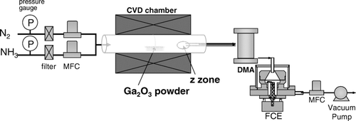
Various GaN nanostructures were synthesized using a typical atmospheric-pressure CVD reactor. As a precursor material, 2 g of Ga2O3 powder (Gallium (III) oxide ≥99.99%, Aldrich) was loaded in an alumina boat, which was placed at the center of a quartz-tube reactor. A Si substrate was placed 17 cm away from the center, which is indicated as a “z'’ zone in . The length of the quartz tube was 75 cm. The NH3 flow rate was varied as 400, 200, 50, and 0 standard cubic centimeters per minute (sccm) with nitrogen gas used as a carrier gas and the total flow rate (NH3+N2) was fixed at 600 sccm.
FIG. 2 Schematic for the DMA-FCE measurement system during atmospheric-pressure chemical vapor deposition.
In the synthesis of GaN using Ga2O3 powder and NH3 gas as Ga and N sources, respectively, NH3 starts to decompose at ∼500°C (Di Lello et al. Citation2002). It is expected that the generation of charged nanoparticles might be affected by the reactor temperature. To examine this effect, CVD was done at four reactor temperatures of 1100°C, 1000°C, 900°C, and 500°C with the deposition time of 30 min. After the alumina boat and the Si substrate were placed in the reactor, the reactor was heated to the preset temperature, which took 1 h. After deposition, the power was turned off and the reactor was cooled down to the room temperature.
In order to detect any charged nanoparticles that might be generated in the gas phase during the synthesis of GaN nanostructures, an in-situ differential mobility analyzer (Nano DMA, model 3085, TSI Inc., Shoreview, MN, USA) coupled with a Faraday cup electrometer (FCE) was installed to the atmospheric-pressure CVD system. The schematic for the experimental setup is shown in . As shown in , the nitrogen carrier gas and the NH3 gas were directly fed into the quartz tube reactor, and this mixture gas passing through the hot center zone of the reactor was supplied to the DMA-FCE system (Shimada et al. Citation2000, Citation2005), which measures the size distribution of the nanoparticles generated in the reactor.
Differential mobility analyzer (DMA) (Knutson and Whitby Citation1975a,b; Intra and Tippayawong Citation2008) has been used to classify the size of particles in the gas phase by electrostatic classification according to the difference in the electrical mobility of the particles. The electric charges carried by individual particles classified through the DMA are detected on the Faraday-cup electrometer (FCE) as an electrical current (Shimada et al. Citation2000, Citation2005). Since DMA can classify only the charged particles, particles are usually charged by artificial charging. In this study, however, particles are spontaneously charged in the reactor and no artificial charging was done. The particle sampling for DMA was done near the substrate as shown in . The nanostructures deposited on the Si substrate were observed by field-emission scanning electron microscopy (FESEM, JEOL JSM-7500F).
3. RESULTS AND DISCUSSION
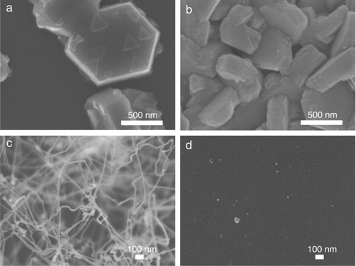
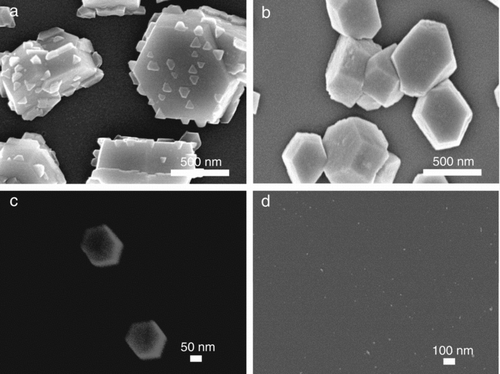
Since it was reported that GaN nanostructures were affected by the NH3 flow rate in the CVD process (Cai et al. Citation2006; Djurišić et al. Citation2008), the effect of the NH3 flow rate was examined with respect to the morphology of GaN nanostructure and the size distribution of charged nanoparticles. For this, the NH3 flow rate was made to vary from 400 to 0 sccm, with the total flow rate of 600 sccm fixed at the reactor temperature of 1100°C. The resultant GaN nanostructures are shown in . At the NH3 flow rates of 400 and 200 sccm, the hexagonal crystals were synthesized as shown in and , respectively. This hexagon shape has been already reported as a typical GaN crystal (Grzegory et al. Citation1995; Li et al. Citation1996). The deposition was nonuniform on the Si substrate; although the amount of GaN in appeared smaller than that in , the overall amount in the sample in was larger than that in .
FIG. 3 FESEM images of GaN nanostructures deposited at the flow rate of (a) 400 sccm, (b) 200 sccm, (c) 50 sccm, and (d) 0 sccm of the ammonia at a reactor temperature of 1100°C.
Energy dispersive spectroscopy (EDS, Horiba X-Max) of GaN crystals shows the atomic composition ratio of C:N:O: Si:Ga = 6.86:19.69:40.71:1.16:31.59. Carbon might be due to contamination during SEM observation and silicon might come from the substrate. However, a very large amount of oxygen was detected reproducibly. The oxygen might be formed by oxidation and absorption in the air when the sample was taken outside as suggested by Wolter and Tang (Wolter et al. Citation1998; Tang et al. Citation2003). Although the EDS is not accurate especially in the analysis of light elements, it poses a possibility that the GaN crystals formed in the reactor might be deficient in nitrogen and the excess Ga is oxidized in the air after the process.
As the NH3 flow rate decreased from 400 to 200 sccm, the size of hexagonal nanostructures decreased from ∼1 μm to ∼560 nm. At the NH3 flow rate of 50 sccm (), however, the one-dimensional structure of nanowires was grown instead of hexagonal crystals. The diameter of these nanowires was in the range of 10–20 nm. The total amount of nanowires deposited at the NH3 flow rate of 50 sccm was much smaller than that of hexagonal crystals deposited at the flow rates of 400 and 200 sccm. At the NH3 flow rate of 0 sccm, deposition hardly occurred as shown in as expected.
The weight losses of Ga2O3 precursor powder after the CVD process at 1100°C were 0.214 g, 0.176 g, 0.056 g, and 0.005 g, respectively, for the NH3 flow rates of 400, 200, 50, and 0 sccm. After the CVD process, the surface color of the precursor (Ga2O3) was changed from white to yellow for the NH3 flow rates of 400, 200, and 50 sccm, indicating the formation of GaN. For the flow rate of 0 sccm, however, the color remained white.
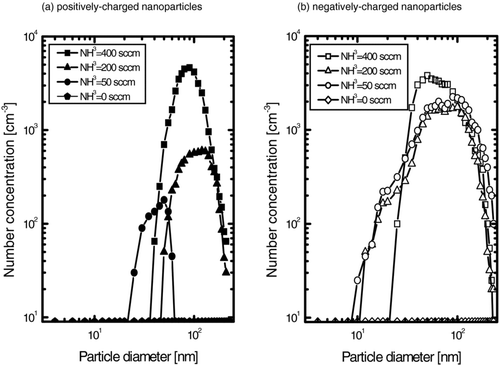
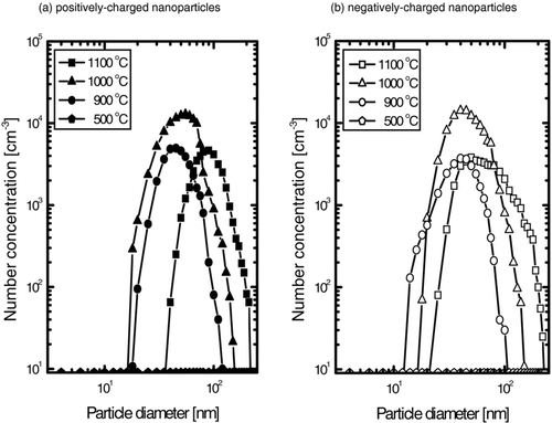
To confirm the generation of charged nanoparticles in the gas phase under conditions of GaN nanostructures growth shown in , in-situ measurements of charged nanoparticles were carried out using DMA-FCE system. shows the particle size distribution of charged GaN nanoparticles generated in the gas phase of the reactor at various NH3 flow rates. Both positively and negatively charged nanoparticles were generated. With decreasing flow rate of NH3, the number concentration and the size of both positively and negatively charged nanoparticles tended to decrease. However, in the absence of NH3 gas (0 sccm), charged nanoparticles were hardly detected as shown in , which is consistent with the negligible deposition of . This indicated that nucleation and charging of nanoparticles in the gas phase are enhanced with increasing NH3 flow rate due to enhancement of the formation of GaN. The NH3 flow rate affects the deposition behavior of GaN nanostructures, the amount of Ga2O3 precursor powder remaining after CVD, and the generation behavior of charged nanoparticles. For example, at the flow rate of 400 sccm, the size of GaN hexagonal crystals is largest (); the mass decrease of the precursor powder after CVD and the increase in the amount of generated charged nanoparticles () are also largest. At the flow rate of 0 sccm, however, the deposition of GaN was negligible in accordance with the negligible mass decrease of Ga2O3 powder and the negligible generation of charged nanoparticles.
FIG. 4 The size distribution of (a) positively and (b) negatively charged GaN nanoparticles with various NH3 flow rates at a reactor temperature of 1100°C.
The results show that whenever there was GaN growth, charged nanoparticles were generated. This aspect seems to be general because the charged nanoparticles were generated without exception under the growth condition of diamond (Hwang Citation1999; Jeon et al. Citation2000; Ahn et al. Citation2002), silicon film (Cheong et al. Citation1999; Lee et al. Citation2008; Kim et al. Citation2010b), ZnO nanowires (Kim et al. Citation2009a), CNTs (Lee and Hwang Citation2008; Kim et al. Citation2009b), and silicon nanowires (Kim et al. Citation2010a).
shows the FESEM images of GaN nanostructures synthesized at different reactor temperatures at the NH3 flow rate of 400 sccm. The size of hexagonal crystals decreased from ∼1 μm to ∼180 nm as the reactor temperature decreased from 1100°C to 900°C. At the reactor temperature of 500°C, GaN nanostructures were hardly synthesized as shown in , which might be attributed to the low decomposition rate of NH3 gas at 500°C (Di Lello et al. Citation2002).
FIG. 5 FESEM images of GaN nanostructures deposited at (a) 1100°C, (b) 1000°C, (c) 900°C, and (d) 500°C at a NH3 flow rate of 400 sccm.
shows the particle size distributions of positively and negatively charged GaN nanoparticles generated at various reactor temperatures under the processing conditions of the specimens in . In both and , the peak positions of the particle size decreased with decreasing reactor temperature. However, the particle number concentration shows different behavior, being largest at the reactor temperature of 1000°C. And the number concentrations of both positively and negatively charged nanoparticles were similar between 900°C and 1100°C. At the reactor temperature of 500°C, however, the GaN charged nanoparticles were hardly detected, which is consistent with the negligible deposition of .
FIG. 6 The size distribution of (a) positively and (b) negatively charged GaN nanoparticles with various reactor temperatures at a NH3 flow rate of 400 sccm.
It should be noted that the larger number concentration at 1000°C than at 1100°C does not necessarily mean that the total amount of charged particles generated at 1000°C is larger than that at 1100°C because the volume of the particle is proportional to the cube of the size. The weight losses were 0.214, 0.183, 0.069, and 0.000 g, respectively, for the reactor temperature of 1100°C, 1000°C, 900°C, and 500°C. After the CVD process, the surface color of the precursor (Ga2O3) was changed from white to yellow for the reactor temperatures of 1100°C, 1000°C, and 900°C with the color becoming lighter with decreasing temperature. For the reaction temperature of 500°C, however, the color remained white.
After deposition, the reactor wall was also coated in a yellowish color similar to the surface color on the substrate. This yellowish color on the quartz tube started to appear from the location of the crucible containing the source materials of Ga2O3 to the end of the tube although the color was not uniform along the tube. The color on the upper side of the reactor wall was thicker than that on the lower side, implying that the amount of deposition was larger on the upper side. The higher flow rate of NH3 and the higher reactor temperature made the color thicker on the reactor wall, implying that they increased the deposition rate.
In this study, one noticeable thing is that one-dimensional nanostructures were grown without catalysts as shown in , unlike the other reports which prepared nanowires by the catalyst-assisted growth (Zhou et al. Citation2005; Cai et al. Citation2006; Liu et al. Citation2006). In relation with such one-dimensional growth, Kim et al. (Citation2010a) reported that the structure of silicon deposited by atmospheric-pressure CVD was changed from films to nanowires when the size of charged silicon nanoparticles decreased. Si nanowires did not grow in the absence of smaller charged nanoparticles.
Kim et al.'s (Citation2010a) results are consistent with the experimental result of this study in which the growth of the one-dimensional nanowires occurs only when the smaller sized charged nanostructures are detected ( and ). From the results of various NH3 flow rates, only the 50 sccm of NH3 flow rate produced one-dimensional nanostructures as shown in . Hence, the one-dimensional growth of nanowires appears to be related with the smaller size and the lower number concentrations of charged nanoparticles generated at the flow rate of 50 sccm as shown in . However, the detailed correlation between the morphology of the GaN nanostructures and the size distribution of charged nanoparticles need to be studied further.
For the one-dimensional growth of diverse materials, the supersaturation ratio of condensing species is a prime consideration (Sears Citation1955; Campbell Citation1970; Xia et al. Citation2003). According to the previous study, a key factor of the microstructure evolution is the supersaturation ratio of condensing species, which is affected by the growth conditions such as the growth temperature and the flux of source materials. The supersaturation ratio determines the principal growth forms such as one-dimensional nanowires or whiskers, bulk crystal, and powders. A low supersaturation ratio produced the one-dimensional growth, whereas a medium or high supersaturation ratio produced bulk crystal or powders. Therefore, the supersaturation ratio might be one of candidates to explain the results of this article.
If the thermodynamic scheme of the supersaturation ratio for deposition of a compound in the CVD process (Hwang and Yoon Citation1994) is applied to GaN, the supersaturation ratio α is expressed as
The low supersaturation ratio mentioned in the previous study would produce a small amount of depositing flux, which would correspond to the small size and the small number concentration of charged nanoparticles generated in the gas phase of the CVD reactor. The previous experimental observation that the low supersaturation ratio produced one-dimensional structures are consistent with the present result of the nanowire synthesis shown in , where the small size and the small number concentration of charged GaN nanoparticles were generated as shown in .
and clearly show that charged nanoparticles are generated under typical processing conditions for GaN nanostructures. The actual number of concentrations in the CVD reactor would be higher than those shown in and , considering the loss of charged nanoparticles on the way up to the particle detection point. Although, further theoretical and experimental studies are needed to understand the charging mechanism, the possible mechanism for the formation of charged nanoparticles is that nucleation takes place first in the gas phase, and the neutral nuclei subsequently undergo surface ionization on any surface such as the quartz tube of the reactor (Hwang and Kim Citation2004).
The negative and positive surface ionization are described by the following Saha-Langmuir equations (Langmuir and Kingdon Citation1925; Brown Citation1995), respectively,
For the surface ionization of nanoparticles, EA and IP for nanoparticles should be used. Both EA and IP of nanoparticles, which contain so many atoms or molecules, are practically the work function of the bulk (Seidl et al. Citation1991). The work functions of SiO2 and quartz were reported, respectively, to be 4.4 eV (Lindmayer Citation1965) and 1.2 eV (Pagonis et al. Citation2009). 1.2 eV should be used for the work function of the quartz reactor tube. The work function of GaN was reported to vary widely in the range of 2.63–9.13 eV with its crystallographic faces (Tsai et al. Citation2002). The EA and IP of atoms or molecules are, respectively, much smaller and larger than those of nanoparticles. Therefore, charging of nanoparticles is much easier than that of atoms or molecules.
This means that the activation barrier for the surface ionization of nanoparticles, which is given by (WF–EA) and (IP–WF) in the above equations, would be much smaller than that for chemionization. Therefore, the surface ionization of nanoparticles would be a dominant mechanism for charging. The low activation energy for the surface ionization of nanoparticles might explain the low temperature charging in the CVD reactor. It should be noted that the contact charging experienced in daily life is a kind of the surface ionization between the macro objects.
The relative amount of positively and negatively charged nanoparticles varies sensitively with the location, the tube material, the temperature, and the processing conditions. The unbalanced amount of positively and negatively charged particles, which is frequently observed by DMA measurements, is difficult to explain. No conclusion could be drawn for the general tendency in the dominant polarity of charging yet.
Although this study shows that charged nanoparticles are generated under typical conditions for GaN nanostructures synthesis, their role in the growth of GaN nanostructures is not known. It is not yet certain whether the charged nanoparticles are mainly involved, partly involved, or hardly involved in the growth of GaN nanostructures. However, the experiments herein show that under conditions where charged nanoparticles were not generated, GaN nanostructures did not grow. This result clearly shows that the chemical reaction to produce GaN from Ga and N sources takes place not only on the surface but also extensively in the gas phase.
Considering the number density of charged GaN gas phase nuclei, their surface area is much larger than that of the reactor or substrate surface. Since the surface reaction is proportional to the surface area, the surface reaction to produce GaN from Ga and N sources would occur more dominantly on the surface of changed nanoparticles than on the reactor or substrate surface. Therefore, under the condition where extensive gas phase nucleation occurs, the surface reaction to produce GaN would occur mostly on the surface of gas phase nuclei. If it is assumed that the gas phase nuclei have no barrier in their collisions onto the substrate surface and contribute to film growth, their flux would be much more dominant than the flux contributed by the surface reaction on the substrate. Since these arguments pose the possibility that the charged gas phase nuclei might contribute significantly to growth of films or nanostructures, more systematic work is required to clarify the role of charged nanoparticles in deposition.
Even though the data for neutral particles are not shown here, an appreciable amount of them are expected to exist in the reactor. We tried to measure the percentage of neutral nanoparticles in other systems but the number concentration of generated nanoparticles was above the detection limit of our condensation particle counter (CPC, model 3025A, TSI lnc., Shoreview, MN, USA). Neutral nanoparticles, which have no electrostatic interaction, have no force attracting them to any surface in the reactor whereas charged nanoparticles have an appreciable attraction image force to the surface. In the presence of gas flow, the Saffman lift force would inhibit the particles from landing on the surface (Xu and Zhanhua 2009). Neutral particles would have difficulty in landing on the surface because there is no appreciable force for them to be attracted to the growing surface. Therefore, in the presence of gas flow, they are not expected to overcome the Saffman lift force; accordingly, their contribution to deposition would be much less than that of charged particles.
4. CONCLUSIONS
The generation of GaN charged nanoparticles was confirmed during the CVD process. The DMA-FCE measurements showed that both positively and negatively charged nanoparticles were generated in the gas phase. The process parameters of the reactor temperature and the NH3 flow rate affected not only the growth behavior of the GaN nanostructures but also the size distribution of charged nanoparticles. No GaN nanostructures were produced when these charged nanoparticles were not detected in the gas phase. Under the generation condition of charged nanoparticles smaller in size and number density, the size of GaN hexagonal crystals decreased. As the size and the number density decreased further, GaN nanowires began to grow without catalysts. The detailed correlation between the morphology of the GaN nanostructures and the size distribution of charged nanoparticles will be studied further.
Acknowledgments
The authors thank the reviewers for their helpful and constructive comments and are grateful for the financial support from the Brain Korea 21 program.
REFERENCES
- Adachi , M. , Okuyama , K. , Tohge , N. , Shimada , M. , Satoh , J. and Muroyama , M. 1992 . Gas-Phase Nucleation in an Atmospheric Pressure Chemical Vapor Deposition Process for SiO2 Films Using Tetraethylorthosilicate (TEOS) . Jap. J. Appl. Phys. , 31 : L1439 – L1422 .
- Adachi , M. , Okuyama , K. , Tohge , N. , Shimada , M. , Satoh , J. and Muroyama , M. 1993 . Particle Generation and Film Formation in an Atmospheric-Pressure Chemical Vapor Deposition Reactor Using the Tetraethylorthosilicate (TEOS)/He, TEOS/O2/He, and TEOS/O3/He Systems . Jap. J. Appl. Phys. , 32 : L748 – L751 .
- Adachi , M. , Okuyama , K. and Tohge , N. 1995 . Particle Generation and Film Formation in an Atmospheric-Pressure Chemical Vapour Deposition Process Using Tetraethylorthosilicate . J. Mater. Sci. , 30 : 932 – 937 .
- Adachi , M. , Okuyama , K. , Fujimoto , T. , Satoh , J. and Muroyama , M. 1996 . Morphology Control of Films Formed by Atmospheric-Pressure Chemical Vapor Deposition Using Tetraethylorthosilicate/Ozone System . Jap. J. Appl. Phys. , 35 : 4438 – 4443 .
- Ahn , H. S. , Park , H. M. , Kim , D. Y. and Hwang , N. M. 2002 . Observation of Carbon Clusters of a Few Nanometers in the Oxyacetylene Diamond CVD Process . J. Cryst. Growth , 234 : 399 – 403 .
- Amano , H. , Sawaki , N. , Akasaki , I. and Toyoda , Y. 1986 . Metalorganic Vapor Phase Epitaxial Growth of a High Quality GaN Film Using an AlN Buffer Layer . Appl. Phys. Lett. , 48 : 353 – 355 .
- Ambacher , O. 1998 . Growth and Applications of Group III-Nitrides . J. Phys. D: Appl. Phys. , 31 : 2653 – 2710 .
- Banholzer , W. 1992 . Understanding the Mechanism of CVD Diamond . Surf. Coat. Technol. , 53 : 1 – 12 .
- Brown , I. 1995 . Handbook of Ion Sources , New York : CRC Press .
- Cai , X. M. , Djurisic , A. B. and Xie , M. H. 2006 . GaN Nanowires: CVD Synthesis and Properties . Thin Solid Films , 515 : 984 – 989 .
- Campbell , W. B. 1970 . Growth of Whiskers by Vapor-Phase Reactions , New York, London, Sydney, Toronto : Wiley-Interscience .
- Cheong , W. S. , Hwang , N. M. and Yoon , D. Y. 1999 . Observation of Nanometer Silicon Clusters in the Hot-Filament CVD Process . J. Cryst. Growth , 204 : 52 – 61 .
- Choi , S. W. , Bachmann , K. J. and Lucovsky , G. 1993 . Growth Kinetics and Characterizations of Gallium Nitride Thin Films by Remote PECVD . J. Mater. Res. , 8 : 847 – 854 .
- Cvelbar , U. 2011 . Towards Large-Scale Plasma-Assisted Synthesis of Nanowires . J. Phys. D: Appl. Phys. , 44 : 174014
- Di Lello , B. C. , Moura , F. J. and Solózano , I. G. 2002 . Synthesis and Characterization of GaN Using Gas-Solid Reactions . Mater. Sci. Eng. B , 93 : 219 – 223 .
- Djurišić , A. B. , Cai , X. M. and Xie , M. H. 2008 . III-Nitride Nanomaterials: Growth and Properties , London : Imperial College Press .
- Grzegory , I. , Jun , J. , Bockowski , M. , Krukowski , S. T. , Wróblewski , M. Lucznik , B. 1995 . III-V Nitrides-Thermodynamics and Crystal Growth at High N2 Pressure . J. Phys. Chem. Solids , 56 : 639 – 647 .
- Han , W. , Fan , S. , Li , Q. and Hu , Y. 1997 . Synthesis of Gallium Nitride Nanorods through a Carbon Nanotube-Confined Reaction . Science , 277 : 1287 – 1289 .
- Hahn , J. H. , Hwang , N. M. and Yoon , D. Y. 1996 . Formation of Soot or Diamond on the Iron Substrate in the Chemical Vapour Deposition Process of Diamond . J. Mater. Sci. Lett. , 15 : 1240 – 1242 .
- Hirth , J. P. and Pound , G. M. 1963 . Condensation and Evaporation , Oxford : Pergamon Press .
- Hudgins , J. L. , Simin , G. S. , Santi , E. and Khan , M. A. 2003 . An Assessment of Wide Bandgap Semiconductors for Power Devices . IEEE Trans. Power Electron. , 18 : 907 – 914 .
- Hwang , N. M. and Yoon , D. Y. 1994 . Thermodynamic Approach to the Chemical Vapor Deposition Process . J. Cryst. Growth , 143 : 103 – 109 .
- Hwang , N. M. , Hahn , J. H. and Yoon , D. Y. 1996 . Charged Cluster Model in the Low Pressure Synthesis of Diamond . J. Cryst. Growth , 162 : 55 – 68 .
- Hwang , N. M. and Yoon , D. Y. 1996 . Thermodynamic Approach to the Paradox of Diamond Formation with Simultaneous Graphite Etching in the Low Pressure Synthesis of Diamond . J. Cryst. Growth , 160 : 98 – 103 .
- Hwang , N. M. 1999 . Evidence of Nanometer-Sized Charged Carbon Clusters in the Gas Phase of the Diamond Chemical Vapor Deposition (CVD) Process . J. Cryst. Growth , 204 : 85 – 90 .
- Hwang , N. M. and Kim , D. Y. 2004 . Charged Clusters in Thin Film Growth . Int. Mater. Rev. , 49 : 171 – 190 .
- Hwang , N. M. and Lee , D. K. 2010 . Charged Nanoparticles in Thin Film and Nanostructure Growth by Chemical Vapour Deposition . J. Phys. D: Appl. Phys. , 43 : 483001
- Intra , P. and Tippayawong , N. 2008 . An Overview of Differential Mobility Analyzers for Size Classification of Nanometer-Sized Aerosol Particles . Songklanakarin J. Sci. Technol. , 30 : 243 – 256 .
- Jeon , J. D. , Park , C. J. , Kim , D. Y. and Hwang , N. M. 2000 . Experimental Confirmation of Charged Carbon Clusters in the Hot Filament Diamond Reactor . J. Cryst. Growth , 213 : 79 – 82 .
- Jeon , I. D. , Gueroudji , L. , Kim , D. Y. and Hwang , N. M. 2001a . Temperature Dependence of the Deposition Behavior of Yttria-Stabilized Zirconia CVD Films: Approach by Charged Cluster Model . J. Korean Ceram. Soc. , 38 : 218 – 224 .
- Jeon , I. D. , Park , C. J. , Kim , D. Y. and Hwang , N. M. 2001b . Effect of Methane Concentration on Size of Charged Clusters in the Hot Filament Diamond CVD Process . J. Cryst. Growth , 223 : 6 – 14 .
- Kim , C. S. , Chung , Y. B. , Youn , W. K. and Hwang , N. M. 2009a . Generation of Charged Nanoparticles during Synthesis of ZnO Nanowires by Carbothermal Reduction . Aerosol Sci. Technol. , 43 : 120 – 125 .
- Kim , C. S. , Chung , Y. B. , Youn , W. K. and Hwang , N. M. 2009b . Generation of Charged Nanoparticles during the Synthesis of Carbon Nanotubes by Chemical Vapor Deposition . Carbon , 47 : 2511 – 2518 .
- Kim , C. S. , Youn , W. K. and Hwang , N. M. 2010b . Generation of Charged Nanoparticles and Their Deposition during the Synthesis of Silicon Thin Films by Chemical Vapor Deposition . J. Appl. Phys. , 108 : 014313
- Kim , C. S. , Kwak , I. J. , Choi , K. J. , Park , J. G. and Hwang , N. M. 2010a . Generation of Charged Nanoparticles during the Synthesis of Silicon Nanowires by Chemical Vapor Deposition . J. Phys. Chem. C , 114 : 3390 – 3395 .
- Kim , J. Y. , Kim , D. Y. and Hwang , N. M. 2006 . Spontaneous Generation of Negatively Charged Clusters and Their Deposition as Crystalline Films during Hot-Wire Silicon Chemical Vapor Deposition . Pure Appl. Chem. , 78 : 1715 – 1722 .
- Knutson , E. O. and Whitby , K. T. 1975a . Aerosol Classification by Electric Mobility: Apparatus, Theory, and Applications . J. Aerosol Sci. , 6 : 443 – 451 .
- Knutson , E. O. and Whitby , K. T. 1975b . Accurate Measurement of Aerosol Electric Mobility Moments . J. Aerosol Sci. , 6 : 453 – 460 .
- Langmuir , I. and Kingdon , K. H. 1925 . Thermionic Effects Caused by Vapours of Alkali Metals . Proc. R. Soc. London, Ser. A , 107 : 61 – 79 .
- Lee , B. S. , Barnes , M. C. , Kim , D. Y. and Hwang , N. M. 2002a . Spontaneous Generation of Charged Clusters of a Few Nanometers during Thermal Evaporation of Copper . J. Cryst. Growth , 234 : 599 – 602 .
- Lee , J. I. and Hwang , N. M. 2008 . Generation of Negative-Charge Carriers in the Gas Phase and Their Contribution to the Growth of Carbon Nanotubes during Hot-Filament Chemical Vapor Deposition . Carbon , 46 : 1588 – 1592 .
- Lee , S. C. , Hwang , N. M. , Yu , B. D. and Kim , D. Y. 2001 . Molecular Dynamics Simulation on the Deposition Behavior of Nanometer-Sized Au Clusters on a Au (001) Surface . J. Cryst. Growth , 223 : 311 – 320 .
- Lee , S. C. , Yu , B. D. , Kim , D. Y. and Hwang , N. M. 2002b . Effects of Cluster Size and Substrate Temperature on the Homoepitaxial Deposition of Au Clusters . J. Cryst. Growth , 242 : 463 – 470 .
- Lee , S. S. , Ko , M. S. , Kim , C. S. and Hwang , N. M. 2008 . Gas Phase Nucleation of Crystalline Silicon and Their Role in Low-Temperature Deposition of Microcrystalline Films during Hot-Wire Chemical Vapor Deposition . J. Cryst. Growth , 310 : 3659 – 3662 .
- Li , H. D. , Yang , H. B. , Yu , S. , Zou , G. T. , Li , Y. D. Liu , S. Y. 1996 . Synthesis of Ultrafine Gallium Nitride Powder by the Direct Current Arc Plasma Method . Appl. Phys. Lett. , 69 : 1285 – 1287 .
- Lindmayer , J. 1965 . Heterojunction Properties of the Oxidised Semiconductor . Solid State Electron. , 8 : 523 – 528 .
- Liu , B. , Bando , Y. , Tang , C. , Shen , G. , Golberg , D. and Xu , F. 2006 . Wurtzite-Type Faceted Single-Crystalline GaN Nanotubes . Appl. Phys. Lett. , 88 : 093120 – 093123 .
- Mishra , U. K. , Parikh , P. and Yi-Feng , W. 2002 . AlGaN/GaN HEMTs—an Overview of Device Operation and Applications . Proc. IEEE , 90 : 1022 – 1031 .
- Neudeck , P. G. , Okojie , R. S. and Liang-Yu , C. 2002 . High-Temperature Electronics—a Role for Wide Bandgap Semiconductors? . Proc. IEEE , 90 : 1065 – 1076 .
- Nunomura , S. , Koga , K. , Shiratani , M. , Watanabe , Y. , Morisada , Y. Matsuki , N. 2005 . Fabrication of Nanoparticle Composite Porous Films Having Ultralow Dielectric Constant . Jap. J. Appl. Phys. , 44 : L1509 – L1511 .
- Orton , J. W. and Foxon , C. T. 1998 . Group III Nitride Semiconductors for Short Wavelength Light-Emitting Devices . Rep. Prog. Phys. , 61 : 1 – 75 .
- Ostrikov , K. 2005 . Colloquium: Reactive Plasmas as a Versatile Nanofabrication Tool . Rev. Mod. Phys. , 77 : 489 – 510 .
- Ostrikov , K. and Murphy , A. B. 2007 . Plasma-Aided Nanofabrication: Where is the Cutting Edge? . J. Phys. D: Appl. Phys. , 40 : 2223 – 2241 .
- Ostrikov , K. , Levchenko , I. , Cvelbar , U. , Sunkara , M. and Mozetic , M. 2010 . From Nucleation to Nanowires: A Single-Step Process in Reactive Plasmas . Nanoscale , 2 : 2012 – 2027 .
- Pagonis , V. , Ankjærgaard , C. , Murray , A. S. and Chen , R. 2009 . Optically Stimulated Exoelectron Emission Processes in Quartz: Comparison of Experiment and Theory . J. Lumin. , 129 : 1003 – 1009 .
- Peng , H. Y. , Zhou , X. T. , Wang , N. , Zheng , Y. F. , Liao , L. S. , Shi , W. S. , Lee , C. S. and Lee , S. T. 2000 . Bulk-Quantity GaN Nanowires Synthesized from Hot Filament Chemical Vapor Deposition . Chem. Phys. Lett. , 327 : 263 – 270 .
- Piekarczyk , W. 1998 . How and Why CVD Diamond is Formed: A Solution of the Thermodynamic Paradox . J. Mater. Sci. , 33 : 3443 – 3453 .
- Roca i Cabarrocas , P. 2000 . Plasma Enhanced Chemical Vapor Deposition of Amorphous, Polymorphous and Microcrystalline Silicon Films . J. Non-Cryst. Solids , 266–269 : 31 – 37 .
- Roca i Cabarrocas , P. 2002 . Plasma Enhanced Chemical Vapor Deposition of Silicon Thin Films for Large Area Electronics . Curr. Opin. Solid State Mater. Sci. , 6 : 439 – 444 .
- Sears , G. W. 1955 . A Mechanism of Whisker Growth . Acta Metall. , 3 : 367 – 369 .
- Seidl , M. , Meiwes-Broer , K. H. and Brack , M. 1991 . Finite-Size Effects in Ionization Potentials and Electron Affinities of Metal Clusters . J. Chem. Phys. , 95 : 1295 – 1303 .
- Shimada , M. , Iskandar , F. and Okuyama , K. 2000 . Development of DMA-Faraday Cup Electrometer System for Measurement of Submicron Aerosol Particles . AIP Conf. Proc. , 534 : 773 – 776 .
- Shimada , M. , Lee , H. M. , Kim , C. S. , Koyama , H. , Myojo , T. and Okuyama , K. 2005 . Development of an LDMA-FCE System for the Measurement of Submicron Aerosol Particles . J. Chem. Eng. Jpn. , 38 : 34 – 44 .
- Takamura , Y. , Hayasaki , K. , Terashima , K. and Yoshida , T. 1997 . Cluster Size Measurement Using Microtrench in a Thermal Plasma Flash Evaporation Process . J. Vac. Sci. Technol., B , 15 : 558 – 565 .
- Tang , C. , Bando , Y. and Liu , Z. 2003 . Thermal Oxidation of Gallium Nitride Nanowires . Appl. Phys. Lett. , 83 : 3177 – 3179 .
- Tsai , M. H. , Sankey , O. F. , Schmidt , K. E. and Tsong , I. S. T. 2002 . Electronic Structures of Polar and Nonpolar GaN Surfaces . Mater. Sci. Eng. B , 88 : 40 – 46 .
- Vladimirov , S. V. and Ostrikov , K. 2004 . Dynamic Self-Organization Phenomena in Complex Ionized Gas Systems: New Paradigms and Technological Aspects . Phys. Rep. , 393 : 175 – 380 .
- Wolter , S. D. , Mohney , S. E. , Venugopalan , H. , Wickenden , A. E. and Koleske , D. D. 1998 . Kinetic Study of the Oxidation of Gallium Nitride in Dry Air . J. Electrochem. Soc. , 145 : 629 – 632 .
- Xia , Y. , Yang , P. , Sun , Y. , Wu , Y. , Mayers , B. Gates , B. 2003 . One-Dimensional Nanostructures: Synthesis, Characterization, and Applications . Adv. Mater. , 15 : 353 – 389 .
- Xu , Z. and Zhanhua , S. L. 2009 . The Influence of Saffman Lift Force on Nanoparticle Concentration Distribution Near a Wall . Appl. Phys. Lett. , 95 : 124105
- Yarbrough , W. A. 1992 . Vapor-Phase-Deposited Diamond—Problems and Potential . J. Am. Ceram. Soc. , 75 : 3179 – 3200 .
- Yasui , K. , Morimoto , K. and Akahane , T. 2003 . Growth of GaN Films on NitridedGaAs Substrates Using Hot-Wire CVD . Thin Solid Films , 430 : 174 – 177 .
- Zhou , X. T. , Sham , T. K. , Shan , Y. Y. , Duan , X. F. , Lee , S. T. and Rosenberg , R. A. 2005 . One-Dimensional Zigzag Gallium Nitride Nanostructures . J. Appl. Phys. , 97 : 1 – 6 .