
 ?Mathematical formulae have been encoded as MathML and are displayed in this HTML version using MathJax in order to improve their display. Uncheck the box to turn MathJax off. This feature requires Javascript. Click on a formula to zoom.
Abstract
The problem of the efficiency of energy transfer from a capacitive energy storage device to the region of nanoparticle synthesis in a spark discharge has been considered. Using the method for measuring pulsed voltages at short gas-discharge gaps developed by the authors, the time dependence of the voltage across the active resistance of the gaps was studied for copper and titanium electrodes in different discharge regimes. For the first time, stepwise changes were observed in the time dependence of the voltage at the moments of changing the current direction. The conclusion was made about the predominant release of electrical energy in the near-electrode regions of the discharge gap, where nanoparticle synthesis occurs. For a spark discharge, the voltage across the active resistance of the interelectrode gap weakly depends on the amplitude of the flowing current and, for metal electrodes, is of the order of several tens of volts. A formula is proposed for determining the energy transferred to the discharge gap. The efficiency of energy transfer to the discharge gaps increases with increasing the quality of the discharge circuit with the use of several series-connected interelectrode gaps (in our case, from 30 to 60%), with a decrease in the capacitance or initial voltage at the capacitor.
Copyright © 2019 American Association for Aerosol Research
Introduction
The synthesis of nanoparticles in a spark discharge is a promising method for producing nanoparticles of novel phases as well as composites with small sizes of 1–20 nm (CitationTabrizi et al. 2009; Maisser et al. Citation2015) from conductive materials: metals and doped semiconductors (Vons et al. Citation2011; Mylnikov et al. Citation2018). This aerosol method does not involve solvents, surfactants, or precursors, as well as any sources of contaminants and pollution. One powerful application of the spark is synthesizing mixtures of metallic particles using either alloys or sintered mixed powders as electrodes, or two electrodes of different composition (Evans, Harrison, and Ayres Citation2003; Lafont et al. Citation2009; Byeon, Park, and Hwang Citation2008). The possibility of nanoscale production of arbitrary mixtures of materials is attractive with regard to their applications in catalysis, hydrogen storage, as electrodes for lithium-ion batteries, etc. A variety of nanoparticles produced by the spark discharge are applied in electronics for improving oxide–semiconductor memory devices (Chakraborty et al. Citation2011), in medicine for drug delivery (Rai et al. 2016), in aerosol synthesis of single-walled carbon nanotubes (Krasnikov et al. Citation2019), and in aerosol printing of microstructures (Efimov et al. Citation2018; Ivanov et al. Citation2018; Arsenov, Efimov, and Ivanov Citation2018). To date, much attention has been paid to the study of various regimes of the nanoparticle synthesis (Pfeiffer, Feng, and Schmidt-Ott Citation2014), various designs of spark discharge generators (SDG) (Noh et al. Citation2017; Han et al. Citation2012; Ivanov et al. Citation2016), and the development of the methods for synthesizing non-oxidized nanoparticles (Hallberg et al. Citation2018). Despite the fact that the performance of spark-discharge nanoparticle generators improves every year, the issue of high energy consumption per gram of the synthesized particles remains relevant.
According to the researchers' estimates, only a small part (∼0.2%) of the energy input in the discharge circuit is converted into thermal energy of the material evaporated from the electrode surface (Feng, Biskos, and Schmidt-Ott Citation2015). The entry into industrial-scale production of nanoparticles (Slotte and Zevenhoven Citation2017) requires a reduction in losses in energy transmission from the discharge circuit energy storage device directly to the region of the nanoparticle synthesis.
The nanoparticle synthesis occurs in the interelectrode gap. In this regard, it is of interest to investigate the dependence of the nanoparticle synthesis not on the initial energy of the energy storage device, as many researchers did, but on the energy released in the gap between the electrodes, which can be significantly smaller due to losses in the discharge circuit elements. It is important to analyze in detail the use of the capacitive energy storage device since the majority of researchers use high-frequency capacitor banks as the energy storage device in the pulse-discharge circuit.
The control of the energy transferred to the interelectrode gap is possible through direct measurements of the pulsed current in the gap and the active voltage across it. Measurements of pulsed current in the discharge circuit by pulsed measuring transformers are well established, while measurements of the active voltage across short spark gaps are a challenging task. Pulsed voltage measurements in SDGs are usually made using commercial high-voltage probes. Such measurements did not allow to observe the shape of the voltage pulse across the active resistance of the gap since, due to the high frequency of current oscillations (100–1000 kHz), the voltage component across the inductive sections of the measuring circuit is many times higher than the desired signal of the resistive component (Palomares et al. Citation2015).
Measurements of the energy transferred to the gap can be made by simultaneously measuring the pulse current I(τ) and the voltage Ugap(τ) across the gap and calculating the integral When using this technique, it is also required to avoid the appearance of closed loops in the measuring circuit, leading to large inductive interference. The method is also sensitive to high-frequency interference from the discharge circuit, and in order to achieve sufficient accuracy, it requires the organization of correct wiring and shielding of the current and voltage sensors as well as the measuring oscilloscope. Without the fulfillment of these conditions, the measurements cannot be considered reliable, although attempts at such measurements have been made (Zhong et al. Citation2015; Pai et al. Citation2013).
In this article, we use the developed method of measuring pulsed voltages at short discharge gaps for measuring voltages across the spark gaps. Based on the analysis of the detected regularities, we propose an algorithm for determining the energy transfer to such gaps.
Experimental methods
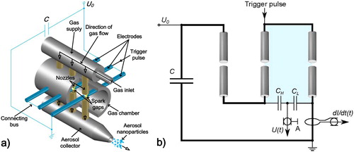
Experimental studies were performed using a three-gap SDG. presents a 3D model of a discharge chamber with a gas supply system, electrode assembly, and pulsed discharge circuit of the SDG, and shows an electrical diagram of the discharge circuit and probes for simultaneous measurements of pulsed voltages and currents. The high-current discharge circuit consists of a capacitive energy storage device and three pairs of electrodes connected in series. The high-voltage source allows repetitive charging of the capacitive energy storage device with a frequency of 0.5–10 Hz to a voltage of up to 6 kV. A low-inductance film-paper capacitor K75-48M (ELKOD, Russia) with a capacitance of 0.97 mF was used as the capacitive energy storage device. Cylindrical copper and titanium electrodes with a diameter of 10 mm, located in a cylindrical dielectric chamber, were used; the axes of the electrodes were perpendicular to the chamber axis. The interelectrode gaps in all pairs were set the same within 0.5–1.5 mm. The controlled breakdown of the gaps was initiated by a short (about 1 μs) high-voltage (20–30 kV) trigger pulse fed to the middle electrode, by analogy with the functioning of multigap gas-filled switches (Mesyats 2004). The energy of the trigger pulse was much less than the energy stored in the capacitive storage and did not have a significant effect on the energy release in the interelectrode gaps. The synthesis of nanoparticles was carried out in the atmosphere of purified air pumped through the discharge chamber by a compressor; the total flow was 80 lpm. During repetitive spark discharges in the interelectrode gaps, each pair of electrodes is purged with the gas flow directed perpendicular to the electrodes and chamber axis, which ensures the removal of the aerosol nanoparticles from the interelectrode gap. At the same time, intense purging ensures the electric strength restoration in the gap prior to the next discharge pulse. From the opposite side of the discharge chamber, an aerosol collector captures aerosol flows with nanoparticles, and the nanoparticles settle on the TEM grids in the collector for further examination by a JEM-2100 transmission electron microscope (JEOL).
Figure 1. (a) 3D model of a discharge chamber with a system of gas supply, an arrangement of electrodes and a pulsed discharge circuit of the SDG; (b) electrical scheme of the discharge circuit and simultaneous measurements of pulsed voltages and currents in SDG. CH and CL represent the capacitive voltage divider. The bold line is a high-current discharge circuit. The filled area marks a low-inductance bifilar loop.
To correlate the data of this work with the published results of scientific groups engaged in the research on nanoparticle production in a spark discharge, we provided in the a comparison of the parameters of the SDG employed with those given in recent publications (Guo et al. Citation2013; Helsper et al. Citation1993; Kohut et al. Citation2017; Palomares et al. Citation2015; CitationTabrizi et al. 2009; Wagner et al. Citation2016). The values of the energy storage capacitance C, its charging voltage U0, frequency of discharges f, gas flow per gap QN, stored energy per gap EN, average power per gap defined as the product EN f, and the types of electrode materials are presented. It is important to note that, for our installation, the values of QN, EN, and the average power per gap EN f are defined as the corresponding values for the entire SDG divided by the number of interelectrode gaps, N = 3. From , we can see that the range of energies stored per gap in our installation contains the upper value of the energies used previously by other scientific groups. In terms of the average power, the range of our installation lies in the middle of the ranges used by other groups due to the low repetition rate. The moderate values of the energy stored in the capacitor per one gap at a sufficiently large capacitance are due to the low gap breakdown voltage together with the distribution of energy over three gaps. Indeed, due to the triggered breakdown of three gaps connected in series, the discharge capacitor voltage (2–5 kV) is 2–3 times lower than in the case of self-breakdown of such discharge gaps. The highest gas flow per gap QN (compared with other research groups, see ) in our installation provides good cooling of electrodes.
Table 1. Parameters of the spark discharge generator employed in this study compared with those described in recent publications.
For measurements of the pulsed voltage across the interelectrode gap, we used the method we developed previously (Myl’nikov et al. Citation2016). The reliability of the measurements was achieved by elimination of electromagnetic interference in the measuring circuit, which was checked by control measurements. First, the shielding of the measuring circuit was carefully organized (Ott Citation1976; Schwab Citation1972). For this, the entire circuit, including the voltage and current sensors and the oscilloscope, was grounded only at one point coinciding with the grounding point of the high-current discharge circuit. Such grounding minimizes the number of closed loops causing electromagnetic interference. The measuring circuit with coaxial cables was placed inside additional shielding. These steps provided a means to make measurements with two sensors simultaneously, eliminating both the sensor crosstalk and the effect of interference from the high-current circuit. All pulse measurements were carried out using a Tektronix DPO4102B-L two-channel digital oscilloscope.
Second, pulsed voltage measurements were carried out with a low-inductance section of the discharge circuit of the three-gap SDG in the form of a bifilar loop with inductance L (highlighted in ) including two interelectrode gaps, which significantly reduced the voltage component associated with the voltage drop across the inductive resistance of the considered circuit section. With the help of a specially manufactured high-frequency voltage sensor (capacitive voltage divider) and a current sensor (measuring transformer), the dependences of these parameters on time were measured. Then, the voltage drop across the active resistance of the gap was calculated using the formula
(1)
(1)
Since the discharge circuit is symmetric with respect to the change of the current direction, the shape of the dependence Ugap(t) must be symmetric about the zero voltage value. The value of the loop inductance L to be substituted in (1) is determined so that the stepwise voltage changes occur symmetrically with respect to the zero voltage value. The value of L was 155 ± 10 nH. The theoretical estimate of the inductance of this loop gave the same result.
The measured time dependences of the voltage across the interelectrode gaps and the derivative of the current show stepwise changes in the amplitude of the signals at the moment the current passes through zero, observed for the first time for such processes ( and ). In the insets of and at the upper right corner, there are sections of stepwise changes in the derivative of the current and voltage across the interelectrode gaps with magnifications of 5 and 7, respectively. The dependences of the voltage across the active resistance of the interelectrode gap calculated from the measured data are an alternating function that can be represented as the sum of two functions: square wave with approximately constant amplitude Udrop(t) and damping function UI(t), with its amplitude decreasing with decreasing the current amplitude ().
Figure 2. Time dependencies of (a) derivative of current from current sensor, (b) voltage from voltage divider, (c) current in circuit, and (d) half of voltage on active resistance of the studied section of circuit with two interelectrode gaps (i.e., voltage for 1 gap). The initial voltage on the capacitive energy storage device is 2.5 kV, the distance between the electrodes is 0.5 mm, and the electrodes are made of copper.
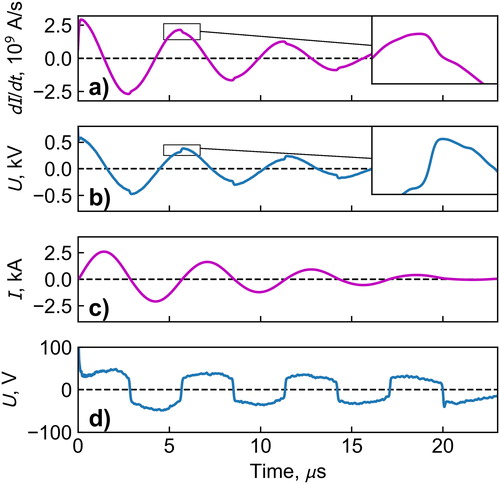
Figure 3. Calculation of Udrop, UI and IA for each half-period of oscillations from measurements of the dependence of the voltage on the active resistance of the gap and the current in the discharge circuit on time.
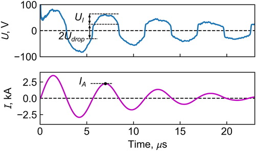
Using the waveforms of voltage and current versus time, averaged over 10 measurements, we measured the values of Udrop, i.e., the height of the stepwise changes, UI, i.e., the height of the “caps”, and current amplitude IA of current I(t) at the corresponding time for each half-period of oscillations ().
The source of trigger pulses allowed to initiate the breakdown of three series-connected interelectrode gaps at a fixed voltage at the capacitive energy storage device in a wide range of values of the interelectrode distances. shows the results of such measurements of pulsed voltages at the interelectrode gaps with the values of the gaps between titanium electrodes in the range from 0.5 to 1.5 mm and the calculated dependencies of voltages Udrop and UI across the gap on the current amplitude IA. The dependences were then approximated by linear functions
(2)
(2)
using the least-squares method.
Figure 4. The dependence of the voltage on the active resistance of the interelectrode gaps on the time at three different values of the distance between the titanium electrodes (left), the initial voltage on the capacitive energy storage device was 5 kV in all cases. Calculation of the dependence of Udrop and UI on the amplitude of the current IA (right). The slope coefficients AI, Adrop calculated by the least squares method are given.
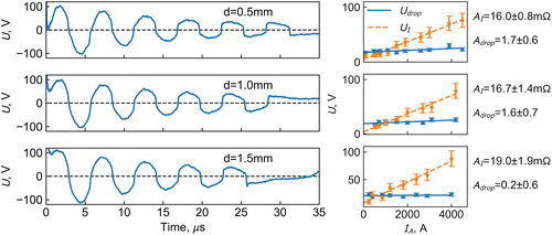
Comparing the results obtained for the interelectrode gaps with different distances between the electrodes, one can see that the amplitude of voltage Udrop almost does not depend on the amplitude of the discharge current and the spacing of the interelectrode gap and is in the range from 16.4 to 21.1 V for titanium.
The data obtained make it possible to relate the voltage amplitude Udrop to the electrode voltage drop (cathode and anode), which is known to be almost independent of the current and the distance between the electrodes in arc discharges.
Earlier in the work (Pfeiffer Citation2014), the experimentally confirmed fact that the spark behavior is essentially independent of the gap length has already been noted. Thanks to the use of triggered switching on of the discharge current in the SDG with one discharge gap, it was possible to measure the dynamics of the transfer of fixed-value capacitor energy to the discharge circuit by varying the gap spacing in the range of 0.5–2.2 mm. For all distances between the electrodes, the energy absorption in the discharge circuit was characterized by very close time dependencies. These data are in good agreement with our result, despite the fact that the values of the energy stored in the capacitors differ by a factor of about 115. This indicates a single mechanism of the spark discharge in a wide range of storage energy and discharge current values.
The dependence of UI on the current amplitude is a linear function that intersects the abscissa axis near the origin and behaves like an active voltage at a constant resistance (). The coefficient of proportionality between the voltage and current for the UI(IA) dependence does not depend on the distance between the electrodes, when it changes three times and is in the range of 17.3–19.0 mΩ, which indicates the insignificant contribution of the voltage drop across the plasma channel and gives a reason to assign the voltage component UI to the voltage drop across the active resistance of the regions of electrodes involved in the measuring circuit.
The values of the near-electrode component of the voltage drop Udrop and the component UI responsible for the voltage drop across the electrodes, depending on the current amplitude, were measured and compared for electrodes made from two materials: copper and titanium; the results are presented in .
Figure 5. Time dependence of the voltage across the active resistance of the interelectrode gaps for copper and titanium electrodes (left); the distance between the electrodes is 0.5 mm; the initial voltage at the capacitive energy storage device is 2.6 kV. Calculated dependencies of Udrop and UI on the current amplitude IA (right). The slopes AI, Adrop calculated by the least-squares method are given.
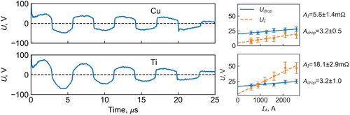
shows the values of the sum of the cathode and anode voltage drops for one gap at current values in the range of 0.6–2 kA. For metal electrodes, these values are close to those measured earlier for quasistationary discharges in short gaps: 16.5 V for copper and 14–17 V for other metals (Cu-W, Fe, W) in the current range from 10 to 20,000 A (Yokomizu et al. Citation1996), and 22–42 V for electrodes from Mg, W, Zn, Cd for pulsed discharges at current values from 200 to 600 A (Cundall and Craggs Citation1955).
Table 2. Sum of the cathode and anode voltage drops for one gap at current values in the range of 0.6–2 kA and calculated electrical resistance of one pair of electrodes.
The electrical resistance calculated from the component of the voltage drop across the electrodes UI for copper and titanium electrodes (5.5; 18.1 mΩ, respectively) turned out to be 4–5 mΩ higher than the theoretically calculated value at the oscillation frequency of the discharge current of 175 kHz (taking into account the skin effect). Probably, the difference arises due to unaccounted contact resistance and narrowing of the current channel at the boundary of the electrode and the spark channel.
The nanoparticles synthesized in the processes of the spark discharge were examined using a JEOL JEM2100 transmission electron microscope ( and ). The average sizes of the nanoparticles synthesized with electrodes from titanium and copper, obtained from size distribution histograms measured by TEM images, amount to 7.4 ± 0.2 and 7.6 ± 0.2 nm, respectively ( and ). The distribution of the numerical fraction of particles over diameters is described well by a logarithmic-normal distribution function. The nanoparticles were assembled into agglomerates. Diffraction patterns in the insets ( and ) show that the particles have a crystalline structure and consist of titanium and copper oxides. Both diffraction patterns reveal a ring structure and some intense single spots that are indicative of two phases with different nanoparticle sizes. The diffraction patterns were taken only for those nanoparticles that are represented in the images. It is important to note that we did not observe large micron-sized particles of micron sizes in this study. Therefore, it is logical to assume that the fractions of smaller nanoparticles are represented by concentric rings, by which, in the first case, they are identified as anatase TiO2 and in the second one—as copper oxide Cu2O. The groups of intense single spots in the diffraction patterns probably correspond to the largest crystalline nanoparticle or several nanoparticles, which, in the first case, can be rutile TiO2, and full copper oxide CuO in the second case.
Figure 6. TEM images of nanoparticles synthesized with electrodes from (a) titanium and (b) copper, with a voltage on the capacitive energy storage device 2.0 kV. The insets show an electron diffraction pattern. Size distribution histograms measured by TEM images approximated by a logarithmically normal function for nanoparticles synthesized with electrodes from (c) titanium and (d) copper.
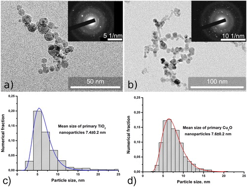
It should be noted that in the processes of nanoparticle synthesis in air, partial oxidation of the electrode surfaces took place. In the area of electrode erosion, their surfaces acquired a white tint in the case of titanium electrodes and a black tint in the case of copper electrodes. The nature of the electrode oxidation did not prevent the synthesis of oxide nanoparticles, which was stable over time.
To determine the mass production rate of the synthesis of nanoparticles, they were collected on a Thermovent HEPA filter, and the nanoparticle mass was measured by weighing the filter before and after the collection procedure. The maximum mass production rate for the three-gap SDG was 18 and 27 mg/h, and the corresponding energy consumption was of about 1.9 and 1.3 kWh/g for the synthesis of nanoparticles of titanium and copper oxides, respectively.
Thus, we found that the active voltage Udrop across the electrode gap depends on the electrode material and almost does not change with the current amplitude. It is this voltage that is responsible for the electrical energy input in the process of the nanoparticle synthesis.
Results and discussion
As shown by the measurements, not all the energy originally stored in the capacitive energy storage device is spent on the synthesis of nanoparticles. Only the part of the energy transferred to the near-electrode regions is involved in the synthesis. The rest of the energy is dissipated at the active resistance of the capacitive energy storage device, connecting busbars, contacts, and the electrodes themselves.
Let us calculate the time dependence for the fraction of energy delivered to the discharge gaps (energy efficiency) for the employed SDG by the following formula
(3)
(3)
where C is the capacitance of the energy storage device, U0 is the initial voltage across it, I(τ) is the current through the discharge gap, U(τ) is the voltage across the active resistance of the gap. Given that the active voltage on the interelectrode gap is approximately constant in amplitude and equal to Udrop, formula Equation(3)
(3)
(3) can be reduced to
(4)
(4)
shows the dependences η(t) calculated for the discharge circuits with one and three interelectrode gaps used in the study.
Figure 7. The fraction of energy η(t) transferred to the interelectrode gaps, calculated by the formula (4) for circuits with one and three gaps.
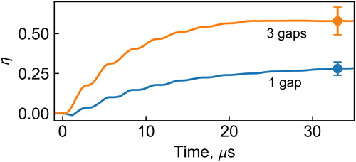
Thus, in the discharge circuit with one interelectrode gap, the fraction of energy transferred to the gap was only about 30%, the rest was dissipated as heat at parasitic resistances. Our case demonstrates that the capacitor ESR at the oscillation frequency of the discharge circuit was 70 mΩ. As we have shown, the resistance of the electrodes themselves can be tens of mΩ. It is especially important to take into account and minimize the length of electrodes when using electrodes made of doped semiconductors that have high resistance, for example, germanium electrodes (Mylnikov et al. Citation2018). It is required to use current-carrying busbars of sufficient perimeter in cross-section in order to minimize their active resistance, taking into account the skin effect. For example, we used a 2-cm wide copper busbar with a total busbar length of 0.7 m; its resistance was 17 mΩ at an oscillation frequency of 150 kHz.
The investigation of the voltage across the active resistance of the circuit by varying the length of the gap showed that, inside the discharge gap, the main voltage drop occurs in the near-electrode regions. This is consistent with the well-known concepts of the pulsed gas discharge. In the operation mode under study, the duration of the leader-streamer stage of formation of a plasma channel, which takes several nanoseconds, is negligible compared with the time the discharge exists: a few microseconds. Therefore, in the regime under study, the plasma has the same state as in the arc discharge where the voltage drop along the discharge channel itself is small and mainly occurs in the near-electrode regions (Bazelyan and Raizer Citation1997).
Based on the results obtained, we propose the following formula for estimating the fraction of energy η delivered directly to the synthesis region. We define it as the energy transferred to the near-electrode regions with respect to the total energy of the capacitive storage:
(5)
(5)
where qtot is the total charge flowing through the interelectrode gap during one discharge pulse.
In the case of a capacitive energy storage device, the full charge is as follows
(6)
(6)
where Q is the quality factor of the discharge circuit.
The fraction of energy delivered at discharge intervals can be represented as
(7)
(7)
where N is the number of the series-connected interelectrode gaps, Re and Le are the equivalent resistance and inductance of the discharge circuit, respectively. The equivalent resistance Re contains all active resistances in the circuit, including the resistance of the capacitive energy storage device, lead wires, as well as the equivalent resistance of the discharge gaps, and is of the order of hundreds of mΩ (). Similarly, the equivalent inductance Le is the sum of the inductances of all the circuit elements and is of the order of hundreds of nH.
Figure 8. Equivalent electrical circuit of the discharge circuit with several interelectrode gaps.
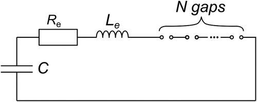
Note that the equivalent resistance Re depends on the current in the circuit (and, as a result, on the initial voltage); therefore, formula Equation(7)(7)
(7) is approximate. The equivalent resistance and inductance can be measured by approximating the current waveform with a damped oscillatory function
(8)
(8)
where ω and δ are the oscillation frequency and the damping decrement of the discharge current, respectively.
Formula Equation(7)(7)
(7) shows that the fraction of energy delivered to the interelectrode gaps increases with decreasing the capacitance (increasing the quality factor). However, it is not rational to reduce the capacitance too much, because this diminishes the pulse energy and, accordingly, the mass productivity of nanoparticles per pulse.
The fraction of energy delivered to the gaps also increases with a decrease in the initial voltage at the capacitive energy storage device, which can be achieved using a trigger pulse and a circuit with several gaps or a decrease in the gap length between the electrodes. When U0 is close to Udrop, the limit is reached; with a further decrease in the initial voltage, oscillations become impossible.
The fraction of energy transferred to the gaps also increases when several series-connected interelectrode gaps are employed. In this case, the dependence is not proportional since an increase in the number of gaps leads to a drop in the quality factor of the discharge circuit. Such disproportionality is clearly demonstrated by the calculations of the energy efficiency in SDGs with one and three interelectrode gaps, as shown in .
For the practical application of the proposed analytical model for determining the efficiency of energy transfer from the storage capacitor to the interelectrode gap in a spark discharge, it is important to represent the applicability limits of this model. Since the model is fundamentally based on the absence of the dependence of the voltage on the value of flowing current and the gap spacing, the limits of its applicability are the conditions for violation of this regularity for small and large values of discharge currents and capacitor energies.
Modes with an approximately constant voltage drop across the gap in the spark discharges with cold electrodes are characterized by the influx of current from the plasma column into the electrodes through one or many hot spots on the electrode, which randomly move, arise and disappear. Many publications are devoted to this phenomenon in vacuum and gas spark discharges. Electrode spots in gas discharges are strongly influenced by the gas and contamination layers on the electrode surface. The surface contaminants are capable of inducing new spots. Therefore, the spots are distributed over a large area and have diameters of less than 20 μm (Juttner Citation2001). The research on the erosion of the electrode surface (nickel and copper) on a single-spark level in the generation of aerosol nanoparticles at capacitor energies up to 50 mJ confirmed that several hundreds of craters are formed in each cycle of the discharge (Kohut et al. Citation2018). The crater diameter ranges from sub-micrometer to several tens of micrometers; their depth was found to linearly correlate with their diameter.
The lower limit of applicability of the proposed model at low pulsed discharge currents can be defined as the condition for the occurrence of a discharge with only one cathode spot. The formation of a spark discharge in the air between copper electrodes with a single cathode spot was realized and investigated (Parkevich et al. Citation2018). It was shown that a micron-sized (∼10 μm) cathode spot was formed during a time of the order of 2 ns at a current amplitude of about 3 A. According to the theoretical model, in order to provide a stable self-sustained discharge, the current per cathode spot should be approximately equal to 3.2 A (Gashkov et al. Citation2016).
On the top, the spark discharge modes with multiple independent electrode spots can be limited by two effects, either heating of the electrodes to high temperatures due to insufficient cooling at high average SDG power, or a strong effect of the magnetic field of the discharge current. The implementation of the first case depends on several conditions: the energy of the capacitor and the average SDG power, the material and cooling mode of the electrodes, the design of the discharge chamber. The second case is realized when the magnetic field pressure of the self-current on the plasma channel exceeds its hydrodynamic pressure and compresses the channel to a small diameter (Bogomaz et al. Citation2002). As a result, the hot spots on the electrodes are forced together and combined into one large hot spot. This leads to a high concentration of the energy density at the electrode and a manifold increase in the near-electrode voltage drop. At a peak current of 60 kA, the total voltage drop near the electrodes amounts to ∼500 V. The largest amplitudes of pulsed currents, at which the model proposed can be applied, do not exceed 10 kA.
In connection with the mechanism of electrode erosion resulting from of the action of many independent hot spots and the formation of craters on the electrode surfaces, a practically relevant question arises about the material fraction that turns into particles of submicron and micron sizes as compared with the synthesized nanoparticles. Large particles are assumed to be formed as a result of metal splashing out of the crater in the liquid phase, which is probably always due to the non-uniform heating of the electrode material in the area near the hot spot. The conditions, under which large particles are formed and under which they are not, have not been identified yet in systematic studies. It was suggested that there is a higher tendency of their formation with increasing the energy per spark (Pfeiffer et al. Citation2014). It is also possible to assume that a large fraction of large particles is generated by large craters, where the fraction of liquid metal is greater. In this line, it is necessary to look for pulsed discharge modes and requirements for electrodes, in which large craters do not arise. This problem seems to be relevant and should be the subject of a separate study.
Conclusion
It has been experimentally shown that the voltage across the active resistance of the interelectrode gap in a spark discharge weakly depends on the amplitude of the flowing current, and, for metal electrodes, it is of the order of several tens of volts. Practically, all the voltage drops occur in the near-electrode regions where the nanoparticle synthesis occurs. An algorithm for determining the energy transferred to the discharge gap was proposed. The energy released in this area can be only about 30% of the total energy stored in the storage capacitor. When designing generators with high efficiency of energy delivery to the discharge gap, one should also take into account the energy dissipation at the active resistance of the electrodes, the capacitor, and the connecting busbars. Finally, the energy transfer efficiency increases when several series-connected electrode gaps are employed, with a decrease in the capacitance of the energy storage device or a decrease in the initial voltage across it. The lower and upper approximate limits of applicability of the proposed model are governed by the value of the current amplitudes in the discharge. These limits are 3 and 10,000 A, respectively, provided that the proper cooling of the electrodes is ensured.
Additional information
Funding
References
- Arsenov, P. V., A. A. Efimov, and V. V. Ivanov. 2018. Effect of methods of changing in focusing ratio on line geometry in aerosol jet printing. Key Eng. Mater. 779:159–164. doi: 10.4028/www.scientific.net/KEM.779.159.
- Bazelyan, E. M., and Y. P. Raizer. 1997. Spark discharge. New York: CRC press.
- Bogomaz, A. A., A. V. Budin, V. A. Kolikov, M. E. Pinchuk, A. A. Pozubenkov, and F. G. Rutberg. 2002. Influence of the cathode and anode jets on the properties of a high-current electric arc. Tech. Phys. 47 (1):26–33. doi: 10.1134/1.1435886.
- Byeon, J. H., J. H. Park, and J. Hwang. 2008. Spark generation of monometallic and bimetallic aerosol nanoparticles. J. Aerosol Sci. 39 (10):888–896. doi: 10.1016/j.jaerosci.2008.05.006.
- Chakraborty, G., A. Sengupta, F. G. Requejo, and C. K. Sarkar. 2011. Study of the relative performance of silicon and germanium nanoparticles embedded gate oxide in metal–oxide–semiconductor memory devices. J. Appl. Phys. 109 (6):064504. doi: 10.1063/1.3555087.
- Cundall, C. M., and J. D. Craggs. 1955. Electrode vapour jets in spark discharges. Spectrochim. Acta 7 (3):149–164. doi: 10.1016/0371-1951(55)80018-5.
- Efimov, A. A., P. V. Arsenov, N. V. Protas, K. N. Minkov, M. N. Urazov, and V. V. Ivanov. 2018. Dry aerosol jet printing of conductive silver lines on a heated silicon substrate. IOP Conf. Series Mater. Sci. Eng. 307 (1):012082. doi: 10.1088/1757-899X/307/1/012082.
- Evans, D. E., R. M. Harrison, and J. G. Ayres. 2003. The generation and characterization of metallic and mixed element aerosols for human challenge studies. Aerosol Sci. Technol. 37 (12):975. doi: 10.1080/02786820300897.
- Feng, J., G. Biskos, and A. Schmidt-Ott. 2015. Toward industrial scale synthesis of ultrapure singlet nanoparticles with controllable sizes in a continuous gas-phase process. Scientific Rep. 5 (1):15788. doi: 10.1038/srep15788.
- Gashkov, M. A., N. M. Zubarev, O. V. Zubareva, G. A. Mesyats, and I. V. Uimanov. 2016. Model of liquid-metal splashing in the cathode spot of a vacuum arc discharge. J. Exp. Theor. Phys. 122 (4):776–786. doi: 10.1134/S1063776116040051.
- Guo, X., A. Gutsche, M. Wagner, M. Seipenbusch, and H. Nirschl. 2013. Simultaneous SWAXS study of metallic and oxide nanostructured particles. J. Nanopart. Res. 15 (4):1559. doi: 10.1007/s11051-013-1559-8.
- Hallberg, R. T., L. Ludvigsson, C. Preger, B. O. Meuller, K. A. Dick, and M. E. Messing. 2018. Hydrogen-assisted spark discharge generated metal nanoparticles to prevent oxide formation. Aerosol Sci. Technol. 52 (3):347–358. doi: 10.1080/02786826.2017.1411580.
- Han, K., W. Kim, J. Yu, J. Lee, H. Lee, C. G. Woo, and M. Choi. 2012. A study of pin-to-plate type spark discharge generator for producing unagglomerated nanoaerosols. J. Aerosol Sci. 52:80–88. doi: 10.1016/j.jaerosci.2012.05.002.
- Helsper, C., W. Mölter, F. Löffler, C. Wadenpohl, S. Kaufmann, and G. Wenninger. 1993. Investigations of a new aerosol generator for the production of carbon aggregate particles. Atmos. Environ. A. Gen. Topics 27 (8):1271–1275. doi: 10.1016/0960-1686(93)90254-V.
- Ivanov, V. V., A. A. Efimov, D. A. Myl’nikov, and A. A. Lizunova. 2018. Synthesis of nanoparticles in a pulsed-periodic gas discharge and their potential applications. Russian J. Phys. Chem. A 92 (3):607–612. doi: 10.1134/S0036024418030093.
- Ivanov, V. V., A. A. Efimov, D. A. Mylnikov, A. A. Lizunova, A. V. Bagazeev, I. V. Beketov, and S. V. Shcherbinin. 2016. High-Efficiency synthesis of nanoparticles in a repetitive multigap spark discharge generator. Tech. Phys. Lett. 42 (8):876–878. doi: 10.1134/S106378501608023X.
- Juttner, B. 2001. Cathode spots of electric arcs. J. Phys. D Appl. Phys. 34 :R103–R123. stacks.iop.org/JPhysD/34/R103.
- Kohut, A., L. Ludvigsson, B. O. Meuller, K. Deppert, M. E. Messing, G. Galbács, and Z. Geretovszky. 2017. From plasma to nanoparticles: optical and particle emission of a spark discharge generator. Nanotechnology 28(47):475603. doi: 10.1088/1361-6528/aa8f84.
- Kohut, A., M. Wagner, M. Seipenbusch, Z. Geretovszky, and G. Galbács. 2018. Surface features and energy considerations related to the erosion processes of Cu and Ni electrodes in a spark discharge nanoparticle generator. J. Aerosol Sci. 119:51–61. doi: 10.1016/j.jaerosci.2018.02.005.
- Krasnikov, D. V., B. Y. Zabelich, V. Y. Iakovlev, A. P. Tsapenko, S. A. Romanov, A. A. Alekseeva, A. K. Grebenko, and A. G. Nasibulin. 2019. A spark discharge generator for scalable aerosol CVD synthesis of single-walled carbon nanotubes with tailored characteristics. Chem. Eng. J. 372:462–470. doi: 10.1016/j.cej.2019.04.173.
- Lafont, U., L. Simonin, N. S. Tabrizi, A. Schmidt-Ott, and E. M. Kelder. 2009. Synthesis of nanoparticles of Cu, Sb, Sn, SnSb and Cu2Sb by densification and atomization process. J. Nanosci. Nanotechnol. 9 (4):2546–2552. doi: 10.1166/jnn.2009.dk13.
- Maisser, A., K. Barmpounis, M. B. Attoui, G. Biskos, and A. Schmidt-Ott. 2015. Atomic cluster generation with an atmospheric pressure spark discharge generator. Aerosol Sci. Technol. 49(10):886–894. doi: 10.1080/02786826.2015.1080812.
- Mesyats, G. A. 2004. Pulsed power engineering and electronics. Moscow: Nauka.
- Myl’nikov, D. A., V. V. Ivanov, A. A. Efimov, and I. V. Beketov. 2016. A technique for measurements of energy release in pulsed gas discharge in short interelectrode gaps. Measur. Techniq. 58 (12):1367. doi: 10.1007/s11018-016-0900-x.
- Mylnikov, D., A. Lizunova, V. Borisov, S. Paranin, and V. Ivanov. 2018. Germanium nanoparticles, synthesis in spark discharge. Oriental J. Chem. 34(5):2677–2680. doi: 10.13005/ojc/340563.
- Noh, S. R., D. Lee, S. J. Park, D. S. Kim, and M. Choi. 2017. High throughput nanoparticle generation utilizing High-Frequency spark discharges via rapid spark plasma removal. Aerosol Sci. Technol. 51(1):116–122. doi: 10.1080/02786826.2016.1239814.
- Ott, H. W. 1976. Noise reduction techniques in electronic systems. New York: John Wiley & Sons Canada, Limited.
- Pai, D. Z., K. K. Ostrikov, S. Kumar, D. A. Lacoste, I. Levchenko, and C. O. Laux. 2013. Energy efficiency in nanoscale synthesis using nanosecond plasmas. Scientific Rep. 3 (1):3. doi: 10.1038/srep01221.
- Palomares, J. M., A. Kohut, G. Galbács, R. Engeln, and Z. Geretovszky. 2015. A time-resolved imaging and electrical study on a high current atmospheric pressure spark discharge. J. Appl. Phys. 118(23):233305. doi: 10.1063/1.4937729.
- Parkevich, E. V., G. V. Ivanenkov, M. A. Medvedev, A. I. Khirianova, A. S. Selyukov, A. V. Agafonov, A. R. Mingaleev, T. A. Shelkovenko, and S. A. Pikuz. 2018. Mechanisms responsible for the initiation of a fast breakdown in an atmospheric discharge. Plasma Sources Sci. Technol. 27 (11):11LT01. doi: 10.1088/1361-6595/aaebdb.
- Pfeiffer, T. V. 2014. Towards the Industrial Application of Spark Ablation for Nanostructured Functional Materials. PhD. Diss., Delft University of Technology. p. 32.
- Pfeiffer, T. V., J. Feng, and A. Schmidt-Ott. 2014. New developments in spark production of nanoparticles. Adv. Powder Technol. 25 (1):56–70. doi: 10.1016/j.apt.2013.12.005.
- Rai, M., A. P. Ingle, S. Birla, A. Yadav, and C. A. D. Santos. 2016. Strategic role of selected noble metal nanoparticles in medicine. Critic. Rev. Microbiol. 42 (5):696–719. doi: 10.3109/1040841X.2015.1018131.
- Schwab, A. J. 1972. High-voltage measurement techniques. Cambridge, MA: M.I.T. Press.
- Slotte, M., and R. Zevenhoven. 2017. Energy efficiency and scalability of metallic nanoparticle production using arc/spark discharge. Energies 10 (10):1605. doi: 10.3390/en10101605.
- Tabrizi, N. S., M. Ullmann, V. A. Vons, U. Lafont, and A. Schmidt-Ott. 2009. Generation of nanoparticles by spark discharge. J. Nanopart. Res. 11 (2):315–332.
- Vons, V. A., L. C. Smet, D. Munao, A. Evirgen, E. M. Kelder, and A. Schmidt-Ott. 2011. Silicon nanoparticles produced by spark discharge. J. Nanopart. Res. 13 (10):4867–4879. doi: 10.1007/s11051-011-0466-0.
- Wagner, M., A. Kohut, Z. Geretovszky, M. Seipenbusch, and G. Galbács. 2016. Observation of fine-ordered patterns on electrode surfaces subjected to extensive erosion in a spark discharge. J. Aerosol Sci. 93:16–20. doi: 10.1016/j.jaerosci.2015.11.008.
- Yokomizu, Y., T. Matsumura, R. Henmi, and Y. Kito. 1996. Total voltage drops in electrode fall regions of, argon and air arcs in current range from 10 to 20 000 A. J. Phys. D Appl. Phys. 29 (5):1260. doi: 10.1088/0022-3727/29/5/020.
- Zhong, S., N. Miao, Q. Yu, and W. Cao. 2015. Energy measurement of spark discharge using different triggering methods and inductance loads. J. Electrostat. 73:97–102. doi: 10.1016/j.elstat.2014.10.014.