
Abstract
In this paper, the possibility of preparing silver nanostructures with a high area density of nanoparticles of various shapes by the ion beam sputtering (IBS) method, using a glancing angle deposition (GLAD) configuration, and subsequent irradiation with heavy ions, was tested. In the experiment, keV Ar+ ions were used for both IBS and bombardment. The prepared nanostructures were analyzed by RBS and microscopic methods of SEM and AFM. It turned out that IBS/GLAD makes it possible to create silver nanostructures (networks of individual silver nanoparticles), but only with relatively low areal densities (∼ 70 µm2). The bombardment led to changes in the porosity only after high ion fluences, but also to disruption of the nanostructures. Even so, the IBS method with GLAD configuration has been shown to be a promising way to prepare high-porosity nanostructures. Nevertheless, further experimental efforts will be needed to find the optimal technology.
Introduction
With the development of smart deposition technologies (Citation1), new complex mono- and multi-component materials with defined nanostructures are attracting increasing interest from the scientific community due to their unique properties and great application potential. Besides, scientists have always been interested in the dependence of the physical properties of nanostructures (nanoparticles) on their size, which is often very different from their bulk counterparts (Citation2). For the synthesis of nanoscale materials, approaches generally referred to as bottom-up and top-down have been rapidly developed in recent decades (Citation3). Thus, using such deposition strategies, various sophisticated nanostructure architectures have been created so far (Citation4). Also, with the development of ion and laser beam technologies (Citation5, Citation6), ion and laser irradiation has established itself as promising techniques for creating or modifying specific surface morphologies and thin film nanostructures, see, e.g. (Citation7, Citation8). Although our understanding of phenomena occurring during ion and laser irradiation (or ion implantation and sputtering) of materials, whether bulk or thin films, is insufficient (Citation9–12), these methods, anyway, are one of the most important technologies that make it possible to create complex nanostructures that are difficult to prepare in other ways (Citation13). Further, one of the application-important parameters of fabricated thin-film nanostructures is their surface-to-volume ratio (Citation14). It is an aspect that plays a significant role in porous or irregular nanostructures, where it determines their electrocatalytic, sensing and other capabilities (Citation15). Such nanostructures also include the ‘black metals’, attractive materials synthesized usually as porous, mono-elemental metallic thin films that exhibit enhanced absorption of light, which makes them antireflective to a high degree (Citation16).
In this work, a study of the synthesis of thin silver-based nanostructures and their modification by low-energy heavy ion irradiation was carried out in order to prepare silver films with a high porosity (considered as high areal density of nanoparticles of different shape) that would be close to black metals. The purpose of the study was to investigate and confirm whether it is possible to prepare such nanostructures by ion beam sputtering a silver target at a very oblique angle (Citation17), with possible subsequent irradiation of the deposited film with a high fluence heavy ion beam.
Materials and methods
The synthesis of thin Ag films was carried out by Ion Beam Sputtering (IBS) method using Ar+ ions bombarding the Ag target (MSE Supplies, 99.99% purity) fixed on a revolving sample holder mounted in the center of the IBS vacuum chamber with a base pressure of 3 × 10⁻⁶ mbar. The IBS deposition was carried out in a low-energy ion facility installed in the NPI CANAM infrastructure (Figure a). In the facility, intense beams of gas ions (e.g. N+, Ar+, Xe+) can be generated using a duoplasmatron source with currents of up to tens of mA and energy from 100 eV to 35 keV. A beam of singly charged Ar+ ions was used for this study with a selected extraction voltage of 20 kV with a current (measured at the target position) of 0.8 mA.
Figure 1. a) Sketch of a low-energy ion facility generating Ar+ ions with a selected energy 10 and 20 keV, and a current of 1 mA; b) sketch of ion sputtering of a silver target on a Si substrate mounted on a stepping motor rotating at 3 rpm. The angle of incidence of the sputtered Ag species on the Si substrate was kept at an angle of 87° (the angle between the target normal and the substrate normal).
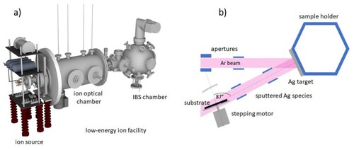
The Ag films were synthesized on the Si <100 > wafer substrates (5 × 5 cm2, supplied by Ted Pella) using a Glancing Angle Deposition (GLAD) configuration. The angle between the sputtering silver target (Kurt J. Lesker; 99.99% pure, density 10.49 g/cm3) and the Ar+ ion beam (with a diameter ∼ 10 mm, defined by a set of apertures) was kept fixed at 30° (the sputter yield for this arrangement is about 10 atoms/ion (Citation18)), the angle between the normal to the target and the normal to the substrate was ∼ 87°. The distance between the Ag target and the Si substrate (center to center) was 10 cm. The substrates were fixed on a platform of the high-vacuum stepping motor that was revolving during deposition at an angular speed of 3 rpm. The experimental setup is shown in Figure b.
From the stated sputtering yield and the set-up geometry, it is possible to obtain an estimate of the deposition rate and the thickness of the synthesized Ag layer. In the normal direction (the substrate and target are oriented co-axially 10 cm apart) the geometric factor (a solid angle between the target and the substrate) is about 0.25×10⁻², i.e. the deposition rate corresponds to ∼ 0.25×10⁻¹ Ag atoms/Ar ion. For an applied ion beam current of 0.8 mA this corresponds to about 1.25×10¹⁴ Ag atoms/s (i.e. to 0.04 nm/s, assuming the density of the deposited layer is the same as that of bulk silver). For a typical IBS, lasting 1 h, the thickness of the Ag layer should be approximately 140-150 nm. However, because of the unusual GLAD configuration (i.e. substrate with an 87° inclination to the target), the geometric factor is reduced by 20 times (to about 0.01×10⁻²). In that case, the total thickness of the Ag layer would be only about 10 nm. However, since nanoparticles of different sizes are formed on the substrate during deposition, the result is a nanostructure of interconnected nanoparticles with an irregular morphology, the thickness of which can reach tens of nm in some random places.
After deposition, the same ion beam facility was also used to irradiate the fabricated Ag nanostructures with Ar+ ions at an energy of 10 keV in the normal direction (in this case, the sputter yield corresponds to ∼ 8 atoms/ion (Citation19, Citation20)). For this purpose, the samples were placed at the position of the sputtering target; each sample was irradiated with a different fluence, including high-level fluences, namely 2.4 × 10¹⁶ Ar+/cm2 and 2.7 × 10¹⁷ Ar+/cm2.
The chemical composition, morphology, and thickness of the as-deposited and irradiated films were analyzed using several relevant methods: Rutherford Back Scattering (RBS, using 2 MeV alpha particles) and Atomic Force Microscopy (AFM, with a tapping mode) (NT-MDT, NTEGRA Aura) at the NPI CANAM infrastructure (Citation21), and Scanning Electron Microscopy (SEM) (JEOL, Model JSM-7200F, 15-20 kV) at Charles University in Prague (Citation22).
Results and discussion
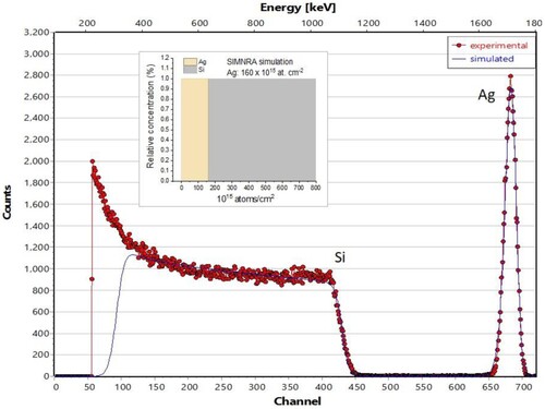
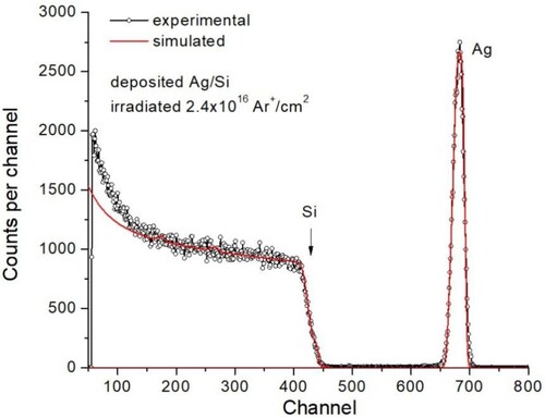
Figure shows the result of the RBS measurement performed using 2 MeV alpha particles at the 3 MeV Tandetron accelerator at NPI Rez (Citation21). The result of the measurement confirms that using a combination of IBS with a GLAD approach, an Ag layer is formed on the Si substrate with a thickness (according to the SIMNRA simulation (Citation23)) of about 160 × 1015 at. Ag/cm2 (see the inset in Figure ), which corresponds to approx. 50 nm (if it is considered that the density of the silver layer is 10.49 g/cm3).
Figure 2. RBS analysis (using 2 MeV alpha particles) of the Ag/Si sample and a SIMNRA simulation (the inset shows a depth profile: step dependence of the relative concentration of elements on depth in 1015 atoms/cm2 units). The silver layer was deposited on the Si substrate by sputtering of Ag species (atoms, clusters) from a silver target using 20 keV Ar+ ions with a current of 0.8 mA and using a GLAD set-up configuration.
However, the RBS with an ion probe of approximately 1 mm in a beam diameter does not allow for determining the lateral distribution of the silver layer. The method only provides information about the average value of the depth profiles of elements in the sample, in this case, about the average thickness of the deposited Ag layer - it is not assumed that the sputtered Ag species with a nominal energy of only a few keV would penetrate more than a few nm into the Si substrate during their landing (SRIM (Citation24)). Therefore, SEM and AFM microscopic methods were used for further analyses.
Figure shows micrographs of the top and side views of the nanostructure prepared (similarly as for the RBS study) by ion beam sputtering of the Ag target using a GLAD configuration where the substrate (Si <100 > wafer) was fixed on a rotary holder of a stepping motor (rotating in a vacuum chamber at a low speed of 3 rpm) at an angle (between the substrate normal and the target normal) of 87°. This angle was chosen based on the results of a work (Citation25), where a first attempt was made to prepare a porous gold nanostructure using the magnetron sputtering method. The authors took advantage of atomic shadowing effects (Citation26), using viewing angle deposition, and created distinctive nanostructured coatings. Since the Ag species (atoms, clusters) are sputtered from the target to different angles, a set of apertures was placed between the substrate and the target to limit the Ag deposition at angles outside the sector of 87° ± 3°. As can be seen from the SEM micrographs of Figure , the formed nanostructure consists of isolated irregular silver particles with a size of approx. 100-400 nm and a thickness of approx. 60 nm. Interestingly, the formed grains have a various (round, oval, elongated) shape with no signs of crystalline facets. The obtained morphology is very different from that which can be obtained by IBS deposition at smaller angles or at a normal direction – i.e. a smooth, thin and continuous Ag layer with a low roughness.
Figure 3. SEM micrographs of the Ag nanostructure (i.e. a) – top view, and b) – side view, prepared by sputtering of an Ag target (using 20 keV Ar+ ions with a current of 0.8 mA) on a Si wafer in a GLAD configuration.
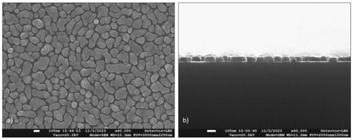
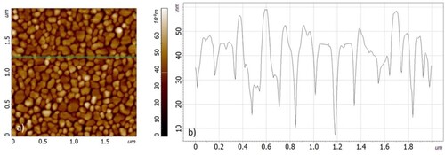
Figure shows the surface morphology (a) and height profile (b) along the green line (a) of the prepared nanostructure analyzed by AFM. This analysis confirms the data from the SEM measurements, i.e. the nanostructure consists of isolated grains (with an area density of about 75 µm-2) with different lateral sizes (approx. 50 - 200 nm, in some cases the grain size reaches approx. 300 nm) and thicknesses (approx. 40 - 50 nm, in some cases the thickness reaches approx. 60 nm). Also, from the AFM view, the grains have sharper edges, and no facets were observed anywhere (even at a higher AFM magnification).
Figure 4. AFM surface morphology (a), and height profile (b) along the green line of the Ag nanostructure prepared by ion sputtering of an Ag target (using 20 keV Ar+ ions with a current of 0.8 mA) on a Si wafer in a GLAD configuration.
Thus, it turns out that nanostructures, formed as networks of individual isolated silver particles (grains) with a size of 50 - 400 nm, can be created by the method of sputtering of the Ag target with heavy keV ions using an arrangement of the glancing angle deposition. In fact, such irregular nanostructures may exhibit properties of black metals that could be useful in some applications mentioned in the introduction. However, in order to highlight the properties even more, it would be necessary to enhance the porosity of the nanostructures, i.e. their surface-to-volume ratio.
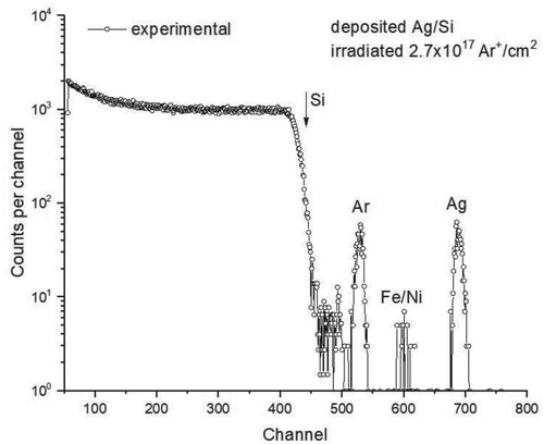
In the next step, therefore, an unconventional way of modification of the Ag nanostructures – by ion bombardment with heavy ions in a perpendicular direction (at an oblique angle, rapid destruction of the sample would occur) – was tested. For irradiation, an Ar+ 10 keV/1 mA beam was applied (10 keV Ar+ ions can penetrate through the synthesized Ag nanostructure to the Si substrate), with a wide range of fluence from 1015 to a few times 1017 Ag+/cm2. Surprisingly, it turned out that for fluences up to about 1016 cm-2, there are no observable changes, not only in the morphology of the nanostructure but also in the elemental composition and the total amount of the Ag deposit in the sample. The changes only become apparent well above the 1016 Ag+/cm2 irradiation level, and once the 1017 Ag+/cm2 level is reached, the surface morphology of the Ag nanostructure breaks down, and the amount of deposited silver decreases rapidly. This is evidenced by the results of all applied diagnostic methods. Figure shows the RBS analysis for a sample irradiated with a 10 keV Ar+ beam with a fluence of 2.4 × 1016 cm-2, which confirms that even for such a relatively high fluence, the depth distribution of Ag remains unchanged (i.e. basically identical to the non-irradiated sample, see Figure ).
Figure 5. RBS analysis (with 2 MeV alpha particles) of the Ag/Si sample irradiated perpendiculalry with 10 keV Ar+ ions with the fluence 2.4 × 1016 cm-2. The silver layer was deposited on the Si substrate by sputtering of Ag from a silver target using 20 keV Ar+ ions with a current of 0.8 mA and in a GLAD set-up configuration.
This conclusion is supplemented by the AFM analysis in Figure , where the surface morphology of the sample is shown together with the analysis of the height profile in the indicated direction (see the green line). Here, too, one can see (compared with Figure ) that the surface pattern did not change after irradiation (the size of the particles also reaches several hundred nm, the range of thicknesses is the same, and the area density of the particles is also around 75 µm-2). As can be seen, even after irradiation of the sample with a multiple overlapping fluence (each nm of the surface is hit by heavy ions at least 100x), the Ag nanostructure is preserved. However, as already mentioned, above this level, rapid erosion of the structure begins, and at an order of magnitude higher fluence (1017 Ag+/cm2), the nanostructure completely disintegrates - there is a massive loss of Ag and, as a result, also a reduction in both the area density of nanoparticles (approx. 50 µm-2), and their reduction in lateral dimension (< 100 nm) and especially in their thickness (< 25 nm). In addition, however, the presence of Ar+ projectiles, which penetrate the Ag layer and anchor in the Si substrate, is evident. In the RBS spectra, the presence of Ar is shown as a rising peak between the decreasing Ag peak and the Si edge (Figure ). In addition to the Ar line, a Fe/Ni signal can also be observed due to contamination originating from the sputtered aperture material limiting the size of the Ar+ ion beam.
Figure 6. AFM surface morphology (a), and height profile (b) along the green line of the Ag nanostructure prepared by ion sputtering of an Ag target (using 20 keV Ar+ ions with a current of 0.8 mA) on a Si wafer in a GLAD configuration, and subsequent irradiation of the nanostructure with 10 keV Ar+ ions with a fluence of 2.4 × 1016 cm-2.
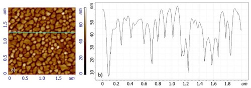
Figure 7. RBS analysis (2 MeV alpha particles) of the Ag/Si sample irradiated perpendiculalry with 10 keV Ar+ ions with a fluence of 2.7 × 1017 cm-2. The Ag layer was deposited on the Si substrate in a GLAD set-up configuration by sputtering of an Ag target using 20 keV Ar+ ions with a current of 0.8 mA. In addition to Ag and Si, there is also a signal from Ar (due to Ar+ bombardment) and Fe/Ni (due to contamination from the apertures) in the spectrum.
Structural changes are visible both in SEM micrographs (Figure ) and AFM (Figure ). The main changes observed in Ag nanostructures after irradiation with the highest fluences are shown in Table .
Figure 8. SEM micrographs of the Ag nanostructure (i.e. a) – top view, and b) – side view, prepared by sputtering of an Ag target (using 20 keV Ar+ ions with a current of 0.8 mA) on a Si wafer in a GLAD configuration, after irradiation with the 10 keV Ar+ ions with a fluence of 2.7 × 1017 cm-2.
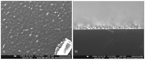
Figure 9. AFM morphology (a), and height profile (b) along the green line (a) of the Ag nanostructure prepared by ion sputtering of an Ag target (using 20 keV Ar+ ions with a current of 0.8 mA) on a Si wafer in a GLAD configuration, and subsequent irradiation with 10 keV Ar+ ions with a fluence of 2.7 × 1017 cm-2.
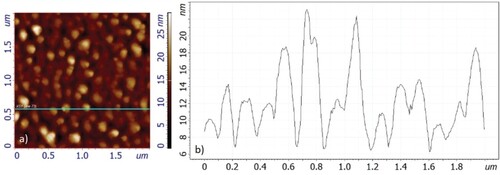
Table 1. Main changes in the Ag nanostructures after Ar+ ion irradiation with high fluences.
Conclusion
The work dealt with the question of whether it is possible to use the Ion Beam Sputtering (IBS) method to create silver nanostructures that would exhibit high porosity (considered as a high density of particles with various shapes), so that their application could be considered in areas which require a large surface-to-volume ratio. For this purpose, the atomic shielding effect requiring deposition at a very oblique angle was utilized, which was recently successfully applied in the preparation of gold nanostructures with high porosity using magnetron sputtering. The IBS method has only been slightly tested so far, and that was the main motivation for this work. In the paper was demonstrated that IBS using the Glancing Angle Deposition (GLAD) configuration can indeed create Ag nanostructures in the form of separated Ag nanoparticles (however, with a size of several hundred of nm and areal density of about 75 µm2). To increase the porosity, the synthesized Ag nanostructures were irradiated with keV Ar+ ions with the intention of fragmenting the Ag nanoparticles. It was shown that the structural changes do occur, but only after very high fluences exceeding 1016 Ar+/cm2. On the one hand, this is a surprising effect of high radiation resistivity of the Ag nanostructures prepared by IBS/GLAD; on the other hand, the increase in porosity was not observed (or was not as pronounced), the high fluence rather resulted in a rapid destruction (by sputtering) of the Ag nanostructure. Since the formation of nanostructures with a high surface-to-volume ratio depends on several parameters (ion energy, ion impact angle on the target, GLAD configuration, substrate rotation speed, etc.), it will be necessary to investigate their influence on determining the optimal technology. This will, of course, require further experimental effort.
Acknowledgements
The authors also thank Mrs. S.A. Vacik for proofreading.
Disclosure statement
No potential conflict of interest was reported by the author(s).
Additional information
Funding
References
- Handbook of Deposition Technologies for Films and Coatings: Science, Applications and Technology: Martin, Peter M., Ed.; William Andrew: New York, 2009.
- Baig, N.; Kammakakam, I.; Falath, W. Nanomaterials: A Review of Synthesis Methods, Properties. Recent Progress, and Challenges. Mater. Adv 2021, 2, 1821–1871.
- Szczyglewska, P.; Feliczak-Guzik, A.; Nowak, I. Nanotechnology–General Aspects: A Chemical Reduction Approach to the Synthesis of Nanoparticles. Molecules 2023, 28 (13), 4932.
- Nano-Architectured and Nanostructured Materials: Fabrication, Control and Properties: Champion, Yannick, Ed.; Hans-Jörg Fecht, Wiley-VCH: Weinheim, 2005.
- Nastasi, M.; Mayer, J.W.; Wang, Y. Ion Beam Analysis: Fundamentals and Applications; CRC Press: Boca Raton, 2014.
- Laser Beams: Theory, Properties and Applications (Lasers and Electro-Optics Research and Technology), Thys, Maxim, Desmet, Eugene, Eds.; Nova Science Pub Inc; UK ed. Edition: New York, (2010).
- Vacík, J.; Horák, P.; Bakardjieva, S.; Bejsovec, V.; Ceccio, G.; Cannavo, A.; Torrisi, A.; Lavrentiev, V.; Klie, R. Ion Sputtering for Preparation of Thin MAX and MXene Phases. Radiat. Eff. Defects Solids 2020, 175 (1-2), 177–189.
- Picciotto, A.; Torrisi, L.; Margarone, D.; Bellutti, P. Radiation Effects. Defects in Solids: Inc. Plasma Sci. & Plasma Tech 2010, 165 (6-10), 706–712.
- Zinkle, S.J.; Snead, L.L. Opportunities and Limitations for ion Beams in Radiation Effects Studies: Bridging Critical Gaps Between Charged Particle and Neutron Irradiations. Scr. Mater. 2018, 143, 154–160.
- Ziegler, J.F. Ion Implantation Science and Technology; Academic Press: NY, 2012.
- Sputtering by Particle Bombardment I: Physical Sputtering of Single-Element Solids, Behrisch, R., Ed.: Springer-Verlag Ed.: Berlin, (2013).
- Sputtering by Particle Bombardment II: Sputtering of Alloys and Compounds, Electron and Neutron Sputtering, Surface Topography, Behrisch, R., Ed.; Springer-Verlag: Berlin, 2013.
- Gates, B.D.; Xu, Q.; Stewart, M.; Ryan, D.; Willson, C.G.; Whitesides, G.M. New Approaches to Nanofabrication: Molding, Printing, and Other Techniques. Chem. Rev 2005, 105, 1171–1196.
- Zhao, Y.P.; Wang, F.C. Surface Tension Effects of Nanostructures, In Encyclopedia of Nanotechnology: Bhushan, B., Eds.; Springer: Dordrecht, 2016.
- Aralekallu, S.; Sannegowda, L.K. Handbook of Nanomaterials for Sensing Applications, In Micro and Nano Technologies: Hussain, C.M., Kailasa, S.K., Eds.; Elsevier: Amsterdam, 2021; pp 589–629.
- Christiansen, A.B.; Caringal, G.P.; Clausen, J.S.; Grajower, M.; Taha, H.; Levy, U.; Mortensen, N.A.; Kristensen, A. Black metal thin films by deposition on dielectric antireflective moth-eye nanostructures. Sci. Rep. 2015, 5. Article number: 10563.
- Vitrey, A.; Alvarez, R.; Palmero, A.; González, M.U.; García-Martín, J.M. Fabrication of Black-Gold Coatings by Glancing Angle Deposition with Sputtering. Beilstein J. Nanotechnol 2017, 8, 434–439.
- Sarkar, J. Sputtering Materials for VLSI and Thin Film Devices 2014, In Chapter 2 - Sputtering and Thin Film Deposition; Sarkar, J., Ed.; William Andrew: New York, 2014; pp 93–170.
- Yamamura, Y.; Tawara, H. At. Data Nucl. Data Tables 1996, 62, 149–253.
- www2.iap.tuwien.ac.at/www/surface/sputteryield.
- www.ujf.cas.cz/en/research-development/large-research-infrastructures-and-centres/canam/about-the-project/.
- www.mff.cuni.cz/cs/kmf/experimentalni-vybaveni/mikroskopicke-metody.
- Mayer, M. An Expert-Assisted System for Improving the Quality of IBA Simulations by SIMNRA. J. Phys. Conf. Ser. 2022, 2326, 012007.
- Ziegler, J.F.; Biersack, J.P.; Littmark, U. The Stopping and Range of Ions in Solids; Pergamon: New York, 1985.
- Vitrey, A.; Alvarez, R.; Palmero, A.; González, M.U.; García-Martín, J.M. Fabrication of Black-Gold Coatings by Glancing Angle Deposition with Sputtering. Beilstein J. Nanotechnol 2017, 8, 434–439.
- Liu, H.; Ma, D.; Li, Y.; You, L.; Leng, Y. Evolution of the Shadow Effect with Film Thickness and Substrate Conductivity on a Hemispherical Workpiece During Magnetron Sputtering. Metals 2023, 13 (1), No. 165.