
 ?Mathematical formulae have been encoded as MathML and are displayed in this HTML version using MathJax in order to improve their display. Uncheck the box to turn MathJax off. This feature requires Javascript. Click on a formula to zoom.
ABSTRACT
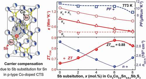
Heavily acceptor-doped Cu2SnS3 (CTS) shows promisingly large power factor (PF) due to its rather high electrical conductivity (σ) which causes a modest ZT with a high electronic thermal conductivity (κe). In the present work, a strategy of carrier compensation through Sb-doping at the Sn site in Cu2Sn0.8Co0.2S3 was investigated, aiming at tailoring electrical and phonon transport properties simultaneously. Rietveld analysis suggested a complex polymorphic microstructure in which the cation-(semi)ordered tetragonal phase becomes dominant over the coherently bonded cation-disordered cubic phase, as is preliminarily revealed using TEM observation, upon Sb-doping and Sb would substitute Sn preferentially in the tetragonal structure. With increasing content of Sb, the σ was lowered and the Seebeck coefficient (S) was enhanced effectively, which gave rise to high PFs maintained at ~10.4 μWcm−1K−2 at 773 K together with an optimal reduction in κe by 60–70% in the whole temperature range. The lattice thermal conductivity was effectively suppressed from 1.75 Wm−1K−1 to ~1.2 Wm−1K−1 at 323 K while maintained very low at 0.3–0.4 Wm−1K−1 at 773 K. As a result, a peak ZT of ~0.88 at 773 K has been achieved for Cu2Sn0.74Sb0.06Co0.2S3, which stands among the tops so far of the CTS-based diamond-like ternary sulfides. These findings demonstrate that polymorphic microstructures with cation-disordered interfaces as an approach to achieve effective phonon-blocking and low lattice thermal conductivity, of which further crystal chemistry, microstructural and electrical tailoring are possible by appropriate doping.
Graphical Abstract
1. Introduction
Thermoelectric (TE) materials can convert a temperature gradient into an electrical voltage and vice versa, by utilizing the Seebeck effect and Peltier effect, respectively [Citation1]. They can be used both in applications for thermal energy recovery from various heat resources [Citation2] and for steady-state cooling for electronic devices [Citation3,Citation4], and therefore have been attracting wide attentions for decades [Citation5]. The thermal-to-electric conversion efficiency for a TE material is determined by the dimensionless figure of merit, ZT = S2σT/(κe + κl) [Citation6], where the S, σ, T are Seebeck coefficient, electrical conductivity, and the absolute temperature, respectively, and the κe and κl are the electronic and the lattice components, of which the sum represents the total thermal conductivity, κ, for a TE material. In particular, from the viewpoint of scalable commercial application, intensive efforts have been made in research of TE materials beyond the currently most-widely used heavy alloys, such as compounds of Te, Bi, Pb and etc., most of which are naturally scarce and/or toxic. Thus, a multitude of environmentally friendly thermoelectric sulphides has been reported, such as chalcopyrite CuFeS2 [Citation7,Citation8], tetrahedrite [Citation9,Citation10], paracostibite CoSbS [Citation11,Citation12] and thiospinels [Citation13–15].
Mohite-type diamond-like ternary compound of Cu2SnS3 (hereafter CTS) has emerged as a new environmental-friendly candidate in recent years due to its phonon-glass-electron-crystal characteristics [Citation16–18] among the high-performance TE sulfides such as synthetic colusites [Citation19,Citation20]. Structurally, phase transition after doping is common and has already been reported in several references [Citation21–25], and in our samples, it adapts three different variants including monoclinic, cubic and tetragonal phases (hereafter referred to as m-CTS (a = 6.653 Å, b = 11.537 Å, c = 6.665 Å [Citation26]), c-CTS (a = b = c = 5.43 Å) and t-CTS (a = b = 5.413 Å, c = 10.824 Å [Citation27]), respectively) with the space group of Cc, F-43 m and I-42, respectively. According to the theoretical work by Zhang et al. [Citation16], m-CTS is a direct-gap semiconductor containing three bands deriving from the strong hybridization between Cu-3d and S-3p orbitals in the valence band edge and one single band from Sn-4s in the conduction band (CB) edge, which means clearly the priority for p-type TE performance with a 3D hole transport channel mainly consisting of Cu-S and S-S networks, and moreover, the benefit for carrier concentration optimization by alloying and/or doping at the Sn site that can help suppress κl while deteriorating little the electrical conduction. Meanwhile, it has a very low intrinsic κl at high temperatures which approaches its theoretical minimum of about 0.3 W m−1 K−1 at 773 K, suggesting a promising prospective for mid-temperature TE applications.
Indeed, experimental research indicated that heavily acceptor-doping using transition metals, such as Zn [Citation17], Ni [Citation28], Mn [Citation21], Fe [Citation18], Cu [Citation29], In [Citation30] etc., can cause a structural transformation from cation-order low-symmetry (m-CTS) to disorder high-symmetry (t-CTS and c-CTS) phases which not only helps to reach an ultralow κl due to the strengthened anharmonicity, but also optimize the transport properties through band engineering and the enhanced carrier concentration, synergistically giving rise to high power factors (PF = S2σ) of ~8.0 μW cm−1 K−2 and maximal ZT values of about 0.6–0.7 around 773 K. Moreover, a similar result can even be obtained in the recent report via ab initio calculation without resorting to chemical alloying [Citation31]. Particularly, acceptors with unfilled d-orbitals (e.g. Co [Citation32] and Mn [Citation19]) are found to be able to enhance the carrier DOS (density-of-states) effective mass m*, possibly due to the participation of their d-orbitals in the upper valence bands, resulting in even higher PFs of 9.0 ~ 11.0 μW cm−1 K−2 at high temperatures and a peak ZT of 0.85 at 723 K in 20%Co-doped CTS (Cu2Sn0.8Co0.2S3).
However, heavy doping for CTS usually causes a highly degenerate state with a large σ, up to 1500 S cm−1 around 300 K, and consequently a considerable κe up to 0.9–1.0 W m−1 K−1, which accounts for over ~2/3 of the total κ and limits the ZT noticeably. Thus, it should be a feasible way to enhance the TE performance by properly lowering the σ while maintaining the high PF.
In the present work, an approach of carrier compensation through donor-doping at Sn site using Sb is put forward for Cu2Sn0.8Co0.2S3 to examine the effect in tailoring the electrical transport properties as mentioned above, in view of that the Sb substitution for Sn can generate electrons which would help reduce the high hole carrier concentration by electron-hole recombination while affecting little the conducting states, and in addition, suppress the lattice thermal conductivity due to the high-entropy effect.
2. Experiment
Powder samples with a nominal composition of Cu2Sn0.8−xSbxCo0.2S3 (x = 0, 0.02, 0.04, 0.06, 0.08) were prepared by high temperature reaction. First, high purity element powders of Cu, Sn, Sb, Co and S were weighed and mixed thoroughly in a mole ratio of 2: 0.8-x: x: 0.2: 3. The mixtures were sealed under high vacuum in silica tubes and heated in a box furnace at a rate of 5 K min−1 to 1193 K, held there for 8 h, then rapidly cooled to 983 K and kept for 48 h, finally the mixtures were cooled down naturally to room temperature to obtain the compound ingots. The synthesized ingots were thoroughly ground into powders in an Al2O3 mortar, and then sieved. The powders were sintered into compact pellets (over 95% theoretical density) in graphite dies at 823 K for 5 min under an axial pressure of 50 MPa and vacuum (< 5 Pa) by spark plasma sintering (SPS).
The phase composition and crystal structure of the samples were checked by X-ray diffraction (XRD) analysis with an ARL X’TRA diffractometer (SmartLab3, RIGAKU, Japan) using Cu Kα radiation. Sample’s morphology was observed by field-emission scanning electron microscopy (FE-SEM, FEI Nova NanoSEM450). The microstructure was conducted using a transmission electron microscopy (JEM-2100 F). The Seebeck coefficients and electrical conductivities were measured in the radial direction of a bar-shaped specimen with dimensions of 10 mm × 2 mm × 3 mm by a conventional steady state method and a four-probe method, respectively, in a He atmosphere at 323 to 723 K with a commercial system (LSR-3, Linseis). X-ray photoelectron spectroscopy (XPS) was performed with a Physical Electronics system (ESCALAB 250Xi) using a standard Al Kα source. Thermal conductivity was calculated by ĸ = DρCp, where the D was thermal diffusivity measured in the axial direction of a disk-shaped sample of Φ 10 mm × 1 mm using a Netzsch laser flash diffusivity instrument (LFA457, Netzsch, Germany), the Cp was the specific heat capacity calculated according to the Dulong–Petit law [Citation33], and ρ was the mass density measured using the Archimedes method. Hall effect measurements for the carrier concentration and Hall mobility were conducted with a van der Pauw configuration under vacuum using a ResiTest8300 system (Toyo Tech. Co., Japan). The uncertainties of S and σ measurements are ±3 and ±5%, respectively, leading to a PF error of ±10%. Combining with the uncertainty of ±10% for κ measurements, the error bar of ZT is estimated to be no more than ±20%.
3. Results and discussion
) shows XRD patterns for all the Cu2Sn0.8-xSbxCo0.2S3 (x = 0, 0.02, 0.04, 0.06 and 0.08) bulk samples, together with illustrations of crystal structures for the cubic and tetragonal phases (). All the samples, as can be seen, are basically composed of t-CTS and/or c-CTS phases when x is less than 0.06. With x ≥ 0.06, peaks (222) and (440) for Cu3SbS3 (PDF#27-1745) at 30° and 50° are found. In the c-CTS, the cations are completely disordered at the 4a sites, statistically of 2/3 Cu and 1/3 Sn, and in the t-CTS, the 2a sites are occupied by 3/8 Cu and 5/8 vacancy, and the 2b and 4d sites by composite atoms of M1[43.6%Sn+56.4%Cu] and M2[46.3%Sn+53.7%Cu], respectively. This means that in these doped CTS, the cations including Cu, Sn, and Co and Sb are semi-ordered in t-CTS or fully disordered in c-CTS, which contributes significantly to achieve the very low κl. Moreover, the improved symmetry of the S-centered SM4 (M = metal atoms) tetrahedra compared to that in the m-CTS structure should be also beneficial to give an enhanced degeneracy of the orbitals in the upper VB and thus an increase of DOS near the Fermi level.
Figure 1. XRD patterns of (a) the Cu2Sn0.8-xSbxCo0.2S3 (x = 0, 0.02, 0.04, 0.06 and 0.08) bulk samples and (b) the enlarged area from 29° to 31° in (a), together with the crystal structure illustrations of the (c) cubic and tetragonal phases
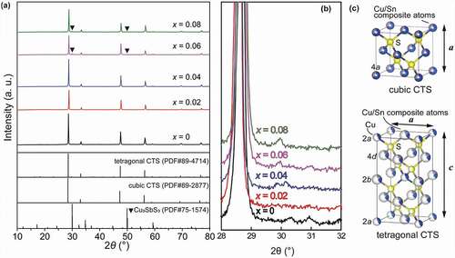
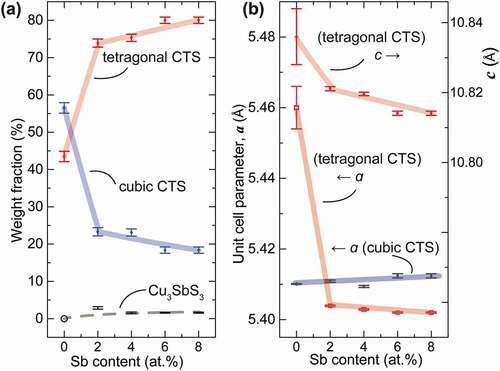
To analyse the change of phase composition and crystal structure due to Sb doping, Rietveld refinement was conducted using a BGMN-cored program Profex [Citation34] with these 3 phases taken into account, which adopted a polymorphic model consisting of c-CTS, t-CTS and m-CTS phases and ended with a low Rwp of 3.1–4.3% (in ) suggesting high goodness-of-fitting. (see Figure S1 for the Rietveld refinement result of x = 0.06 sample) As summarized in , the weight fraction of t-CTS increased abruptly from about 45 wt.% to about 75% in the x = 0.02 sample, then gradually to 80% at x = 0.08. Correspondingly, the fraction of the c-CTS phase dropped largely from about 55 to 22% with x = 0.02, then gradually to about 18% with x increasing to 0.08. Meanwhile, the amount of impurity Cu3SbS3 was kept at a very low level of ~1.6%. This result indicates t-CTS phase was much favored upon Sb substitution. Moreover, as shown in ), the unit cell parameter, a, increased very little, while a and c contracted drastically with 0.02 at% Sb incorporation, and were further reduced with increasing x. This agrees well with relatively smaller ionic radius of Sb5+ (60 pm for coordination number C.N. = 6) than that of Sn4+ (69 pm for C.N. = 6), and suggests strongly that the Sb substitution should take place predominantly in the t-CTS phase. More interestingly, this signifies that Sb-doping might have caused a remarkable change in the coordination configuration of SM4 tetrahedra in t-CTS phase.
Table 1. The weight fractions of the c-CTS, t-CTS and Cu3SbS3 phases, the lattice parameters of a, b and c of the two CTS phases, and the Rwp derived from Rietveld refinement of the XRD data
Figure 2. (a) The weight fractions of the c-CTS, t-CTS and Cu3SbS3 phases, and (b) the lattice parameters of a and c of the two CTS phases, derived from Rietveld refinement of the XRD data. Note that in the refinement the nominal composition of Cu2SnS3 were used for simplicity
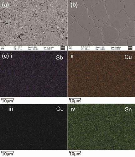
However, we didn’t find any obvious inhomogeneity of elemental distribution by SEM and energy-dispersive X-ray spectroscopy (EDX). As shown in and b) for the SEM images for thermally etched mirror surface of the merely Co-doped CTS and the x = 0.08 sample, respectively, no remarkable difference in grain growth has been found due to the Sb substitution. EDX mappings revealed homogeneous distribution of all elements, without preferential Sb segregation in the grains or to the grain boundaries, which suggests that the c- and t-CTS might have formed a very special microstructure that is possibly featured with nanoscale intergrowth or even more complicated nano-texture, which should resemble the one that we have revealed in Zn-doped CTS previously [Citation14].
Figure 3. FE-SEM images for the x = 0 (a) and x = 0.08 sample’s thermally-etched mirror-polished surfaces, and the EDX mappings for the constituent elements (c i–iv) for the x = 0.08 sample
In order to verify this special microstructure, transmission electron microscopy (TEM) observation was conducted for the x = 0.06 sample and a typical TEM image is shown in . ) shows, a mosaic-type domain nanostructure in the matrix, comprising approximately 10 nm wide faceted domains with cation columns of a uniform contrast (see the yellow frames) that are coherently bonded to a surrounding network phase with a distinctly different periodic contrast (see the blue frames), corresponding to a cation-disordered zinc-blende-like phase and a semi-disorder one, respectively [Citation35]. This special configuration represents a new kind of 3-dimensional phonon-glass electron-crystal nanostructure, since the cation-disordered domains and the abrupt domain walls are very effective in phonon-blocking like that in Cu-Zn-Sn-S quaternary system [Citation35]. Moreover, the selected area electron diffraction (SAED) in the red square region shown in ) exhibits the main diffraction spots (see the yellow square corners) and weak split superlattice diffraction spots (in the blue diamond frame), deriving from the zinc-blende phase and the semi-ordered phase, respectively, like that of Cu2Zn0.15Sn0.85S3 [Citation36]. Interestingly and particularly, the cation ordering or disordering plays a significant role in the phonon and electron transport properties, e.g. in the Zn-doped CTS [Citation36], a higher conductivity in the semi-ordered phase than in the ordered one has been found, and similarly, a high carrier mobility of 11.7 cm2V−1s−1 at 300 K has been reported in a monoclinic ordered phase of Cu5SnS7 even with a high concentration of 5.75 × 1021 cm−3 [Citation37]. Therefore, optimization of the hierarchical architecture of these materials, e.g. by intentional selective tailoring of the crystal chemical composition and thus the transport properties of the different phases, would represent a novel strategy for achieving high performance in the CTS-based materials [Citation17].
Figure 4. (a) HRTEM images for the x = 0.06 sample, where the mosaic structure is consisted of disordered (yellow) and semi-ordered (blue) phases; (b) SAED patterns for the red region of (a), showing the main spots forming the yellow square and the weak spots, corresponding to the zinc-blende-type disordered region and the semi-ordered superstructure [Citation35]
![Figure 4. (a) HRTEM images for the x = 0.06 sample, where the mosaic structure is consisted of disordered (yellow) and semi-ordered (blue) phases; (b) SAED patterns for the red region of (a), showing the main spots forming the yellow square and the weak spots, corresponding to the zinc-blende-type disordered region and the semi-ordered superstructure [Citation35]](/cms/asset/3d16c4fa-d9b5-4b73-a74d-19f48ea4eb15/tsta_a_1920821_f0004_oc.jpg)
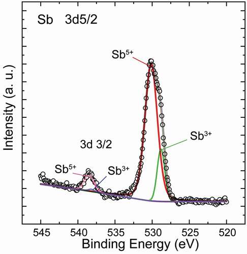
To clarify the oxidation state of Sb in the samples, XPS data was collected typically for x = 0.04 and is plotted within a local binding energy range for Sb 3d3/2 and 3d5/2 in . According to the peak processing, the asymmetric main peak is composed of the characteristic profiles for both Sb5+ (at 530.14 and 538.48 eV) and Sb3+ (at 528.82 and 538.2 eV). In addition, the former’s intensity is much stronger than the latter’s, indicating a higher proportion of 5+ states than the co-existing 3+ states. Based on charge balance, it is safe to assume the signal of Sb3+ should be from the Cu3SbS3 phase as an impurity. However, the appearance of weak Sb3+ signal, despite the absence of Cu3SbS3 peak in XRD pattern in the x = 0.04 sample, suggests that the Sb doped into the CTS phase should be in a mixed state where Sb5+ should be dominant relative to Sb3+. Therefore, it would be reasonable to deduce that the Sb should have acted as a donor when substituting the Sn4+ sites or Cu+ sites, which can be also supported by the electrical transport properties as follows.
Figure 5. XPS profile for the x = 0.04 sample, where the main peak can be decomposed into profiles for the co-existing 5+ and 3+ states. The much stronger intensity of the former indicates the 5+ state should be dominant as a whole
As one can see in ), the σ values for the Cu2Sn0.8-xSbxCo0.2S3 (x = 0, 0.02, 0.04, 0.06 and 0.08) samples all decrease as temperature rises, and the slope of the log σ vs log T relation is about −1 for all. Since the carrier concentration should be almost constant in such highly degenerate CTS materials, as has been verified in the Zn-doped CTS [Citation17], this means a same temperature dependence of carrier mobility and the carriers are predominantly scattered by acoustic phonons in all sample. Moreover, the σ for the Sb-substituted samples drops effectively with increasing x, from about 1320 S cm−1 for the merely Co-doped one to ~560 S cm−1 for the x = 0.08 one at 323 K, and the large discrepancy is even retained at 773 K. To verify the reason for the strong reduction of σ upon Sb substitution, Hall effect measurement for the carrier concentration n and Hall mobility µHall was conducted. Results (in ) showed a stepped reduction of n by ~1.7 × 1020 cm−3 corresponding to every increase of 0.02 at% Sb with x = 0 ~ 0.06, which is close to the estimated electron density, ~1.3 × 1020 cm−3, based on the assumption of fully ionized Sb5+ substituting for Sn4+, and the larger reduction in the determined n is possibly caused by the substitution of Sb for other atoms (Cu and Co), which would create more electrons to compensate for holes. The unexpected increase of n with x increasing from 0.06 to 0.08 is considered to be caused possibly by the increased formation of Cu vacancies. A possible reason may be linked with the effect of the secondary phase Cu3SbS3, since, according to the chemical composition, the formation of one Cu3SbS3 molecule always companies the generation of a Cu vacancy in Cu2SnS3, which can cause an increase of carrier concentration and a decrease in carrier mobility due to impurity scattering at the same time.
Table 2. Carrier concentration n, mobility µHall determined by Hall effect measurements and effective mass of carriers m* at 300 K estimated based on SPB model for Cu2Sn0.8-xSbxCo0.2S3 (x = 0, 0.02, 0.04, 0.06 and 0.08) samples
Figure 6. Thermoelectric properties of (a) electrical conductivity, (b) Seebeck coefficient and (c) power factor for the Cu2Sn0.8-xSbxCo0.2S3 (x = 0, 0.02, 0.04, 0.06 and 0.08) samples as a function of temperature. (d) the Pisarenko plot of S vs n at 300 K for the samples
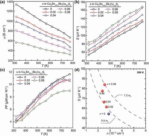
Besides, the mobility µHall is comparable to that in Zn [Citation24] or In-doped CTS [Citation30], and decreases abnormally with decreasing n as Sb content increases. This indicates the intensified carrier scattering due to factors other than carrier interactions, which could be related with the decreasing fraction of c-CTS that has a higher σ than t-CTS [Citation35].
Accordingly, the S values are enhanced as a result of the reduced n due to Sb doping, from ~54 μV K−1 for the x = 0 sample at 323 K to ~84 μV K−1 for the x = 0.08 one (see )). The steady increase of S with temperature suggests no bi-polaron effect has occurred and the compensation for holes by electrons due to Sb doping is stable in the present temperature range. In order to clarify the mechanism for the enhancement of S, a Pisarenko plot (i.e. S vs n) for all the Cu2Sn0.8-xSbxCo0.2S3 (x = 0, 0.02, 0.04, 0.06 and 0.08) samples was demonstrated in ), where 2 dashed lines with constant carrier effective mass, m*, estimated according to the single parabolic band (SPB) model relation of for the case of carriers being scattered dominantly by acoustic phonons [Citation38]. As can be seen, the m* increased gradually with increasing amount of Sb from ~5.5 mo to ~7.3 mo. As reported previously, a larger n is usually accompanied with the decrease in the Fermi level down in the VB, and this would cause an increase in m* due to the involvement of non-converged sub-bands located at deeper energy levels, even causing invalidity of SPB model in CTS-like compounds with complex band structures for deviation from parabolicity of the bands near the Fermi level. It should be noted that the Sb doping has caused the reduction of n, i.e. the elevation of Fermi level, which should have brought about a decrease rather than an increase in m*. However, the experimental data showed an opposite trend. A possible reason for this anomaly might be related to the electronic contribution from Sb 5s and 5p states with the Cu-3d orbitals in the valence bands. Actually, a similar effect has been clarified in CuSbS2 [Citation39], which would cause a net increase of density-of-states (DOS) near the Fermi level when the lone pair electrons first interact with S 3p electrons and the full antibonding orbital of this interaction is then sufficiently high so that it can subsequently interact with empty Sb 5p states, resulting in bonding states in the valence band and antibonding states at the bottom of the conduction band.
As a result, the power factors (PF = S2σ) in these Cu2Sn0.8-xSbxCo0.2S3 (x = 0, 0.02, 0.04, 0.06 and 0.08) samples are almost maintained, as shown in ), except for a slight drop at 773 K. It should be noted that these PFs (~10.4 μW cm−1 K−2 at 723 ~ 773 K) are still quite high as compared with that reported in the literature [Citation19,Citation24,Citation25,Citation28–30] so far for Cu2SnS3-based materials, and moreover, they are achieved by effective reduction of σ and simultaneous enhancement of S, which greatly suppresses the electronic thermal conductivity κe and consequently the total κ.
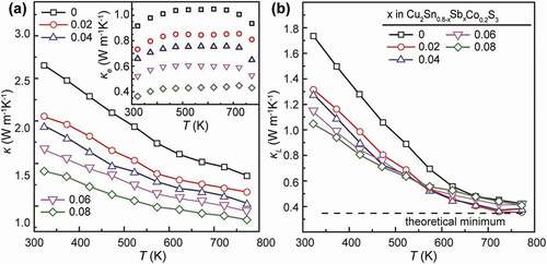
shows the thermal conductivities (κ, κe and κl) for Cu2Sn0.8-xSbxCo0.2S3 (x = 0, 0.02, 0.04, 0.06 and 0.08) samples. One can see in ) that the total κ for the x = 0 sample falls in a high range between 2.7 W m−1 K−1 and 1.7 W m−1 K−1 at 323 and 773 K, respectively. With an increase in Sb amount, the κ value is reduced significantly to 1.7 W m−1 K−1 and 0.88 W m−1 K−1. In the total κ, the κe values as a component are calculated from the relation, κe = LσT, where L is the Lorenz number estimated using the formula L = 0.5 + exp(S/116) [Citation40]. Thanks to the large reduction in σ, the κe values, as shown in the inset of ), are decreased drastically by almost 60 ~ 70%, from 0.9 ~ 1.05 W m−1 K−1 for the x = 0 sample in the temperature range of 323 ~ 773 K to 0.35 ~ 0.45 W m−1 K−1 for the x = 0.08 sample. Moreover, the lattice component, κl, is found to decrease gradually with x, optimally to 1.05 W m−1 K−1 at 323 K with x = 0.08 (in )). This can be related to the improved phonon scattering due to the alloying effect with enhanced mass-fluctuation as well as the presence of Cu3SbS3, which also exhibits very low κl of 0.2 ~ 0.3 W m−1 K−1 at 300 ~ 623 K [Citation41] with a high lattice vibrational anharmonicity due to the 5s2 orbital lone-pair electrons of the trivalent Sb atoms. As temperature rises up to 673 K, the κl values converge gradually to 0.3 ~ 0.4 W m−1 K−1 in the x = 0 sample. The ultralow κl in CTS has been reported frequently, and can be caused by the complex microstructure with disordered cation arrangement, which can also be referred to other materials like TmAlB4 [Citation42]. The convergence of κl at high temperatures indicates the predominant role of the cation-disordered feature on phonon transport interruption.
Figure 7. Thermal conductivities (κ, κe and κl) for all the Cu2Sn0.8-xSbxCo0.2S3 (x = 0, 0.02, 0.04, 0.06 and 0.08) samples. The dash line in (b) indicates a theoretical minimum of κl = 0.3 W m−1 K−1 at high temperatures
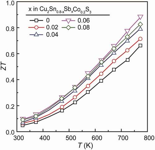
Finally, the ZT value calculated using the obtained parameters are plotted in . The x = 0 sample showed a maximal value of 0.65 at 773 K, which is smaller than the previous one [Citation20], due to the higher κe in the present sample which was sintered at a higher temperature for improved density. Thanks to the maintained PF and the suppressed κe and κ after Sb substitution, the ZT values are improved effectively to about 0.88. We also compared the data of Cu2Sn0.74Co0.2Sb0.06S3 with other Cu-Sn-S ternary compounds in , including Cu3SnS4- [Citation43], Cu7Sn3S10- [Citation44,Citation45] and Cu7Sn4S16- [Citation46], Cu5Sn2S7- [Citation37] based materials, indicating a prominent performance of our samples especially for the electrical transport properties.
Table 3. Electrical conductivity, Seebeck coefficient, power factor, thermal conductivity, lattice thermal conductivity, ZT and temperature for several high performance Cu-Sn-S TE materials at high temperature, including Cu3SnS4- [Citation43], Cu7Sn3S10- [Citation44,Citation45], Cu4Sn7S16- [Citation46], Cu5Sn2S7- [Citation37] based materials and Cu2Sn0.74Co0.2Sb0.06S3 in this work
Figure 8. ZT values vs temperature for Cu2Sn0.8-xSbxCo0.2S3 (x = 0, 0.02, 0.04, 0.06 and 0.08) samples. The peak value of 0.88 was obtained in the x = 0.06 sample at 773 K, which is 35% larger than that of x = 0 one, and is among the tops for CTS-based TE materials so far
4. Summary
The findings in this work demonstrate that, Sb-doping in the Co-doped CTS, can induce phase transformation from cubic to tetragonal structure, and serve as a donor and be used to tailor the hole concentration by charge compensation and incorporate the extra states of Sb in the VB, leading to a proper reduction of hole concentration while m* is enhanced. This gives rise to a maintained high PF of around 10.5 μW cm−1 K−2 at ~773 K and a simultaneously reduced κe. In addition, κl was further reduced due to the alloying effect and maintained at a low level of 0.3 ~ 0.4 W m−1 K−1 at ~723 K as a result of the lattice vibration nature of highly cation-disordered CTS. As a result, a high ZT of 0.88 has been realized at 773 K in the x = 0.06 sample (Cu2Sn0.74Sb0.06Co0.2S3), which stands among the tops so far of the CTS-based diamond-like ternary sulfides. Moreover, the preferential change in t-CTS component due to Sb doping suggests the possibility of further tailoring crystal chemistry, microstructural and electronic transport in the polymorphic CTS bulk by appropriate doping.
Acknowledgments
This research is supported by the National Natural Science Foundation of China under Grant No. 51672127, China Key National R&D Plan (No. 2017YFA0700705), and the Priority Academic Program Development of Jiangsu Higher Education Institutions (PAPD). We are grateful to the High Performance Computing Center of Nanjing Tech University for supporting the computational resources.
Disclosure statement
No potential conflict of interest was reported by the author(s).
Additional information
Funding
References
- Bell LE. Cooling, heating, generating power, and recovering waste heat with thermoelectric systems. Science. 2008 Sep;321(5895):1457–1461.
- Pei YZ, Wang H, Snyder GJ. Band engineering of thermoelectric materials. Adv Mater. 2012 Dec;24(46):6125–6135.
- Yang RG, Chen G, Kumar AR, et al. Transient cooling of thermoelectric coolers and its applications for microdevices. Energ Convers Manage. 2005 Jun;46(9–10):1407–1421.
- DiSalvo FJ. Thermoelectric cooling and power generation. Science. 1999 Jul;285(5428):703–706.
- Tritt TM, Subramanian MA. Thermoelectric materials, phenomena, and applications: a bird’s eye view. MRS Bul. 2006 Mar; 31(3):188–194.
- Search HCA, Iopscience M. Materials for thermoelectric energy conversion. Rep Prog Phys. 1988;51(4):459–539.
- Ang R, Khan AU, Tsujii N, et al. Thermoelectricity generation and electron-magnon scattering in a natural chalcopyrite mineral from a deep-sea hydrothermal vent. Angew Chem Int Ed. 2015 Oct;54(44):12909–12913.
- Takaki H, Kobayashi K, Shimono M, et al. Thermoelectric properties of a magnetic semiconductor CuFeS2. Mater Today Phys. 2017 Dec;3:85–92.
- Skoug EJ, Cain JD, Morelli DT. Thermoelectric properties of the Cu2SnSe3-Cu2GeSe3 solid solution. J Alloys Compd. 2010 Sep;506(1):18–21.
- Skoug EJ, Cain JD, Morelli DT. High thermoelectric figure of merit in the Cu3SbSe4-Cu3SbS4 solid solution. Appl Phys Lett. 2011 Jun;98(26):3.
- Parker D, May AF, Wang H, et al. Electronic and thermoelectric properties of CoSbS and FeSbS. Phys Rev B. 2013 Oct;88(15):1.
- Guelou G, Failamani F, Sauerschnig P, et al. Role of excess tellurium on the electrical and thermal properties in Te-doped paracostibite. J Mater Chem C. 2020 Feb;8(5):1811–1818.
- Khan AU, Al Orabi RA, Pakdel A, et al. Sb doping of metallic CuCr2S4 as a route to highly improved thermoelectric properties. Chem Mater. 2017 Apr;29(7):2988–2996.
- Berthebaud D, Lebedev OI, Maignan A, et al. Magnetothermopower and giant magnetoresistance in the spin-glass CuCrTiS4 thiospinel. J Appl Phys. 2018;124:6.
- Bourges C, Srinivasan B, Fontaine B, et al. Tailoring the thermoelectric and structural properties of Cu-Sn based thiospinel compounds CuM1+xSn1-xS4 (M = Ti, V, Cr, Co). J Mater Chem C. 2020 Dec;8(46):17.
- Xi L, Zhang YB, Shi XY, et al. Chemical bonding, conductive network, and thermoelectric performance of the ternary semiconductors Cu2SnX3 (X = Se, S) from first principles. Phys Rev B. 2012 Oct;86(15):14.
- Shen YW, Li C, Huang R, et al. Eco-friendly p-type Cu2SnS3 thermoelectric material: crystal structure and transport properties. Sci Rep. 2016;6:8.
- Zhao L, Chen CC, Pan L, et al. Magnetic iron doping in Cu2SnS3 ceramics for enhanced thermoelectric transport properties. J Appl Phys. 2019;125:9.
- Guélou G, Lemoine P, Raveau B, et al. Recent developments in high-performance thermoelectric sulphides: an overview of the promising synthetic colusites. J Mater Chem C. 2021;9:773–795.
- Suekuni K, Kim FS, Nishiate H, et al. High-performance thermoelectric minerals: colusites Cu26V2M6S32 (M = Ge, Sn). Appl Phys Lett. 2014 Sep;105(13):4.
- Zhang Z, Zhao H, Wang Y, et al. Role of crystal transformation on the enhanced thermoelectric performance in Mn-doped Cu2SnS3. J Alloys Compd. 2019;780:618–625.
- Berg DM, Djemour R, Gutay L, et al. Raman analysis of monoclinic Cu2SnS3 thin films. Appl Phys Lett. 2012;100:19.
- Oliva F, Arques L, Acebo L, et al. Characterization of Cu2SnS3 polymorphism and its impact on optoelectronic properties. J Mater Chem A. 2017 Dec 7;5(45):23863–23871.
- Zawadzki P, Baranowski LL, Peng H, et al. Evaluation of photovoltaic materials within the Cu-Sn-S family. Appl Phys Lett. 2013 Dec;103:25.
- Nguyen HTT, Zakhvalinskii VS, Pham TT, et al. Structural properties and variable-range hopping conductivity of Cu2SnS3. Mater Res Express. 2019 May;6(5):10.
- Onoda M, Chen XA, Sato A, et al. Crystal structure and twinning of monoclinic Cu2SnS3. Mater Res Bull. 2000 Jul;35(9):1563–1570.
- Chen XA, Wada H, Sato A, et al. Synthesis, electrical conductivity, and crystal structure of Cu4Sn7S16 and structure refinement of Cu2SnS3. J Solid State Chem. 1998 Aug;139(1):144–151.
- Xu X, Zhao H, Hu X, et al. Synergistic role of Ni-doping in electrical and phonon transport properties of Cu2Sn1-xNixS3. J Alloys Compd. 2017;728:701–708.
- Deng TT, Qiu PF, Song QF, et al. Thermoelectric properties of non-stoichiometric Cu2+xSn1-xS3 compounds. J Appl Phys. 2019 Aug;126(8):9.
- Tan Q, Sun W, Li ZL, et al. Enhanced thermoelectric properties of earth-abundant Cu2SnS3 via in doping effect. J Alloys Compd. 2016 Jul;672:558–563.
- Lohani K, Nautiyal H, Ataollahi N, et al. Experimental and Ab initio study of Cu2SnS3 (CTS) polymorphs for thermoelectric applications. J Phys Chem C. 2021 Jan;125(1):178–188.
- Zhao HW, Xu XX, Li C, et al. Cobalt-doping in Cu2SnS3: enhanced thermoelectric performance by synergy of phase transition and band structure modification. J Mater Chem A. 2017 Nov;5(44):23267–23275.
- Callaway J, Von Baeyer HC. Effect of point imperfections on lattice thermal conductivity. Phys Rev. 1960;120(4):1149–1154.
- Doebelin N, Kleeberg R. Profex: a graphical user interface for the Rietveld refinement program BGMN. J Appl Crystallogr. 2015 Oct;48:1573–1580.
- Li C, Shen YW, Huang R, et al. Hierarchically structured thermoelectric materials in quaternary system Cu-Zn-Sn-S featuring a mosaic-type nanostructure. ACS Appl Nano Mater. 2018 Jun;1(6):2579–2588.
- Li C, Song HL, Shen YW, et al. Evolution of cation ordering and crystal defects controlled by Zn substitutions in Cu2SnS3 ceramics. Aip Adv. 2018;8:10.
- Kumar VP, Lemoine P, Carnevali V, et al. Ordered sphalerite derivative Cu5Sn2S7: a degenerate semiconductor with high carrier mobility in the Cu-Sn-S diagram. J Mater Chem A. 2021. DOI:https://doi.org/10.1039/D1TA01615F
- Snyder GJ, Toberer ES. Complex thermoelectric materials. Nat Mater. 2008 Feb;7(2):105–114.
- Whittles TJ, Veal TD, Savory CN, et al. Core levels, band alignments, and valence-band states in CuSbS2 for solar cell applications. ACS Appl Mater Interfaces. 2017 Dec;9(48):41916–41926.
- Kim HS, Gibbs ZM, Tang YL, et al. Characterization of Lorenz number with Seebeck coefficient measurement. Apl Mater. 2015 Apr;3(4):5 .
- Du BL, Zhang RZ, Liu M, et al. Crystal structure and improved thermoelectric performance of iron stabilized cubic Cu3SbS3 compound. J Mater Chem C. 2019 Jan;7(2):394–404.
- Wang XJ, Mori T, Kuzmych-Ianchuk I, et al. Thermal conductivity of layered borides: the effect of building defects on the thermal conductivity of TmAlB4 and the anisotropic thermal conductivity of AlB2. APL Mater. 2014;2:4.
- Yang YB, Ying PZ, Wang JZ, et al. Enhancing the thermoelectric performance of Cu3SnS4-based solid solutions through coordination of the Seebeck coefficient and carrier concentration. J Mater Chem A. 2017 Sep 21;5(35):18808–18815.
- Deng TT, Xing T, Brod MK, et al. Discovery of high-performance thermoelectric copper chalcogenide using modified diffusion-couple high-throughput synthesis and automated histogram analysis technique. Energ Environ Sci. 2020 Sep 1;13(9):3041–3053.
- Deng T, Qiu P, Xing T, et al. A low-cost and eco-friendly Br-doped Cu7Sn3S10 thermoelectric compound with ZT around unity. J Mater Chem A. 2021 Feb;9(12):7946–7954.
- Cui JL, He TT, Han ZK, et al. Improved thermoelectric performance of solid solution Cu4Sn7.5S16 through isoelectronic substitution of Se for S. Sci Rep-Uk. 2018;29:8.