
 ?Mathematical formulae have been encoded as MathML and are displayed in this HTML version using MathJax in order to improve their display. Uncheck the box to turn MathJax off. This feature requires Javascript. Click on a formula to zoom.
ABSTRACT
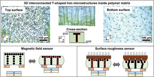
The fillers inside a polymer matrix should typically be self-assembled in both the horizontal and vertical directions to obtain 3-dimentional (3D) percolation pathways, whereby the fields of application can be expanded and the properties of organic-inorganic composite films improved. Conventional dielectrophoresis techniques can typically only drive fillers to self-assemble in only one direction. We have devised a one-step dielectrophoresis-driven approach that effectively induces fillers self-assembly along two orthogonal axes, which results in the formation of 3D interconnected T-shaped iron microstructures (3D-T CIP) inside a polymer matrix. This approach to carbonyl iron powder (CIP) embedded in a polymer matrix results in a linear structure along the thickness direction and a network structure on the top surface of the film. The fillers in the polymer were controlled to achieve orthogonal bidirectional self-assembly using an external alternating current (AC) electric field and a non-contact technique that did not lead to electrical breakdown. The process of 3D-T CIP formation was observed in real time using in situ observation methods with optical microscopy, and the quantity and quality of self-assembly were characterized using statistical and fractal analysis. The process of fillers self-assembly along the direction perpendicular to the electric field was explained by finite element analogue simulations, and the results indicated that the insulating polyethylene terephthalate (PET) film between the electrode and the CIP/prepolymer suspension was the key to the formation of the 3D-T CIP. In contrast to the traditional two-step method of fabricating sandwich-structured film, the fabricated 3D-T CIP film with 3D electrically conductive pathways can be applied as magnetic field sensor.
GRAPHICAL ABSTRACT
IMPACT STATEMENT
A one-step electric field-induced self-assembly method was developed to efficiently control the self-assembly of fillers along two orthogonal axes to form three-dimensional interconnected T-shaped microstructure assembles of carbonyl iron powder inside a polymer matrix.
1. Introduction
Organic-inorganic hybrid materials are a type of functional composite material prepared by the introduction of inorganic fillers with enhanced properties into a polymer matrix [Citation1]. The composites can be designed to enhance the mechanical properties and produce additional properties such as electrical and thermal conductivity while maintaining the soft, lightweight, and chemical resistance properties of the polymer matrix [Citation2,Citation3]. Conventional composites are prepared for simple single-directional enhancement of the properties and have limited fields of application [Citation4–6]. The application of new functional materials with enhancement of the three-dimensional (3D) multi-directional properties has recently been expanded to the fields of sensors, electromagnetic shielding, thermal management, and energy storage [Citation7–11].
According to percolation theory, isotropic composites formed by simply mixing a filler and matrix often require a high-volume fraction of filler that is above the percolation threshold to effectively form 3D percolation pathways whereby significant enhancement of the 3D multi-directional properties can be achieved [Citation12]. For example, the thermal conductivity of 40 w% boron nitride (BN) nanosheets/Epoxy, 10 wt% graphene/polypropylene (PP), and 27.1 vol% ZnO/polyimide isotropic composites were improved with this approach by 26-, 6.5-, and 4.1-fold, respectively [Citation13–15]. However, the simultaneous addition of an excess of filler typically has agglomeration problems due to inhomogeneous dispersion, reduces the mechanical properties and transparency of the composites, and increases the manufacturing costs [Citation16]. Therefore, the achievement of a very high level of multi-directional performance enhancement with the addition of only a very small amount of filler to maintain the properties of the polymer matrix is necessary for the preparation of novel multifunctional composite materials [Citation17].
More attention has recently been paid to the construction of 3D interconnected microstructures of fillers in polymer matrix, which can maximize the formation of effective 3D percolation networks by a reduction of filler-filler interfacial hindrances to achieve high performance enhancement with a small filler content. Many novel methods, including the chemical vapor deposition method [Citation18], protein foaming technique [Citation19], electroless plating method [Citation20] and template method [Citation21,Citation22], have been applied to the construction of 3D interconnected microstructures. However, these methods tend to be particularly complex and high cost, which significantly limits large-scale production and the fields of application.
Our previous studies [Citation23,Citation24] and those of others [Citation25,Citation26] have employed a simple self-assembly approach to successfully construct one-dimensional (1D) interconnected microstructures of fillers within polymer matrix. The application of an external force to drive the motion and orientation of the internal fillers in a polymer precursor allows for control of the internal fillers to self-assemble into percolation pathways, which results in highly enhanced electrical and thermal conductivity performance, even with only small amounts of filler. For film-like composites, the internal filler has typically been controlled to self-assemble along the surface or thickness direction of the film to form percolation pathways with a very small amount of filler. Hu et al. [Citation27] used shear force to align silver nanowires on the surface of a matrix to obtain high electrically conductive transparent films. Lin et al. [Citation28] used magnetic field to assemble BN nanosheets in the thickness direction for high thermal conductivity films. However, these methods can only achieve self-assembly in a single direction along the driving force and cannot result in 3D percolation networks that are assembled along multiple directions. Methods to apply multiple external forces in different directions tend to be relatively complex, and the filler will typically be assembled along a single direction of the combined force rather than in multiple directions independent of each other [Citation29]. Therefore, it remains a challenge to simultaneously control the self-assembly of filler materials in multiple directions during one step.
In this study, we have developed a simple one-step self-assembly method to successfully fabricate iron/polymer composites with three-dimensional interconnected T-shaped iron microstructures (3D-T CIP) with very small amounts of filler (0.2–2 vol%). An external alternating current (AC) electric field and a non-contact technique were used to control the self-assembly of carbonyl iron powder (CIP) in a polymer. Firstly, the formation process of the 3D-T CIP was observed using an in situ observation system, and the degree of self-assembly of the surface network structure was then assessed by statistical and fractal analyses. The self-assembly process at the surface was explained by numerical simulations, and the electrical properties of the fabricated 3D-T CIP films were finally evaluated and applied to magnetic field sensor.
2. Experimental details
2.1. Materials
Carbonyl iron powder (CIP) with an average particle diameter of 5–9 μm and a resistivity of 9.71 μΩ·cm (Sigma-Aldrich Japan, cat. no. 44890) were used as-received without surface treatment (see the scanning electron microscope image of CIP in Figure S1). An insulating polymer matrix was formed by the polymerization reaction of a liquid polysiloxane precursor (Shin-Etsu Chemical Japan, KE-103; viscosity: 1 Pa·s, volume resistivity: 0.8 TΩ·m, relative permittivity: 3.1) and a curing agent (Shin-Etsu Chemical Japan, CAT-103) in a mixing ratio of 20:1.
2.2. Sample preparation
The CIP/polysiloxane prepolymer suspension was prepared as shown in , where different amounts of CIP (0.2–2 vol%) were weighed and mixed in a container with the KE-103 polysiloxane prepolymer, and the suspension was then stirred at 1800 rpm for 15 min using a high-speed mixer (Uni-Cyclone UM-103S, Japan Unix). The CAT-103 curing agent was then added to the suspension at a mixing ratio of 20:1 and stirred at 1800 rpm for 5 min until a homogeneous distribution was achieved. The resultant suspension was then immediately placed into a mold (18 mm × 18 mm × 220 µm) for self-assembly treatment before the suspension was cured.
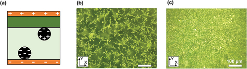
Figure 1. Schematic illustration of CIP/polymer composite film fabrication process; (a) fabrication of CIP/prepolymer suspension, (b) electric field treatment method with EISE system, and (c) two-step sandwich method as control group. (d) Schematic illustration of real-time in situ observation (bright-field illumination) of the movement of CIPs from (d-1) the top and bottom surfaces, and (d-2) the side view. (e) Schematic illustration of the fabricated composite film observation (dark-field illumination).
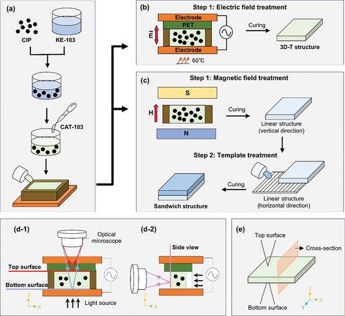
As shown in , the CIP/prepolymer suspension was placed in a uniform AC electric field in the vertical direction for the electric field-induced self-assembly treatment. The AC electric field was generated between two indium tin oxide (ITO)-coated glass electrodes from an AC power supply (WT-8752, Hioki E.E.) with an output voltage of 50 V-5 kV (50 Hz). An insulating film, such as polyethylene terephthalate (PET) film with a thickness of 75 μm or a high-voltage-resistant polyimide film, was added between the top electrode and the suspension (considering the effect of gravity, the film was fabricated with the PET film at the bottom side as shown in Figure S2(b-1)). The entire system from top to bottom formed a sandwich shape of electrode-insulator-suspension-electrode (EISE). After the electric field induced treatment at 60°C for 15 min, the suspension was almost solidified, and the specimens were then finally transferred to a thermostatic drying oven at 80°C for 1 h to complete the curing process.
As a control experiment, composites film with 3D internal self-assembled CIP microstructures was also fabricated using a two-step sandwich method (). In the first step, a vertically self-assembled layer was fabricated using the applied magnetic field induction method, and then in the second step, a horizontally self-assembled layer was superimposed on top of the first layer using the template method to form a sandwich-structured film. (Refer to the supplementary document of the fabrication of the sandwich-structured film.)
2.3. Sample characterization
2.3.1. Observation of structures
A real-time in situ observation system () was used to observe the self-assembly of CIP on the top and bottom surfaces () and in the thickness direction ()). The samples were placed between an optical microscope (VHX-9000, Keyence) with a magnification of 500× and an LED light source, where the LED light could penetrate the EISE system into the microscope due to the good transmittance of the various layers in the EISE system, i.e. the ITO glass electrodes, the PET insulating film, and the suspension with a low amount of filler (0.2–2 vol%). The mechanism for the motion of CIPs in the prepolymer matrix was evaluated by in situ observation and finite element method simulation (COMSOL Multiphysics (version 5.4)). After the polymer had completely cured into a film (), the internal CIP structure of the fabricated composite film was observed using optical microscopy with dark-field illumination (bright-field illumination for in situ observation).
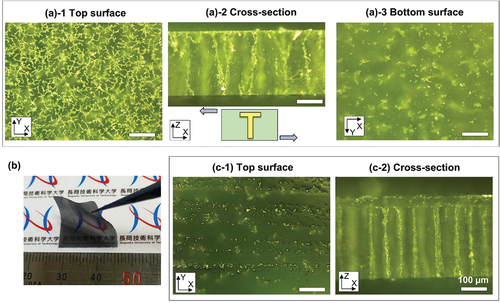
Figure 2. (a-1) Top surface, (a-2) cross-section, (a-3) bottom surface micrographs, and (b) physical image of 2 vol% CIP/polymer composite film treated under AC electric field (0.5 kV/mm) for 15 min. (c-1) top surface, (c-2) cross-section microscopic image of 2 vol% CIP/polymer sandwich-structured film: the top layer was fabricated using the template method for self-assembly in the surface direction, and the bottom layer was fabricated using the magnetic field-induced method for self-assembly in the thickness direction.
2.3.2. Analysis of images
Optical microscopy images were statistically and fractally analyzed using ImageJ software (version 1.53) [Citation30]. The images were first subjected to background enhancement, grayscaling, and thresholding treatment. The resulting binary image was then subjected to particle identification and differentiated from self-assembly based on the circularity of the particles calculated using the following equation [Citation30]:
where S and C represent the area and perimeter of the recognized particle, respectively. The circularity of a circle is 1. When multiple circles are connected to each other to form a chain, the value of circularity gradually becomes smaller as more circles form the chain. Considering that the 2D images of CIP particles have complex shapes, the particles with circularity lower than 0.33 in the images are regarded as self-assembled CIP aggregates. (When three circles are connected head to tail, the circularity is 0.33.)
The CIP area ratio parameter was introduced to characterize the proportion of the entire surface space occupied by all CIP particles at the surface:
The self-assembly ratio parameter was introduced to characterize the ratio of self-assembled CIP aggregates to all CIP particles in the image. The self-assembly ratio was calculated by:
where the statistical areas of all CIPs and isolated CIPs particles were calculated using the automatic particle analysis function of ImageJ software with macro processing. The self-assembly ratio is 0% when all CIPs are completely dispersed in the polymer matrix, and 100% when all CIPs are self-assembled.
The fractal dimension (D) was used to describe the geometrical complexity of the CIP self-assemblies. The contours of the CIP aggregates in the binarized images were extracted, and the box counting method was then used to count the number of different sized grids (boxes) occupied by the contours of the CIP aggregates [Citation31,Citation32]. The log values of the number of grids and the corresponding grid sizes were then calculated and plotted. Finally, linear regression was performed to obtain the slope to calculate the fractal dimension:
where N(r) and r represent the number of boxes covering the CIP aggregates and the size of the boxes, respectively. The boundaries of the aggregates composed of CIP in the 2D microscopic images have a fractal dimension between 1 and 2, where the larger values of fractal dimension indicate more complex boundaries.
The self-assembly ratio and the fractal dimension were used to characterize the quantity and quality of CIP self-assemblies, respectively.
2.3.3. Characterization of properties
The CIP/polymer composite films fabricated under different conditions were sandwiched between two copper electrodes and the current-voltage (I-V) characteristics were measured using a digital meter (Keithley 2400 source meter) and a DC power supply (Kikusui PMX350–0.2A). The contact area between the electrodes and the film was increased by rubbing the surface of the copper electrodes with sandpaper and applying a preload force of 3N. Due to the high resistance of the low concentration CIP/polymer composites, the current varied considerably after switching on the power supply and it was necessary to wait for 1 minute before taking measurements. For measurements of magnetic field response characteristics, the surface resistance of the fabricated film was measured by the two-point probe method at room temperature at a reference voltage of 100 V. The transmittance of the composites was measured using a ultraviolet-visible (UV-Vis) spectrophotometer (Jasco V650).
3. Results and discussion
3.1. Three-dimensional interconnected T-shaped iron microstructures
Microscopy observations of a 2 vol% CIP/polymer composite film treated under AC electric field (0.5 kV/mm) were taken from different views, as shown in and S2. The surface micrographs show different aggregation structures on the top and bottom surfaces of the composite film. The top surface view () shows the CIPs assembled with each other into two-dimensional interconnected network iron microstructures (2D-NW CIP) on the top surface of the composite film. However, the micrograph of the bottom surface () shows that the CIPs were evenly dispersed on the bottom surface without self-assembly, and the number of CIPs was significantly less than that on the top surface. And as shown in Figure S2, when the PET film was placed on the top, the number of CIPs on the no-PET side was increased under the effect of gravity, but the CIP content on the PET side was still higher than that on the no-PET side.
The cross-sectional view of the approximately 220 µm thick composite film () shows the CIPs clearly self-assembled into one-dimensional interconnected linear iron microstructures (1D-I CIP) along the thickness direction of the film, which connected the top and bottom surfaces of the composite film. At the same time, there was a very thin layer of CIPs at the top end of the cross-sectional view but not at the bottom end.
The structure formed in the composite film was termed a three-dimensional interconnected T-shaped iron microstructure (3D-T CIP), which resembles the letter ‘T’ when viewed from the side.
In previous reports, the filler could only be assembled along a single direction by the conventional self-assembly method, i.e. the surface or thickness direction of the film [Citation33–35]. As shown in and Figure S3, the traditional single-direction self-assembly method involves at least two steps to form the 3D sandwich-structured film. In the present method, the self-assembly of CIPs in both the film surface direction and film thickness direction was achieved in only one step. In comparison with the two-step sandwich-structured film, the present one-step method is simpler. Under the same fabrication conditions, the one-step 3D-T CIP film is thinner (), which increases the application field and reduces the fabrication cost. Moreover, as shown in Figure S3(d), in the sandwich-structured film, the separately fabricated CIP structures in the top and bottom layers were not matched, which affected the formation of the 3D percolation pathways. In contrast, the 3D-T CIP film had a continuous and tightly integrated 2D-NW CIP and 1D-I CIP, which enhanced the formation of 3D percolation pathways.
3.2. Kinematic mechanism of 3D orthogonal bidirectional self-assembly
The one-step 3D self-assembly method is referred to as orthogonal bidirectional assembly, which means that the CIPs are self-assembled simultaneously along the directions parallel (thickness direction) and perpendicular (surface direction) to the electric field. The formation of the 3D-T CIP structure can be considered as a combination of three actions, i.e. self-assembly along the vertical direction, aggregation on the top surface, and self-assembly along the horizontal direction.
3.2.1. Self-assembly in the parallel electric field direction and aggregation on the PET film surface
The motion of CIPs in the prepolymer under an applied electric field was observed using an in situ observation system. and Supplementary Video S1 show that under the action of the applied electric field, the dispersed CIPs moved at high speeds and assembled with each other over time. This is because fillers were induced to polarize by the applied electric field and assembled with each other under the action of the dipole – dipole interaction [Citation36,Citation37]. Finally, the CIPs assembled into one-dimensional interconnected I-shaped iron microstructures (1D-I CIP) along the direction of the electric field. After the 1D-I CIP was formed, the neighboring 1D-I CIP would be attracted to each other and combine to form a single 1D-I CIP. Therefore, the density of the 1D-I CIP can be controlled by controlling the application time of the electric field. For example, increasing the working temperature and using curing promotion agent to speed up the curing of the polymer.
Figure 3. 0.5 vol% CIP/prepolymer suspension under AC electric field (1 kV/mm) as a function of the application time; (a-1) 0 s, (a-2) 5 s, and (a-3) 20 s. (b) After applying the electric field for 300 s, (b-1) a large amount of CIP aggregates on the left insulator surface, (b-2) while no significant aggregation on the right electrode surface. Schematic illustration of the structure formed by CIP on the side view (from left to right: Electrode, Insulator, Suspension and Electrode).
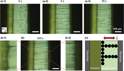
Extremely high electric fields are typically required to drive sub-micron sized filler particles due to the high viscosity of the liquid polysiloxane prepolymer. When linear conductive CIP pathways are formed between the electrodes, the resistance of the system is significantly reduced, which leads to electrical breakdown of the system at high voltage and low resistance [Citation38]. Therefore, a non-contact technique of adding an insulating film between the electrode and the suspension was used to prevent electrical breakdown of the system.
shows that after the applied electric field treatment, many CIPs were aggregated near the surface of the insulator film, but no CIP aggregation was observed at the side that was in direct contact with the electrode. After the AC electric field treatment, the 3D-T CIP was formed, as shown in .
As shown in , on the side without the insulator PET film, contact charge electrophoresis [Citation39] occurs once the CIP in contact with the electrode. The uncharged CIPs are charged near the electrode, at which moment the CIP have the same charge sign as the electrode, which creates a repulsive force between the electrode and the charged CIP. But on the side with the PET film, the CIPs were blocked by the PET film when they approached the electrode and could not continue to approach the electrode.
Figure 4. (a) Schematic illustration of CIP charging in contact with the bottom electrode and not charging on the top PET surface. Top surface micrograph of 2 vol% CIP/polymer composite film treated under (b) 0.3 kV/mm AC electric field and (c) 2 kV/mm DC electric field for 15 min.
In our previous study [Citation40], two insulating PET films were placed at both the top and bottom sides and an 3D H-shaped structure was successfully fabricated. However, compared with the EISE system, PET films at both sides caused the CIPs to lose the opportunity of contact charging, and thus a higher electric field and a relatively high CIP concentration were required to drive the CIPs to self-assembly. As shown in , the CIP in the EISE system can still be self-assembled at a very low electric field of 0.3 kV/mm.
As shown in , when a DC electric field was applied to the EISE system, the charged CIP in contact with the bottom electrode would move towards the upper PET film by the electrophoresis, resulting in a large amount of CIP aggregating on the top PET surface. In contrast, when an AC electric field was used, since the direction of the electric field was changing alternately, the electrophoresis resulted in oscillatory movement of the CIP near the equilibrium position, and the instantaneous aggregation of a large number of CIPs on the surface of the top PET film did not occur. Therefore, it is possible to control the amount of CIP aggregation on the top PET surface by switching the use of AC electric field and DC electric field.
3.2.2. Self-assembly in the vertical electric field direction
The movement of CIP on the surface was observed using the real-time in situ observation system, and the results are shown in . Initially, the well-stirred CIP particles were randomly and uniformly distributed in the suspension, and few large aggregates of CIPs were evident in the surface view (-1)). After application of the external AC electric field, the CIPs distributed in the surface layer rapidly aggregated and interconnected on the lower surface of the PET film within several seconds and formed radial structures (2)). When most of the CIPs on the surface formed radial structures, the center part of the radial structure was basically motionless, and the end of the radial structure still had a slight motion. The end of the radial structure then gradually absorbed the CIP particles that reached the surface from the bottom layer through electrophoresis, and the radial structure gradually spread. Finally, most of the CIPs on the surface were connected to each other to form 2D-NW CIP.
Figure 5. Optical micrograph of the surface (with PET side) of a 0.5 vol% CIP/prepolymer suspension under AC electric field (2 kV/mm) treatment for (a-1) 0 min, (a-2) 1 min, and (a-3) 5 min. Results of statistical and fractal analyses of images obtained from in situ observations: (b) CIP self-assembly ratio and area ratio as a function of time. (c) Plot of the relationship between the number of boxes and box size obtained by the box counting method. (d) Fractal dimension as a function of time.
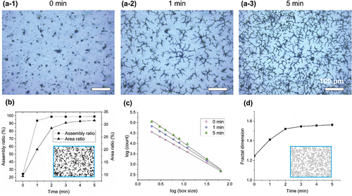
The process of CIP self-assembly on the top surface was evaluated by statistical and fractal analyses. The degree of assembly of CIPs on the surface was statistically calculated by calculation of the self-assembly ratio using EquationEquation (3)(3)
(3) . As shown in , the self-assembly ratio was 24.52% when no electric field was applied, where most particles were independently dispersed, except for a small amount of CIP aggregation due to van der Waals forces and electrostatic forces. When the electric field was applied for 1 min, the CIPs rapidly aggregated and assembled, and the self-assembly ratio reached 93.63%, after which the increase of the self-assembly ratio slowed down. After 5 min of electric field application, 98.98% of the CIPs on the surface were self-assembled into a network structure. After application of the electric field, the CIPs that were uniformly dispersed in the suspension gradually moved through the contact charge electrophoresis action and finally aggregated on the top surface, and the percentage of the CIP area on the top surface increased from the initial 9.49% to 31.61% after 5 min. As shown in , the number of boxes occupied by the contours of the radial CIP network structure on the surface was counted using the box counting method and fitted using a linear function. The Y-intercept value of the fitted straight line increased gradually with the electric field application time, which was attributed to an increase of the aggregated CIPs on the surface and the corresponding increase in the number of boxes occupied by the CIP contours. The slope of the fitted straight line increased with time, which indicated an increase of the fractal dimension. The fractal dimension grew from the initial 1.25 to 1.56 at 5 min, as shown in , which indicates that the contour of the self-assembled CIP tends to be complex.
The mechanism for the motion of CIP self-assemblies on the top surface was explained using numerical simulation, as shown in . shows a 75 μm PET film layer and 220 μm polymer layer sandwiched between the top and bottom electrodes, where the potential in the polymer varies uniformly from the bottom electrode to the bottom surface of the PET when a bias voltage of 295 V is applied to the bottom electrode and the top electrode is kept grounded. However, when conductive CIP particles were added to the polymer, as shown in and the conductive CIP were assembled into a 1D-I CIP along the direction of the electric field, the potential was no longer varied uniformly. The insulated PET film was sandwiched between the top of the chain composed of conductive CIPs and the upper electrode. According to Ohm’s law for parallel circuits, the resistance of the insulating PET film is much greater than that of the conductive 1D-I CIP; therefore, the potential difference between the top and bottom ends of the 1D-I CIP will be much less than the potential difference between the top of the 1D-I CIP and the upper electrode. An inhomogeneous electric field will thus be generated around the top of the conductive 1D-I CIP.
Figure 6. Simulation of the potential change between flat plate electrodes: (a) uniform variation of potential in the absence of 1D-I CIP. (b) Uneven variation of potential at the top of the chain in the presence of a 1D-I CIP. (c) Simulation of the electric field strength between adjacent CIPs on the top surface. The electric field between CIPs is very small when two isolated CIPs are distributed adjacent to each other on the top surface. (d) When isolated CIPs are distributed adjacent to a 1D-I CIP on the top surface, the electric field between the CIPs is very large and the isolated CIP on the left is subjected to a horizontal rightward electric field force. (The Maxwell’s surface stress tensor is indicated by a white arrow.) Simulated environment: CIP (10 µm)/prepolymer suspension treated with an electric field of 1 kV/mm.
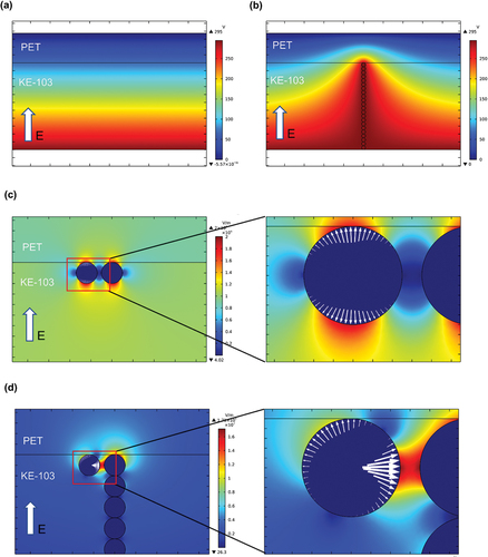
The electric field strength between adjacent CIPs on the top surface and the electric force acting on them were simulated using simulation software. As shown in , when two isolated CIP were distributed adjacent to each other on the top surface, the CIPs were polarized by the applied electric field, and the direction of polarization was along the direction of the electric field (in the vertical direction), with a very small degree of change in the electric field in the horizontal direction between the CIPs. Integration of the Maxwell surface stress tensor [Citation41] on the left CIP shows that the horizontal combined force on the left CIP exhibits a repulsive force of −7.73 × 10⁻² mN. The repulsive force between the CIPs drives the CIPs away from each other. When the isolated CIP was distributed adjacent to the 1D-I CIP on the top surface due to the field focusing effect [Citation42], as shown in , the electric field strength at the top part of the CIP chain was very high. The isolated CIP on the left was subjected to a horizontal polarization by the high potential at the top of the 1D-I CIP on the right. Integration of the Maxwell surface stress tensor on the left CIP shows that the horizontal combined force
on the left CIP exhibits an attractive force of 9.48 mN. The horizontal rightward electric field force acting on the left CIP drives the CIP closer to the top of the right 1D-I CIP, and the CIPs self-assemble in the horizontal direction.
The actuation force for CIP self-assembly on the top surface mirrors that of dielectric electrophoresis (DEP), which refers to the induced force on the dielectric filler in a non-uniform electric field [Citation43]. A spherical particle in a non-uniform electric field forms an induced dipole, which is subjected to a DEP force that is dependent on the electric field gradient:
where is the radius of the CIP,
is the permittivity of the polymer media surrounding the CIP, E is the root-mean-square value of the electric field, and Re[K(ω)] is the real part of the Clausius–Mossotti factor:
where the complex permittivity under an AC electric field is:
where is the conductivity and
is the angular frequency of the AC electric field. Therefore, the mechanism for the self-assembly of CIPs in the horizontal direction on the surface of PET film is that, firstly, under the action of the electric field in the vertical direction, the CIPs form 1D-I CIP along the vertical direction, and the electric field focusing effect at the top of the 1D-I CIP then generates a non-uniform electric field, and the surrounding adjacent CIPs come close to the 1D-I CIP to complete self-assembly under the action of dielectrophoresis.
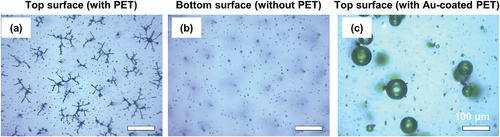
Control experiments were performed to further confirm that the insulating PET film between the 1D-I CIP and the top electrode is critical for the self-assembly of CIPs on the top surface. In contrast to the self-assembly of CIPs into a 2D-NW CIP on the top surface (), no self-assembly occurred on the bottom surface (). This is because there is no insulating PET film between the lower end of the 1D-I CIP and the electrode, and the potential of the lower end of the 1D-I CIP is the same as that of the directly-contacting electrode (as shown in the electric potential simulation in , and there is no generation of a horizontally-directed non-uniform electric field at the lower end of the 1D-I CIP. When the side of the insulating PET in contact with the suspension was treated with a gold (Au) coating (), the CIPs on the surface of the Au-coated PET layer also did not self-assemble. When the top of the 1D-I CIP was in contact with the high electrical conductivity Au layer, the potentials of the Au layer and the 1D-I CIP were the same, and therefore no horizontal dielectrophoresis occurred at the top of the 1D-I CIP.
Figure 7. Optical micrographs of the surface of a 0.2 vol% CIP/prepolymer suspension after AC electric field (2 kV/mm) treatment for 5 min. For the electrode/PET/suspension/electrode system, (a) the CIPs on the top surface (with PET layer) self-assembled into a network structure (b), there was no self-assembly on the bottom surface (without a PET layer), and for the electrode/Au-coated PET/suspension/electrode system (c), there was no self-assembly of the CIPs on the top surface (with a Au-coated PET layer), and insulation breakage occurred to produce many bubbles.
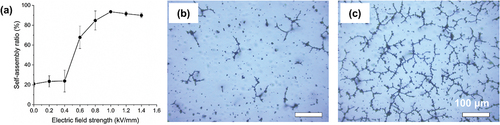
The degree to which the CIPs assemble into 2D-NW CIPs on the surface is dependent on the strength of the applied electric field. As shown in , when the electric field strength was lower than 0.4 kV/mm, dielectrophoresis was insufficient to overcome the resistance to drive the CIPs to self-assemble in the horizontal direction, and the self-assembly ratio of the CIPs was exceptionally low at 23.81%, which was almost the same as that of 20.92% when there was no electric field treatment. However, when the electric field strength was higher than a critical value, the self-assembly ratio increased rapidly and reached a maximum at an electric field strength of 1 kV/mm. In AC electric fields with the same frequency, the strength of the electric field is positively correlated with the electric field gradient, so that higher electric field generates higher dielectrophoretic force.
Figure 8. (a) Self-assembly ratio of a 0.2 vol% CIP/prepolymer suspension under AC electric field treatment for 5 min as a function of electric field strength. Optical micrographs for treatment with (b) 0.6 kV/mm and (c) 1 kV/mm.
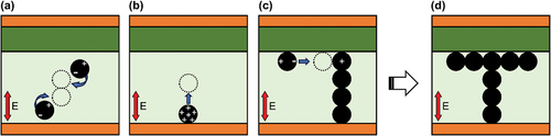
Therefore, as shown in , the mechanism for the formation of 3D-T CIPs can be summarized as a combination of three effects: (a) the electric field induces the polarization of CIP, and then adjacent CIPs assemble along the vertical direction under the action of the dipole moment; (b) some of the CIPs aggregate towards the upper PET film due to the effect of contact charge electrophoresis; (c) near the inhomogeneous electric field generated at the tip of the 1D-I CIP, the CIPs self-assemble along the horizontal direction by dielectrophoretic force.
Figure 9. Mechanism for the formation of 3D-T CIPs can be considered as a combination of three actions: (a) self-assembly along the vertical direction, (b) charge and aggregate on the top surface, and (c) self-assembly along the horizontal direction. (d) The resulting T-shaped structure.
3.3. Properties and applications
The electrical properties of the composites can be substantially enhanced by changing the internal CIP self-assembly structure. As shown in , the 3D-T CIP film formed after the orthogonal bidirectional self-assembly method shows good electrical conductivity. For the 2 vol% isotropic CIP/polymer film, the gaps between the CIPs hinder the current transmission and shows high electrical resistance. Without changing the filler amount, a more compact and continuous self-assembled structure was formed between the CIPs after the orthogonal bidirectional self-assembly treatment, resulting in compact conductive pathways for efficient current transfer. However, the electrical properties of the sandwich-structured film, although higher than the isotropic film, is much lower than that of the 3D-T CIP film. Because the 1D-I CIP structure between the upper and lower layers of the sandwich structure cannot be well articulated (Refer to and S3(d) for microscopic images of sandwich-structured film), there has a high resistance at the interface between the upper and lower layers, which reduces the overall electrical performance of the composite film. As shown in Figure S4, the one-layer 1D-I CIP structured film shows high electrical conductivity, but when two films are stacked on top of each other, the electrical conductivity is reduced drastically.
Figure 10. (a) The current-voltage (I-V) characteristics of 2 vol% CIP/polymer composite films treated by three different methods. Schematic diagrams were used to explain the electrical properties of 3D-T CIP (left) sandwich (middle) isotropic (right) composite films, respectively. (b) The ultraviolet-visible (UV-Vis) transmission spectrum of 2 vol% CIP/polymer composite films as a function of wavelength. And the inside photo shows that the lower pattern can be clearly seen through the 2 vol% 3D-T CIP composite film. (c-1) schematic illustration of the mechanism for a magnetic field sensing element and (c-2) surface resistance changes for a 2 vol% 3D-T CIP film as a function of the external magnetic field strength.
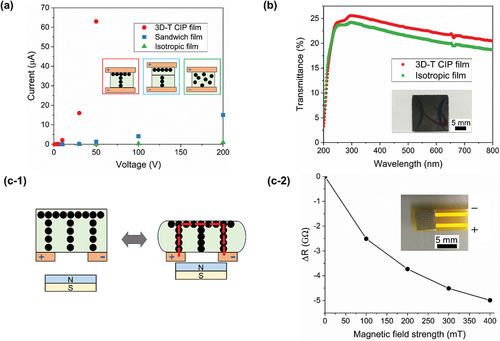
As shown in , the UV-Vis transmission spectra of the 2 vol% composite film show that the 3D-T CIP film maintains a good degree of transparency in the visible range at low filler content. Although many CIPs aggregated on the top surface reduces the transparency, the cross-section ()) shows that only a thin layer of CIPs aggregated on the surface. And the 1D-I CIP structure in the vertical direction greatly increases the visible light transmittance, and thus the transmittance of 3D-T CIP films is approximately the same as that of isotropic film. 3D-T CIP films have superior conductivity while maintaining high transmittance, which are promising for a wide range of applications, such as in 3D integration circuits, sensors, and water cleaning systems.
The 3D-T CIP films can be applied to magnetic field sensor, as shown in . A pair of swirl-shaped electrodes was placed under the bottom surface to prepare a sensor device.
1) illustrates the mechanism for the change in the resistance of the bottom surface of a 3D-T CIP film when the magnetic field is changed. When no magnetic field is applied, the polymer gap between the electrodes and the CIP prevents the formation of conductive pathways, which results in high resistance. After a magnetic field is introduced, the CIP particles are magnetically attracted to each other and move towards the side with a stronger magnetic field, which narrows the gap between the electrode-CIPs and CIPs-CIPs. As a result, conductive pathways are formed under the induction of the magnetic field, which reduces the resistance. The resistance of the bottom surface was reduced by a maximum of when the magnetic field was increased to 400 mT. Although the magnetic field sensors based on magnetorheological elastomer such as CIP/polymer composite film have been well studied [Citation44,Citation45]. However, a high concentration of CIP was required and the mechanical structure of the sensors was complex, which limited the application of sensors. Magnetic field sensor based on 3D-T CIP film has a simple mechanical structure and maintains a certain degree of transparency, which has a wide range of application scenarios in the field of vibration damping, electronic skin, etc.
The orthogonal bidirectional self-assembly method can be widely used for the fabrication of internal three-dimensional pathways in organic-inorganic composites that would have a wide range of potential applications. Figure S5 shows that silver nanowires (AgNWs) in a polymer treated by the orthogonal bidirectional self-assembly method can form 3D interconnected T-shaped silver microstructures (3D-T AgNWs) with horizontal orientation on the top surface and vertical orientation on the bottom surface. As shown in Figure S5(a-3), 3D-T AgNWs, which are similar to heat sink structures, are expected to be used as thermal management materials because the self-assembled 1D-I AgNWs in the thickness direction are expected to form thermally conductive pathways, and the network of 2D-NW AgNWs on the surface are expected to increase the heat-absorption area. As shown in Figure S5(b), sodium chloride (NaCl) particles in a polymer treated by the orthogonal bidirectional self-assembly method formed 3D interconnected T-shaped NaCl microstructures (3D-T NaCl). After being immersed in water, the NaCl can be removed to form a 3D porous polymer material, as shown in Figure S5(b-3), which is expected to be used in the preparation of new filter films.
4. Conclusion
In this study, a simple one-step orthogonal bidirectional self-assembly method was successfully developed to form three-dimensional interconnected microstructures and expand the fields of application of functional composite materials. An external AC electric field was applied to an CIP/prepolymer suspension to control the self-assembly of the CIPs before curing of the polymer was completed. The resultant 3D-T CIP revealed that CIP were not only assembled along the direction of the electric field with this method, but were also assembled on the surface perpendicular to the direction of the electric field, thereby achieving orthogonal bidirectional self-assembly. The process for the formation of the T-shaped structure was observed in real time using in situ microscopy, and the degree of self-assembly of the surface network structure was evaluated by statistical and fractal analyses. The assembly process was also explained by numerical simulation. The fabricated 3D-T CIP film showed reduced resistivity, which could be applied to magnetic field sensor.
CRediT authorship contribution statement
Zhiming Shen: Methodology, Writing-original draft, Data curation. Hiroyuki Saito: Methodology. Wataru Mita: Methodology. Takeshi Fujihara: Reviewing & editing. Hong-Baek Cho: Reviewing & editing, Supervision. Tadachika Nakayama: Project administration, Resources, Supervision.
Supplemental Material
Download MS Word (5.6 MB)Supplemental Material
Download MS Power Point (12.6 MB)Disclosure statement
No potential conflict of interest was reported by the author(s).
Data availability statement
All data generated or analyzed during this study are included in this article.
Supplementary material
Supplemental data for this article can be accessed online at https://doi.org/10.1080/14686996.2024.2313957.
Additional information
Funding
References
- Faustini M, Nicole L, Ruiz-Hitzky E, et al. History of organic–inorganic hybrid materials: prehistory, art, science, and advanced applications. Adv Funct Mater. 2018;28(27). doi: 10.1002/adfm.201704158
- Guerra V, Wan C, McNally T. Thermal conductivity of 2D nano-structured boron nitride (BN) and its composites with polymers. Pro Mater Sci. 2019;100:170–14. doi: 10.1016/j.pmatsci.2018.10.002
- Forintos N, Czigany T. Multifunctional application of carbon fiber reinforced polymer composites: electrical properties of the reinforcing carbon fibers – a short review. Compos B Eng. 2019;162:331–343. doi: 10.1016/j.compositesb.2018.10.098
- Markandan K, Lai CQ. Fabrication, properties and applications of polymer composites additively manufactured with filler alignment control: a review. Compos B Eng. 2023;256:110661. 10.1016/j.compositesb.2023.110661
- Griffin A, Guo Y, Hu Z, et al. Scalable methods for directional assembly of fillers in polymer composites: creating pathways for improving material properties. Polym Compos. 2022;43(9):5747–5766. doi: 10.1002/pc.26905
- Wang Y, Desroches GJ, Macfarlane RJ. Ordered polymer composite materials: challenges and opportunities. Nanoscale. 2021;13(2):426–443. doi: 10.1039/D0NR07547G
- Huang X, Wang L, Shen Z, et al. Super-stretchable and self-healing hydrogel with a three-dimensional silver nanowires network structure for wearable sensor and electromagnetic interference shielding. Chem Eng J. 2022;446:137136. doi: 10.1016/j.cej.2022.137136
- Chen Y, Zhang HB, Yang Y, et al. High-performance epoxy nanocomposites reinforced with three-dimensional carbon nanotube sponge for electromagnetic interference shielding. Adv Funct Mater. 2016;26:447–455. doi: 10.1002/adfm.201503782
- Jin L, Wang P, Cao W, et al. Isolated solid wall-assisted thermal conductive performance of three-dimensional anisotropic MXene/graphene polymeric composites. ACS Appl Mater Inter. 2022;14(1):1747–1756. doi: 10.1021/acsami.1c20267
- Jiang F, Song N, Ouyang R, et al. Wall density-controlled thermal conductive and mechanical properties of three-dimensional vertically aligned boron nitride network-based polymeric composites. ACS Appl Mater Inter. 2021;13(6):7556–7566. doi: 10.1021/acsami.0c22702
- Wang M, Duan X, Xu Y, et al. Functional three-dimensional graphene/polymer composites. ACS Nano. 2016;10:7231–7247. doi: 10.1021/acsnano.6b03349
- Kim S, Choi S, Oh E, et al. Revisit to three-dimensional percolation theory: accurate analysis for highly stretchable conductive composite materials. Sci Rep. 2016;6(1). doi: 10.1038/srep34632
- Liu Z, Li J, Liu X. Novel functionalized BN nanosheets/epoxy composites with advanced thermal conductivity and mechanical properties. ACS Appl Mater Inter. 2020;12(5):6503–6515. doi: 10.1021/acsami.9b21467
- Alam FE, Dai W, Yang M, et al. In situ formation of a cellular graphene framework in thermoplastic composites leading to superior thermal conductivity. J Mater Chem A Mater. 2017;5:6164–6169. doi: 10.1039/C7TA00750G
- Yorifuji D, Ando S. Enhanced thermal conductivity over percolation threshold in polyimide blend films containing ZnO nano-pyramidal particles: advantage of vertical double percolation structure. J Mater Chem. 2011;21(12):4402–4407. doi: 10.1039/c0jm04243a
- Chang E, Ameli A, Alian AR, et al. Percolation mechanism and effective conductivity of mechanically deformed 3-dimensional composite networks: computational modeling and experimental verification. Compos B Eng. 2021;207:108552. doi: 10.1016/j.compositesb.2020.108552
- Su Z, Wang H, He J, et al. Fabrication of thermal conductivity enhanced polymer composites by constructing an oriented three-dimensional staggered interconnected network of boron nitride platelets and carbon nanotubes. ACS Appl Mater Inter. 2018;10(42):36342–36351. doi: 10.1021/acsami.8b09703
- Chen Z, Ren W, Gao L, et al. Three-dimensional flexible and conductive interconnected graphene networks grown by chemical vapour deposition. Nat Mater. 2011;10(6):424–428. doi: 10.1038/nmat3001
- Xiao C, Chen L, Tang Y, et al. Three dimensional porous alumina network for polymer composites with enhanced thermal conductivity. Compos Part A Appl Sci Manuf. 2019;124:105511. doi: 10.1016/j.compositesa.2019.105511
- Lee SH, Yu S, Shahzad F, et al. Low percolation 3D Cu and Ag shell network composites for EMI shielding and thermal conduction. Compos Sci Technol. 2019;182:107778. doi: 10.1016/j.compscitech.2019.107778
- Pan D, Dong J, Yang G, et al. Ice template method assists in obtaining carbonized cellulose/boron nitride aerogel with 3D spatial network structure to enhance the thermal conductivity and flame retardancy of epoxy-based composites. Adv Compos Hybrid Mater. 2022;5(1):58–70. doi: 10.1007/s42114-021-00362-6
- Wang L, Ma Z, Zhang Y, et al. Polymer‐based EMI shielding composites with 3D conductive networks: a mini‐review. SusMat. 2021;1:413–431. doi: 10.1002/sus2.21
- Huynh MTT, Cho HB, Suzuki T, et al. Electrical property enhancement by controlled percolation structure of carbon black in polymer-based nanocomposites via nanosecond pulsed electric field. Compos Sci Technol. 2018;154:165–174. doi: 10.1016/j.compscitech.2017.09.019
- Sulatchaneenopdon N, Shen Z, Son HW, et al. Analyzing the influence of the core pre-structure on the dynamic response of a magnetorheological elastomer sandwich structure. Smart Mater Struct. 2022;31(7):075027. doi: 10.1088/1361-665X/ac775b
- Chanda A, Sinha SK, Datla NV. Electrical conductivity of random and aligned nanocomposites: theoretical models and experimental validation. Compos Part A Appl Sci Manuf. 2021;149:106543. doi: 10.1016/j.compositesa.2021.106543
- Thorkelsson K, Bai P, Xu T. Self-assembly and applications of anisotropic nanomaterials: a review. Nano Today. 2015;10(1):48–66. doi: 10.1016/j.nantod.2014.12.005
- Hu Y, Hu F, Chen Y, et al. Shear force strategy for preparation of aligned silver nanowire transparent conductive thin films. Colloids Interface Sci Commun. 2023;52:100685. doi: 10.1016/j.colcom.2022.100685
- Lin Z, Liu Y, Raghavan S, et al. Magnetic alignment of hexagonal boron nitride platelets in polymer matrix: toward high performance anisotropic polymer composites for electronic encapsulation. ACS Appl Mater Inter. 2013;5(15):7633–7640. doi: 10.1021/am401939z
- Fan DL, Zhu FQ, Cammarata RC, et al. Electric tweezers. Nano Today. 2011;6(4):339–354. doi: 10.1016/j.nantod.2011.05.003
- Schneider CA, Rasband WS, Eliceiri KW. NIH image to ImageJ: 25 years of image analysis. Nat Methods. 2012;9(7):671–675. doi: 10.1038/nmeth.2089
- Guarino V, Ambrosio L, Guaccio A, et al. Image processing and fractal box counting: user-assisted method for multi-scale porous scaffold characterization. J Mater Sci Mater Med. 2010;21:3109–3118. doi: 10.1007/s10856-010-4163-9
- Restuccia L, Reggio A, Ferro GA, et al. Fractal analysis of crack paths into innovative carbon-based cementitious composites. Theor Appl Fract Mech. 2017;90:133–141. doi: 10.1016/j.tafmec.2017.03.016
- Niendorf K, Raeymaekers B. Additive manufacturing of polymer matrix composite materials with aligned or organized Filler material: a review. Adv Eng Mater. 2021;23(4). doi: 10.1002/adem.202001002
- Chen J, Liu X, Zeng XL, et al. A facile method to prepare oriented boron nitride-based polymer composite with enhanced thermal conductivity and mechanical properties. Compos Commun. 2022;29:101038. doi: 10.1016/j.coco.2021.101038
- Niendorf K, Raeymaekers B. Combining ultrasound directed self-assembly and stereolithography to fabricate engineered polymer matrix composite materials with anisotropic electrical conductivity. Compos B Eng. 2021;223:109096. doi: 10.1016/j.compositesb.2021.109096
- Sherman ZM, Ghosh D, Swan JW. Field-directed self-assembly of mutually polarizable nanoparticles. Langmuir. 2018;34(24):7117–7134. doi: 10.1021/acs.langmuir.8b01135
- Dutta S, Singh AK, Gooh Pattader PS, et al. Genesis of electric field assisted microparticle assemblage in a dielectric fluid. J Fluid Mech. 2021;915. doi: 10.1017/jfm.2021.22
- Park KR, Cho HB, Lim M, et al. Through-plane high thermal conducting networks via incorporation of graphene nanoplatelets in nanocomposite film under electric field and avoiding breakdown voltage. Appl Surface Sci. 2021;551:149201. doi: 10.1016/j.apsusc.2021.149201
- Bishop KJM, Drews AM, Cartier CA, et al. Contact charge electrophoresis: fundamentals and microfluidic applications. Langmuir. 2018;34:6315–6327. doi: 10.1021/acs.langmuir.7b02946
- Shen Z, Sulatchaneenopdon N, Furuno H, et al. Fabrication of H-shaped structure magnetorheological elastomer film for enhancing electrical properties by AC electric field. Adv Compos Hybrid Mater. 2023;6(6). doi: 10.1007/s42114-023-00803-4
- Hossan MR, Dillon R, Roy AK, et al. Modeling and simulation of dielectrophoretic particle-particle interactions and assembly. J Colloid Interface Sci. 2013;394:619–629. doi: 10.1016/j.jcis.2012.12.039
- Ahmed W, Kooij ES, Van Silfhout A, et al. Quantitative analysis of gold nanorod alignment after electric field-assisted deposition. Nano Lett. 2009;9(11):3786–3794. doi: 10.1021/nl901968e
- Ai Y, Zeng Z, Qian S. Direct numerical simulation of AC dielectrophoretic particle-particle interactive motions. J Colloid Interface Sci. 2014;417:72–79. doi: 10.1016/j.jcis.2013.11.034
- Stepanov GV, Bakhtiiarov AV, Lobanov DA, et al. Magnetoresistivity and piezoresistivity of magnetoactive elastomers. J Magn Magn Mater. 2023;587. doi: 10.1016/j.jmmm.2023.171313
- Qi S, Guo H, Chen J, et al. Magnetorheological elastomers enabled high-sensitive self-powered tribo-sensor for magnetic field detection. Nanoscale. 2018;10(10):4745–4752. doi: 10.1039/C7NR09129J