
 ?Mathematical formulae have been encoded as MathML and are displayed in this HTML version using MathJax in order to improve their display. Uncheck the box to turn MathJax off. This feature requires Javascript. Click on a formula to zoom.
Abstract
A temperature sensor embedded in an In-Ga-Zn oxide (IGZO) TFT was evaluated after fabrication to facilitate monitoring of the temperature distribution on a thin-film transistor (TFT) array. Because the proposed temperature sensor uses the same material as the TFT, no additional process or material is required. Moreover, it can be used as a light shield layer because the temperature sensor is located on a TFT. The temperature sensor used in this study was serially connected to indium tin oxide and a metal. As the temperature increased to 120 °C, the output voltage of the temperature sensor increased to 176.6 mV. The sensitivity, hysteresis, and repeatability were 0.85 mV/°C, 3.56 %, and 0.04 %, respectively. The temperature sensor was integrated into an amorphous IGZO bottom-gate TFT. The TFT exhibited a field-effect mobility of 8.2 cm2V−1·s−1 and threshold voltage of 5.2 V. As the drain current increased from 300 µA to 1.1 mA, the temperature increased from 26 to 32.9 °C, and the output voltages of the temperature sensor augmented from 66 to 76 mV. The integrated temperature sensors enable us to measure the temperature distribution in a display panel and compensate for image deterioration due to increased temperature.
1. Introduction
Liquid-crystal displays (LCD) and organic light-emitting diodes (OLED) use thin-film transistors (TFTs) to drive an active matrix. Several types of TFTs are used in display backplanes, including low-temperature polycrystalline silicon (LTPS), a-Si:H, oxide, and organic TFTs. Oxide TFTs have higher mobility than a-Si:H TFTs, as well as lower cost and simpler fabrication process than LTPS TFT. Therefore, oxide TFTs are suitable for large-glass flat-panel displays and other devices based on various substrates [Citation1–3].
In OLED displays, an increase in temperature typically occurs when the current is increased. The increase in the display’s temperature can cause degradation of the TFT characteristics and reduced lifetime of the OLED display. Therefore, to maintain the quality of the display, it is necessary to monitor the temperature and control the relevant signals to achieve optimal image quality. Nakashima et al. reported a temperature sensor using a coplanar-top gate n-type poly-Si TFT and proposed that temperature-dependent off-current can be used in sensing the temperatures from room temperature (RT) to 70 °C [Citation4]. Chen et al. reported pixel-integrated temperature sensors using low-temperature polycrystalline and oxide (LTPO) TFTs in active-matrix OLEDs (AMOLEDs). They used different off-current characteristics for p-type LTPS TFTs and n-type amorphous In-Ga-Zn oxide (a-IGZO) TFTs to sense the temperature distribution using 64 × 64 sensor arrays [Citation5]. However, the threshold voltage shift of TFTs due to bias and light illumination can cause errors in temperature sensing [Citation6].
Thermoelectric and thermocouple-type thin-film temperature sensors have also been reported [Citation7,Citation8]. They produce a temperature-dependent voltage owing to the Seebeck effect. A thermoelectric temperature sensor using indium oxide (In2O3) and platinum (Pt) was reported, and was applied to a polyimide (PI) substrate and showed a temperature sensitivity of 204.35 µV/°C [Citation8]. An IGZO film has also been reported as a thermoelectric material, and it was shown that the Seebeck voltage increases with increasing temperature difference [Citation9].
A temperature sensor using the temperature-dependent resistivity of metal was also reported to monitor the temperature on the display panel. It offers the advantages of low cost, process compatibility with the display backplane, and good stability against bias and light illumination. Lee et al. integrated a metal thermal sensor into an LCD without any change in the process and could measure temperatures from −10 °C to 80 °C [Citation10]. A complicated process is not required for thin-film metal temperature sensors, and they can be made using simple metal materials. The change in resistance with the change in temperature is used to sense temperatures, and a large temperature coefficient provides high sensitivity. The metal film used for temperature sensing was connected to an external reference resistor for the measurements. After a voltage was applied, the temperature-dependent voltage was measured at the connected node. The voltage is determined by the ratio of the sense metal resistance to the resistance of the reference resistor [Citation10], which has the disadvantage of yielding a sensing error when the reference resistance changes owing to environmental temperature variation. Therefore, a low-temperature coefficient resistor was used as the reference resistor. Another way to measure the temperature without the reference resistor is to measure the voltage while forcing a constant current [Citation11]. To overcome this drawback, a metal temperature sensor without an external resistor was proposed, in which two conductors with different temperature coefficients are used for temperature sensing [Citation12]. Temperature-dependent voltages were measured at the junction of the two conductors with a DC voltage applied to both ends of the sensor [Citation12].
In this study, a temperature sensor with a metal and indium tin oxide (ITO) was used because of the large difference in the temperature coefficients between the two materials. High-temperature post-annealing above 400 °C is necessary to obtain high-quality ITO, but the process temperature was limited to 250°C because of the IGZO TFT. Because the ITO was deposited at room temperature, the ITO used in the temperature sensor on the TFT is amorphous ITO [Citation13,Citation14].
Generally, oxide TFTs require a light shield because the stability of an oxide semiconductor is easily influenced by light illumination [Citation15]. In display applications, the stability of TFTs under bias/current stress is very important in enhancing device reliability. Because most light-induced instabilities are associated with structural and coordination defects in the oxide channel layer, many efforts have been made to reduce such defects and enhance stability [Citation16–19].
Minimizing the effects of light on oxide semiconductors is a key task that has been emphasized in the field of oxide semiconductors. The use of light-shielding (LS) layers is a typical solution proposed in several studies to solve the photosensitivity problem of oxide semiconductors [Citation20,Citation21]. The proposed temperature sensor can be used for the LS layer because the metal used in the sensor is opaque and formed on the TFT. The integrated sensor on the TFT could monitor the heat generated by the TFT. The a-IGZO used as the active material of the TFT was deposited via RF magnetron sputtering. The composition of each species is important in achieving a high-performance a-IGZO TFT. The in-rich IGZO TFT was reported to have improved mobility, up to 53.0 cm2V−1·s−1, and better stability [Citation22,Citation23]. In this study, an In-rich target with an In:Ga:Zn atomic ratio of 2:1:2 was used for IGZO deposition to achieve better performance.
The temperature sensor was characterized prior to its application to a TFT. The performance of the temperature sensor was verified by measuring its sensitivity, hysteresis, and repeatability. After the formation of the temperature sensor on the TFT, the temperature dependence of the TFT currents and the light-shielding effect on TFT stability were investigated.
The temperature distribution measured by an integrated temperature sensor array on a panel enables compensation for image distortion or flickers by adjusting the input image data. The proposed temperature sensor does not require an external resistor and can be integrated into a TFT array to implement a more accurate temperature-monitoring system. Performance in measuring the heat generation of the TFT array and the light-shielding effect of the temperature sensor is discussed.
2. Experiment
2.1. Sample fabrication
Bottom-gate and bottom-contact (BGBC) a-IGZO TFTs were fabricated, and a temperature sensor was fabricated on the TFTs, as shown in Figure (a). A 200-nm-thick Ta layer was deposited on the gate electrode using DC magnetron sputtering. The gate layer was etched using reactive ion etching (RIE). The RF power was 100 W, etching time was 250 s, and the working pressure was 3 mTorr. SF6 and Ar gases were used as the etching gases, while the SF6:Ar gas flow ratio was 40:10 sccm.
Figure 1. Cross-sectional structure of (a) the fabricated In-Ga-Zn oxide (IGZO) thin-film transistor (TFT) with a temperature sensor on it and (b) a sample for evaluating the sensor with a heating element.
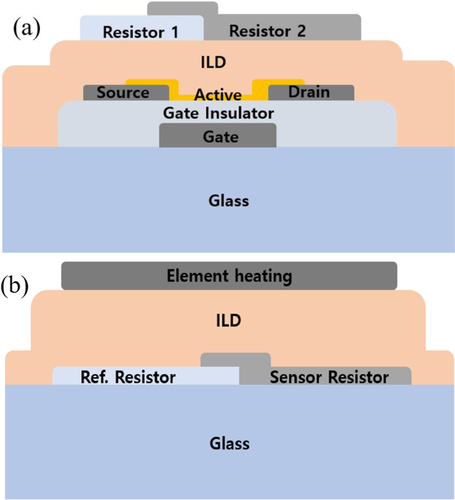
An Al2O3 gate insulator layer measuring 80-nm-thick was deposited via atomic layer deposition (ALD). The gate insulator was patterned by wet etching with phosphoric acid at 80 °C for 3 min for the contact hole to the gate electrode. For the source and drain electrodes, a 150-nm-thick ITO layer was deposited at room temperature by RF magnetron sputtering using an ITO target with an In:Sn atomic ratio of 90:10 and patterned by wet etching. An IGZO active layer with a thickness of 30 nm was deposited via RF magnetron sputtering using a target with an In:Ga:Zn atomic ratio of 2:1:2. The RF power was 50 W and the process temperature was 250 °C. Ar:O2 mixed gas was used with a flow ratio of 22.5:7.5 sccm.
The IGZO layer was patterned by wet etching using a buffered oxide etch (BOE) solution diluted with water at a ratio of 3000:1. The IGZO layer was post-annealed in O2 at 250 °C for 1 h. An interlayer dielectric (ILD) was spin-coated using a negative photoresist (SU-8 2000.5) that measures 1-µm-thick. A 200-nm-thick Ta layer was deposited by DC magnetron sputtering and patterned by RIE with SF6. A 150-nm-thick ITO electrode was deposited by RF magnetron sputtering and patterned by wet etching with photolithography.
2.2. Sample for temperature sensor evaluation
To evaluate the reliability of the temperature sensor, a sample was prepared by attaching a metal heating element to the sensor, as shown in Figure (b). The metal and ITO electrodes were formed on a heater in the same manner as the temperature sensors were on the TFTs. An ILD was spin-coated with 1-µm-thick SU-8 2000.5 insulation to isolate the metal heater electrically from the temperature sensor. A 300-µm-thick aluminium layer was deposited on the ILD layer by DC magnetron sputtering as the element heating layer.
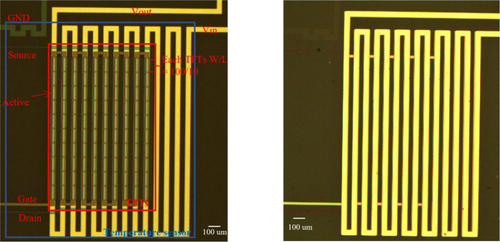
A total of 100 IGZO TFTs were connected in parallel to achieve an effective width of 10 mm and length of 10 µm. Figure shows an optical microscopic image of the temperature sensor on a bottom-gate IGZO TFT. Figure (a) shows each TFT and wiring before the temperature sensor was manufactured, while Figure (b) shows the temperature sensor manufactured on the TFTs. The I–V transfer characteristics of the fabricated TFTs were measured in a dark box. The heat generated by the IGZO TFT during current flow was measured using an integrated thin-film temperature sensor. The thin-film temperature sensor had three electrodes: Vin, ground, and output at the contact point between the two materials.
Figure 2. Optical microscopic images: (a) temperature sensor under IGZO TFT, (b) temperature sensor on IGZO TFT.
The conventional panel-integrated sensor is easily affected by external environmental factors such as external temperature and humidity. These factors can also influence the important electrical properties (e.g. reliability and accuracy) of both the sensor and panel. To minimize external influences on the sensor, a novel temperature sensor that does not require an external resistor was proposed. Two different materials with different temperature coefficients were required to implement the proposed temperature sensor without an external resistor. As mentioned above, the proposed temperature sensor was fabricated and placed on the BGBC-structured IGZO TFTs.
The measurement system was configured as a dark box to avoid exposure to unwanted light. All measurements were performed at room temperature. A DC voltage of 1 V was applied to the temperature sensor to measure the output voltage depending on the temperature. The gate and drain voltages were controlled for heat generation in the TFT. Temperature changes were measured using an embedded thin-film temperature sensor and a forward-looking infrared (FLIR) camera. The distance between the FLIR camera and the heating element or a-IGZO TFTs was approximately 10 cm.
3. Results and discussion
3.1. Temperature sensor evaluation
Several key electrical parameters were extracted to evaluate the electrical performance of the fabricated temperature sensor and TFT. The main electrical parameters were sensitivity, hysteresis for reliability, and repeatability. To evaluate the performance of the temperature sensor, an isolated temperature sensor was fabricated using an aluminium heating element. The output voltage was measured while the source voltage was applied to the aluminium heating element to increase the sensor’s temperature.
The resistance R of the metal changes according to the temperature T and is given by Equations (1–3).
(1)
(1)
(2)
(2)
(3)
(3) where ρ is the resistivity of the temperature-detecting metal electrode, ρ0 is the resistivity at standard temperature T0, and α is the temperature coefficient of the metal electrode. L is the length of the electrode, W is the width of the electrode, and D is the thickness of the metal electrode.
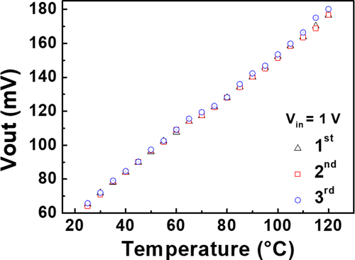
The output voltage of the temperature sensor was measured and analyzed to evaluate the sensitivity, hysteresis, and repeatability of the fabricated sensor. The temperature was measured by activating the heater on the temperature sensor. When the temperature sensor was heated, the output voltage (Vout) was measured with an applied voltage (VDD) equal to 1 V, as shown in Figure . The test range was selected to be 25–120 °C at intervals of 5 °C. The linear fitting curve is shown as a red line. The experimental results were slightly different from the theoretical linear fit curve. The hysteresis of a sensor depends on the state of the sensor and its history. Hysteresis is defined by Equation (Equation4(4)
(4) ).
(4)
(4) where FSO is the full-scale output and the calculated hysteresis is 3.56% FSO. In standard features, a stable sensor has been described with a hysteresis value of 4.49% FSO [Citation21]. Less hysteresis than other typical temperature sensors means that they are much more stable against the measurement history. Sensitivity is also an important electrical parameter in evaluating the performance of temperature sensors. The sensitivity of a sensor can be defined as the minimum input of a physical parameter (i.e. temperature) that creates a detectable output change (i.e. output voltage). In general, the sensitivity of a sensor is defined as the slope of its output characteristic curve. Therefore, the sensitivity of the proposed temperature sensor can be defined by Equation (Equation5
(5)
(5) ), and the extracted sensitivity is 0.85 mV/°C.
(5)
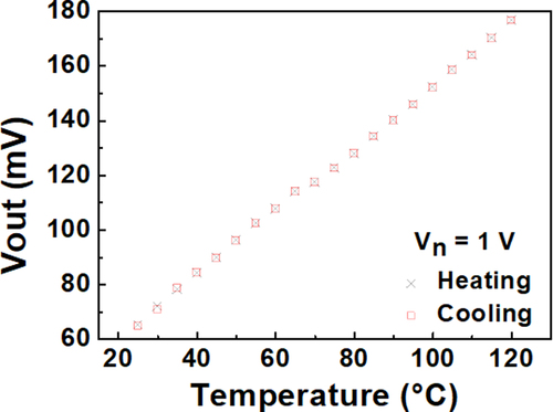
(5) As shown in Figure , hysteresis analysis of the temperature sensor was performed. To evaluate hysteresis, the temperature sensor was measured in two different ways. First, the output voltage of the sensor was measured while increasing the temperature by using an aluminium heating element. The output voltage was then remeasured while decreasing the temperature of the temperature sensor. Ideally, the difference between the heat-up and cool-down measurements should be zero. Notably, almost no hysteresis was observed and no degradation was observed in Vout.
Figure 3. Output voltages and linear fit curve of the proposed temperature sensor.
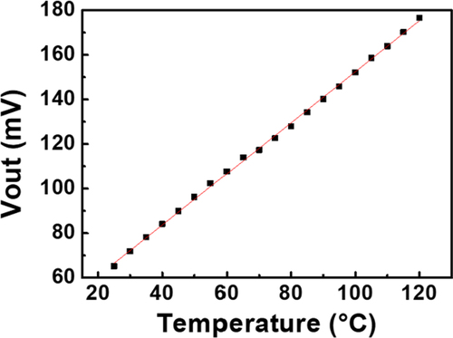
Figure 4. Hysteresis of the proposed temperature sensor.
The last key parameter for evaluating the proposed temperature sensor was repeatability. Repeatability is measured in a short time interval to verify the agreement between values measured by the same people, in the same place, in the same environment, and under the same condition. To test repeatability, the same sensor was measured three times, as shown in Figure . The measured repeatability of the proposed temperature sensor is 0.04 % FSO.
Figure 5. Repeatability of the proposed temperature sensor.
The extracted electrical parameters of the proposed temperature sensor are summarized in Table and compared with those used in other studies. The rated sensor did not exhibit the best performance. However, the proposed sensor exhibited sufficient electrical performance to validate this research. The higher sensitivity reported in Ref. [Citation21] is attributed to the bridge type, which provides a sensitivity two times higher than that of the proposed type.
Table 1. Characteristics of the thin-film temperature sensor.
3.2. Characterization of a-IGZO TFT integrated with a temperature sensor
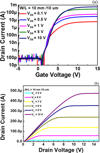
The characteristics of the fabricated a-IGZO TFT with an integrated temperature sensor were measured, as shown in Figure (a) and (b). The device exhibited a field-effect mobility (µFE) of 8.2 cm2V−1·s−1, threshold voltage (VTH) of 5.2 V, ION/IOFF ratio of 8.4 × 10⁶, and subthreshold slope (SS) of 0.52 V·dec−1. The extracted mobility value was obtained from the drain current equation in the saturation regime. TFTs have been manufactured and demonstrated to exhibit correct behaviors, even when embedded in temperature sensors. Results showed that the a-IGZO TFTs were ready for use in a display backplane with sufficient electrical properties.
Figure 6. Electrical characteristics of the amorphous IGZO (a-IGZO) TFTs with a thin-film temperature sensor on it. (a) Transfer characteristics and (b) output characteristics.
Many studies have reported that the characteristics of oxide TFTs are easily influenced by illumination. The most commonly used solution for reducing it is to add an LS layer using a metal or black matrix to block incident light. In this study, the temperature sensor acted as the LS layer, so an additional LS process was unnecessary.
To verify the LS effect of the temperature sensor, positive-bias illumination stress (PBIS) measurements were performed with and without the integrated temperature sensor, as shown in Figure (a) and (b). TFTs were measured at VDS equal to 10 V with a stress time in the range of 0–1200 s at 300 s intervals. The characteristic change was reduced with the temperature sensor, as shown in Figure (b), compared with the TFT without the sensor (Figure (a)). The left shift of the threshold voltages is a drawback of oxide TFTs, and its reduction has been studied previously [Citation24–26]. The temperature sensor reduces the voltage shift by blocking the incident light. The instability of oxide TFTs owing to light illumination stress indicates the importance of the LS layer.
Figure 7. Positive-bias illumination stress of the a-IGZO TFTs. (a) Drain current of the a-IGZO TFT without the light-shielding (LS) layer and (b) drain current of the a-IGZO TFT with the LS layer.
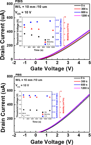
The TFT with the temperature sensor showed a lower threshold voltage than the TFT without the temperature sensor. Because the temperature sensor acts as a back gate, it can affect the threshold voltage of the TFT. Further research on the effect of voltage applied to the sensor electrode is necessary.
The heat generated by the TFT current flow was measured using the fabricated sensor-embedded TFT. Figure (a) shows an optical microscope image of the sensor-embedded TFT, where Vin and Vout are the input and output voltages of the temperature sensor, respectively. The input voltage to the temperature sensor was 1 V, while the output voltage was measured to sense the temperature from the heat generated by the TFT. The drain, gate, and source are the electrodes of the TFT under the temperature sensor.
Figure 8. (a) Optical microscopic image of the TFT with an embedded temperature sensor, forward-looking infrared (FLIR) images at (b) VDS = 5 V, (c) 13 V, (d) 15 V, (e) 18 V (e), and (f) 20 V.
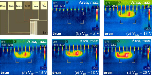
The drain currents of the TFT were increased by increasing the drain bias at a constant gate voltage of 20 V. As the current increases, the temperature of the TFT increases as a consequence of heat generation. The increased temperature was measured using an FLIR camera and a temperature sensor integrated on the TFT.
Figure (b)–(f) show the temperatures measured using the FLIR camera. No noticeable increase in temperature was observed at a low drain voltage of 5 V, as shown in Figure (b). At a drain voltage of 13 V, the temperature increased to 29.8 °C, as shown in Figure (c). The temperatures increased from 29.8–32.9°C when the drain voltage increased from 13 to 20 V, as shown in Figure (c)–(f). The drain current increased to 1.1 mA at a source–drain voltage of 20 V, which resulted in a temperature increase in the transistor to 32.9 °C.
The measured temperatures, output voltages of the temperature sensor, and drain currents are compared in Figure . As the drain current increased from 300 µA to 1.1 mA, the temperature increased from 26 to 32.9 °C, while the output voltage of the temperature sensor increased from 66 to 76 mV. The increased TFT temperature was sensed well by the temperature sensor integrated at the top of the transistor, as summarized in Table .
Figure 9. Measured output voltages of the temperature sensor and FLIR temperature according to the IGZO TFT currents.
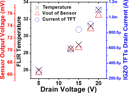
Table 2. Temperature sensor embedded TFT.
This demonstrates the applicability of the integrated temperature sensor for monitoring the temperature distribution on a panel, which enables one to compensate for image distortion by temperature non-uniformity. The display uniformity and performance depend on the temperature distribution. Local heating on the backplane results in an increase in temperature, which consequently increases brightness. A conventional temperature sensor added to the backplane checks a certain point on the backplane. The proposed sensor structure can be used to monitor the temperatures from pixel to pixel by matrix driving on each sensor. Therefore, pixel temperature monitoring is possible as well as TFT threshold voltage and mobility sensing in the external compensation of an OLED. The sensed temperature, threshold voltage, and mobility can be used to adjust the input data signal for uniform display.
4. Conclusion
In general, a temperature sensor that uses the change in the resistance of a metal according to temperature requires an external reference resistance. In this case, a sensing error occurs because the external reference resistance changes with the ambient temperature. A temperature sensor made of serially connected ITO and Ta was used to detect the heat generation of the TFT based on the different temperature coefficients of the two metals. Because the proposed temperature sensor does not require a separate external resistance, it can be integrated into a pixel with reduced sensing error.
Because the materials used are the same as those used in the process of fabricating a display backplane, the proposed temperature sensor can be integrated without additional processes or materials. By integrating it into a pixel, the metal of the temperature sensor can also be used as an LS layer, which can reduce the light-induced instability of oxide TFT.
The integrated temperature sensor on the TFT measured the increased temperature of the TFT with increased drain currents. The measured temperature of the fabricated IGZO TFT under the temperature sensor was 32.9 °C at VDS = 20 V. As the drain current increased from 300 µA to 1.1 mA, the temperature increased from 26 °C to 32.9 °C, and the output voltage of the temperature sensor increased from 66 to 76 mV. The integrated temperature sensors enable us to measure the temperature distribution of a display panel and compensate for image deterioration due to increased temperature.
Acknowledgments
This work was supported by the Technology Innovation Program (P134200017, Development of 1,200 mA class high current-carrying capacity, and 300 K times high-reliability probe unit for super large TV OLED panel inspection), which is funded by the Ministry of Trade, Industry & Energy (MOTIE, Korea).
Disclosure statement
No potential conflict of interest was reported by the author(s).
Additional information
Funding
Notes on contributors

EunSeong Yu
EunSeong Yu received his Bachelor of Engineering from Hoseo University in 2021, and is now pursuing his master’s in the same university. His research is focused on a thermal oxidation TFT, organic TFT, and a temperature sensor.

SeoungGyun Kim
Seoung Gyun Kim received his Bachelor of Engineering degree from Hoseo University in 2022, and is now pursuing his master's in the same university. He has been researching an oxide TFT and a rollable structure.
SeoJin Kang
Seo Jin Kang received her Bachelor of Engineering degree from Hoseo University in 2021, and is now pursuing her master's in the same university. Her research is focused on a gate driver circuit and a pixel circuit as well as optimizing and characterizing circuits.

HyuckSu Lee
Hyuck Su Lee received his Bachelor of Engineering degree from Hoseo University, Asan, South Korea, in 2021. He is now pursuing his master’s degree in the same University. His current research areas include stretchable display driving technology using an a-IGZO TFT.

SeungJae Moon
Seung Jae Moon received his B.S. and M.S. degrees in digital display engineering from Hoseo University, Asan, Chungnam, South Korea, in 2014 and 2017. He received dual Ph.D. degrees in micro-electronics based on inkjet printing technology from Hoseo University, Asan, South Korea, and Rennes 1 University, Rennes, France, in 2020. From 2020 to 2022, he worked as a post-doctoral researcher at CNRS of Rennes 1 University in Rennes, France, particularly on the evaluation of a novel organic semiconducting material for a sensor on a TFT structure and bio-sourced materials for electronics. His current research areas include TFTs, sensors, displays, and integrated circuits of TFTs based on inkjet printing technology.

JongMo Lee
Jong Mo Lee received his bachelor's and master's degrees in digital display from Hoseo University in 2009 and 2011, respectively, and his Ph.D. in semiconductor and display engineering. His research topics comprise a new type of electronic paper, semiconductor processes, TFTs, MEMS, oxide TFTs, and flexible/stretchable displays.

SeungBae An
Seung Bae An received his Ph.D. in machine system design engineering from Tech University of Korea in 2010. From 2010 to 2016, he worked as a research fellow at Korea Instrument, particularly on the development of a NAND and DRAM probe card and MEMS. He has served as Advanced R&D Senior Director at the SP Business Unit of TSE for the development of a NAND and DRAM probe card, System LSI probe card, OLED probe unit, and MEMS since 2016. His current research area involves a hybrid MEMS probe that combines two different probe techniques: a laser bonding type probe and a slit type probe.
ByungSeong Bae
Byung Seong Bae received his B.S. degree in atomic nuclear engineering from Seoul National University, Seoul, South Korea, in 1980, and his M.S. and Ph.D. degrees in applied physics from Korea Advanced Science and Technology, Seoul, South Korea, in 1986 and 1991, respectively. From 1991 to 1998, he worked at Samsung Electronics, particularly on the development of an amorphous and polysilicon TFT backplane with an integrated driver. From 1999 to 2003, he set up a high-temperature polysilicon TFT micro display factory and developed a micro display for projection at ILJIN Display. Since 2006, he has been a professor at the Engineering College of Hoseo University in Asan, South Korea. His current research areas include TFTs, sensors, displays, and integrated circuits of TFTs.
References
- J.S. Park, W.J. Maeng, H.S. Kim, and J.S. Park, Thin Solid Films 520, 1679 (2012).
- D.S. Ji, J.S. Jang, J.H. Park, D.S. Kim, Y.S. Rim, D.K. Hwang, and Y.Y. Noh, J. Inf. Disp 22, 1 (2021).
- M. Kimura, Jpn. J. Appl. Phys 58, 090503 (2019).
- A. Nakashima, Y. Sagawa, and M. Kimura, IEEE Sens. J 11, 995 (2011).
- Y. Chen, S.H. Lee, H.H. Kim, J.S. Lee, D. Geng, and J. Jang, Soc. Info. Disp 28, 528 (2020).
- Y.-S. Shiah, K. Sim, Y. Shi, K. Abe, S. Ueda, M. Sasase, J. Kim, and H. Hosono, Nat. Electron 4, 800 (2021).
- L. Yang, Z.-G. Chen, M.S. Dargusch, and J. Zou, Adv. Energy. Matter 2017, 1701797 (2017).
- Z. Liu, B. Tian, X. Fan, J. Liu, Z. Zhang, Y. Luo, L. Zhao, Q. Lin, F. Han, and Z. Jing, Sens, Actuators A Phys 315, 112341 (2020).
- M. Uenuma, K. Umeda, J. Felizco, D. Senaha, and Y. Uraoka, J. Electron. Mater 48, 1971 (2019).
- K.C. Lee, Y.J. Park, H.W. Park, T. Kim, S.H. Moon, B.H. Berkeley, and S.S. Kim, J. SID 31, 1418 (2006).
- A. Scorzoni, M. Baroncini, and P. Placidi, Sens. Actuators A Phys 116, 137 (2004).
- H.S. Jeon, and B.S. Bae, J. Korean Sensors Soc 19, 483 (2010).
- I. Baía, M. Quintela, L. Mendes, P. Nunes, and R. Martins, Thin Solid Films 337, 171 (1999).
- P. Canhola, N. Martins, L. Raniero, S. Pereira, E. Fortunato, I. Ferreira, and R. Martins, Thin Solid Films 487, 271 (2005).
- C.-W. Kuo, T.-C. Chang, Y.-C. Chien, Y.-L. Tsai, H.-Y. Tu, Y.-C. Tsao, Y.-T. Chien, H.-C. Chen, J.-J. Chen, T.-M. Tsai, and S.M. Sze, IEEE Trans. Electron Devices 68, 1654 (2021).
- T.C. Chen, Y. Kuo, T.C. Chang, M.C. Chen, and H.M. Chen, J. Phys. D Appl. Phys 50, 42LT02 (2017).
- Y.J. Kang, W.B. Lee, J.Y. Kim, K.B. Keum, S.H. Kang, J.W. Jo, S.K. Park, and Y.H. Kim, Mater. Res. Bull 139, 111252 (2021).
- D.P. Gosain, and T. Tanaka, Jpn. J. Appl. Phys 48, 122701 (2012).
- J. Park, H. Kim, P. Choi, B. Jeon, J. Lee, C. Oh, B. Kim, and B. Choi, Electron. Mater. Lett 17, 299 (2021).
- N. Neella, V. Gaddam, K. Rajanna, and M. Nayak, 2016 IEEE 11th Annual Int. Conf. Nano/Micro Engineered and Molecular System 329 (2016).
- H.S. Jeon, S.H. Cho, Y.W. Heo, and B.S. Bae, Mater. Sci. Forum 674, 201 (2011).
- A. Olziersky, P. Barquinha, A. Vilà, C. Magaña, E. Fortunato, J.R. Morante, and R. Martins, Mater. Chem. Phys 131, 512 (2011).
- M. Moreira, E. Carlos, C. Dias, J. Deuermeier, M. Pereira, P. Barquinha, R. Branquinho, R. Martins, and E. Fortunato, Nanomaterials 9, 1273 (2019).
- S.H. Park, E.N. Cho, and I.G. Yun, J. SID 21, 333 (2013).
- T. Matsuda, K. Umeda, Y. Kato, D. Nishimoto, M. Furuta, and M. Kimura, Sci. Rep 7, 44326 (2017).
- D.-B. Jeon, M.-K. Ryu, C.-W. Byun, J.-H. Yang, C.-S. Hwang, and S.-M. Yoon, J. Vac. Sci. Technol. B 33, 020602 (2015).