
ABSTRACT
Flash sintering (FS) is an energy efficient sintering technique involving electrical Joule heating, which allows very rapid densification (<60 s) of particulate materials. Since the first publication on flash-sintered zirconia (3YSZ) in 2010, it has been intensively researched and applied to a wide range of materials. Going back more than a century ago, we have found a close similarity between FS of oxides and Nernst glowers developed in 1897. This review provides a comprehensive overview of FS and is based on a literature survey consisting of 88 papers and seven patents. It correlates processing parameters (i.e. electric field magnitude, current density, waveforms (AC, DC) and frequency, furnace temperature, electrode materials/configuration, externally applied pressure and sintering atmosphere) with microstructures and densification mechanisms. Theorised mechanisms driving the rapid densification are substantiated by modelling work, advanced in situ analysis techniques and by established theories applied to electric current assisted/activated sintering techniques. The possibility of applying FS to a wider range of materials and its implementation in industrial scale processes are discussed.
GRAPHICAL ABSTRACT
Abbreviations: ECAS: Electric Current Assisted/Assisted Sintering; FS: flash sintering; SPS: spark plasma sintering; FSPS: flash spark plasma sintering; HIP: hot isostatic press; HP: hot press; TF: furnace temperature; TOnset: onset temperature; E: electrical field; TS: sample temperature; TSoft: softening temperature for glasses; Tm: melting temperature; PTC or NTC: positive or negative temperature coefficient of electrical resistance; IS: impedance spectroscopy; OES: optical emission spectroscopy; AES: atomic emission spectroscopy; DBS: Dog-bone shape, L: length, W: width, T: thickness, D: diameter, H: height, R: rectangular, CS: cross-section; P: particle size; C: crystallite size; 3YSZ: 3 mol-% yttria-stabilised zirconia; I: ion, H: hole, V: vacancy, E: electron, P: proton
1. Introduction
Sintering is a well-established technique used to consolidate powders by heating green bodies at high temperatures. It involves mass transport, which can occur through solid, liquid or gaseous phases. Sintering, especially on an industrial scale, is usually performed using pressure-less processing in furnaces, and can typically take several hours to complete. To further optimise the properties of sintered materials, several processing techniques have been developed to meet the requirements for materials with novel properties/functionalities. These include pressure-assisted sintering techniques, such as hot pressing (HP) and hot isostatic pressing.
Temperature and pressure are the traditional means to refine the microstructures of densified ceramics. Starting from the 60’s, electric current activated/assisted sintering (ECAS) [Citation1,Citation2] techniques have used to enhance densification. In ECAS, electrical currents or electromagnetic fields might enhance/assist the consolidation process. As reviewed in Grasso et al. [Citation2], the more established ECAS techniques can be divided into two families, Ultrafast ECAS (<0.1 s) and ECAS (>0.1 s), depending on the duration of the electrical discharge. Most of the techniques have discharge times greater than 0.1 s, and this explains why they are commonly referred as ECAS. The threshold of 0.1 s is associated with the use of capacitor dischargers instead of a power supplies, including transformers, inverters and rectifiers. Ultrafast ECAS techniques, typically based on capacitive discharge directly through the sample, are still under development and a few commercial machines are available [Citation3] On the other hand, ECAS includes the well-established spark plasma sintering (SPS) technique (uses Joule heating of conductive dies). Since the 90’s, SPS has been rapidly developed and it is gradually replacing the HP technique. The success of SPS, with nearly 3000 furnaces (number estimated during ‘Electric Field Assisted Sintering Conference’ in Tomar Portugal, March 2016) installed worldwide at present, is attributed to its ability to fabricate nanostructured and metastable bulk materials. In this respect, the rapid heating rate (typically hundreds °C min−1) is undoubtedly a key factor [Citation4]. Also the rapidity of the process has allowed researchers to widen materials compositions and explore different processing parameters. Flash sintering (FS) which involves direct Joule heating of samples (discharge time between 0.1 and 60 s) belongs to ECAS techniques, and sits between Ultrafast ECAS and ECAS.
1.1. FS: terminology before Cologna et al. [Citation5]
In order to better understand the terminology, we clarify how the term FS has been used during the past century. This is to avoid confusion with previous techniques using the same name.
The early stage developments of ECAS techniques were strongly driven by the development of incandescent lamps. In 1905, Johann Lux, an Austrian engineer, communicated his invention to Arthur George Bloxam who was a chemist and also a patent agent (GB patent application number 27,002). In his invention, ‘flash’ (as defined by German [Citation6]) electric current sintering process was used to consolidate tungsten filaments. The fascinating story of the development of tungsten/molybdenum is discussed in detail in a book written by Heerding [Citation7]. We identified several similarities between FS, incandescent lamps and Nernst glowers (Section 1.2, see (a)).
Figure 1. Some snapshots taken from initial work linked to FS. (a) Patent front page of ‘electrical glower light’ dated 1897 taken from original document GB189719424. The lamp described in this document employed a magnesia glower (7 mm length, hollow cylinder outer diameter 1.4 mm and inner diameter 0.4 mm). The glower was first heated using a flame, when it reached a sufficient temperature an AC power source was switched on (0.23 A, 118 V) and the 27 W lamp emitted an intensity of 26 cd (candles). (b) Snapshot of document published in 1908 on electroluminescence of selected oxides [Citation8]. In this work, when the material could not be prepared by melting is was produced by sintering pastes. (c) Drawing showing an experimental setup for FS (see top heading) developed by Hill et al. [Citation9] in 1952. A ceramic lining allowed electrical insulation between the punches and the die, thus allowing current to entirely flow across the powder.
![Figure 1. Some snapshots taken from initial work linked to FS. (a) Patent front page of ‘electrical glower light’ dated 1897 taken from original document GB189719424. The lamp described in this document employed a magnesia glower (7 mm length, hollow cylinder outer diameter 1.4 mm and inner diameter 0.4 mm). The glower was first heated using a flame, when it reached a sufficient temperature an AC power source was switched on (0.23 A, 118 V) and the 27 W lamp emitted an intensity of 26 cd (candles). (b) Snapshot of document published in 1908 on electroluminescence of selected oxides [Citation8]. In this work, when the material could not be prepared by melting is was produced by sintering pastes. (c) Drawing showing an experimental setup for FS (see top heading) developed by Hill et al. [Citation9] in 1952. A ceramic lining allowed electrical insulation between the punches and the die, thus allowing current to entirely flow across the powder.](/cms/asset/db156435-7025-4780-8aac-72a880cf2b3c/yaac_a_1251051_f0001_c.jpg)
Starting from the 40's extensive research on rapid (a few seconds) graphite conversion into diamond using ultra high pressure was carried out at General Electric. The employed technique was described as ‘electric flash-heating’. The term FS was also used by Hill et al. in 1952 in a technical report entitled ‘Production of ceramics by FS process’ [Citation9]. As shown in (c), they referred to FS as a process in which ceramics are sintered in an electrically insulated die (current flows entirely across the powders) by the application of short (order of few tens of ms) single or multiple electrical discharges. In 1966 Storchheim [Citation10] published a US patent, entitled ‘Flash sintering’, on the rapid densification of a biphasic composite achieved by conventional furnace heating above the melting temperature of at least one of the phases (no current flows across the material), resulting in a ‘flash’ (in this case meaning very rapid) sintering process. In 2009, FS was referred to as the instantaneous heating/sintering of metal nano-inks in printed electronics using a Xenon lamp [Citation11].
1.2. FS: terminology after Cologna et al. [Citation5] and analogy with Nernst lamps
More recently, Cologna et al. [Citation5] introduced the term FS while working at Colorado University with Professor Rishi Raj. Their more general and complete definition is given by Raj et al. [Citation12] in a patent application (claim n. 14, the approved patent No US 9,334,194 is slightly different), where FS is described as ‘A method of sintering a material comprising simultaneously exposing the material to an electric field and to heat, such that the material is sintered, wherein the electrical field is between 7.5 V/cm and 1000 V/cm, wherein the onset of sintering is accompanied by a power dissipation between 10 to 1000 mWmm−3, wherein the onset of sintering is accompanied by a non-linear increase in the conductivity of the material, and wherein the time between the onset of sintering and the completion of sintering is less than one minute’. Such definition only suits materials with negative temperature coefficient (NTC) behaviour. In the FS process, when a critical combination of electrical field and temperature (TOnset) is reached, a power surge occurs (the ‘flash event’), resulting in nearly instantaneous full densification in a few seconds [Citation13]. Flash event occurs after an incubation time which depends on field strength electric field and TF.
Nernst developed incandescent lights employing oxide glowers (typically based on magnesia or YSZ) in Göttingen in 1897. Even if the Nernst lamps ((a)) [Citation14,Citation15] were developed more than 100 years earlier than the FS process, there are some strong similarities between them in terms of: (i) material composition; (ii) need of sufficient preheating before applying electric heating; (iii) operation under a current limit in the steady state (materials behave like a glower) to avoid melting of the oxides, which was achieved by having a resistor ballast and a relay in the circuit. In a document published by Coblentz in 1909 [Citation8], a wide range of oxide ceramics were characterised as Nernst Glowers, and electroluminescence was investigated for the following materials: ZrO2 (yttria or calcia stabilised), TiO2, KAlSi3O8, NaAlSi3O8, Be3Al3(SiO3)6, MgO, Porcelain, Glasses, CaF(PO4)3,Ca3(PO4)2, (AlF)2SiO4, Ce2O3, ThO2, U2O3, BeO, Y2O3, Er2O3, Nd2O3, CaO, Co2O3, Cr2O3, SnO2, ZnO, PbO, CaCO3, CaSO4. As discussed below, the materials highlighted by bold font have been processed more recently by FS. This is a surprising finding and it adds some new possible candidates to the list of materials that could be FSed. As stated in the snapshot ((b)) [Citation8], since ceramic pastes were used (instead of dense materials, especially in the case of refractory oxides) the first FS experiments might have been carried out over a century ago. However, it is clear that at that time the main interest was not consolidation, but on the light emission efficiency within the visible range.
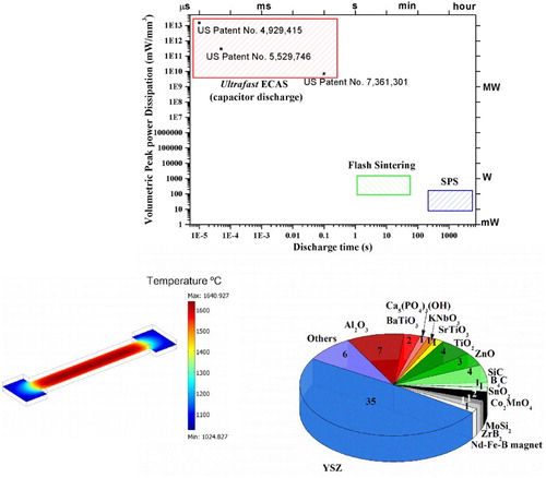
1.3. FS: operating window (peak volumetric power dissipation and discharge time)
A clear differentiation between the various ECAS techniques is highlighted in , where the peak volumetric power dissipation against discharge time is given. It is worth noting that even if the peak volumetric power dissipation does not account for the energy losses (by radiation, conduction (to the electrodes) and convection (surrounding atmosphere)), the data presented is still useful to qualitatively differentiate between the different ECAS processes. By changing the sample geometry (TF and/or other parameters) the power dissipation to produce dense materials is not linearly scalable because of radiative heat losses.
Figure 2. Volumetric peak power dissipation vs. electrical discharge time for different sintering ECAS techniques. The referred operating conditions are taken from typical processing parameters reported in the literature. The peak power density for Ultrafast ECAS was calculated by assuming a sample volume of 63–625 mm3 (current density of 100–1500 A mm−2 and voltages of 3 V–30 kV). The peak power densities in FS are derived from Raj et al. [Citation12], even higher peak dissipation can be reached during switching from voltage to current control mode. The discharge time does not account for incubation time. The peak power densities in SPS have been calculated assuming a power of 1–10 kW for a graphite moulding having diameter of 20 mm.
![Figure 2. Volumetric peak power dissipation vs. electrical discharge time for different sintering ECAS techniques. The referred operating conditions are taken from typical processing parameters reported in the literature. The peak power density for Ultrafast ECAS was calculated by assuming a sample volume of 63–625 mm3 (current density of 100–1500 A mm−2 and voltages of 3 V–30 kV). The peak power densities in FS are derived from Raj et al. [Citation12], even higher peak dissipation can be reached during switching from voltage to current control mode. The discharge time does not account for incubation time. The peak power densities in SPS have been calculated assuming a power of 1–10 kW for a graphite moulding having diameter of 20 mm.](/cms/asset/457dc04f-85cb-45ff-aa8a-f3c3023b9cda/yaac_a_1251051_f0002_c.jpg)
Ultrafast ECAS [Citation16], based on capacitive discharge, is mainly used to sinter electrically conductive metals and cermets (ceramic–metal composites). It employs a capacitive discharge lasting less than 0.1 s, uniaxial pressures up to 1 GPa and a very high peak power dissipation (>109 mW mm−3) [Citation2]. Because of the very rapid discharge most of the heat is directed to the sample and the energy losses during the discharge are minimal. This allows an estimation of the volumetric energy needed for the consolidation in J mm−3. Power densities/discharge times exceeding the ones used in Ultrafast ECAS results in wire explosion techniques used for the fabrication of spheroidal nanoparticles [Citation17]. Apart from the different electrical discharge times, Ultrafast ECAS [Citation2] and FS show two distinctly different processing features: (i) unlike Ultrafast ECAS, FS might require preheating of the material above TOnset; (ii) while Ultrafast ECAS is mostly suitable for electrically conductive (conductivity 105–109 S cm−1, sample geometry should also be accounted for) materials, FS has been also used to densify materials with much lower electrical conductivity such as semiconductors and ionic conductors. In Ultrafast ECAS, to achieve dense and homogeneously sintered materials the sample diameter is kept below 10–15 mm, this limitation does not apply to FS.
As shown in , FS discharge times lie between that of Ultrafast ECAS and SPS and typically fall between an interval of 1–60 s. A comparison with other consolidation techniques having dwelling time well above 60 s is given in Vaidhyanathan [Citation18]. The FS peak volumetric power dissipation ranges between 100 and 3000 mW mm−3, which is much larger than for SPS (10–100 mW mm−3). The absence of an electrically conductive mould (graphite) in FS reduces the thermal inertia from a few hundred grams (mould, punches and sample required for SPS) to a few grams (mostly sample weight). The FSed materials experience a very rapid self-heating approaching tens of thousands °C min−1 combined with a short or no dwell time. This explains why the sintering rate in the FS regime is several orders of magnitude greater compared to SPS [Citation19]. Self-propagating high-temperature synthesis is another rapid processing technique. It differs from ECAS in that the heating is provided by the chemical reactions rather than Joule heating.
1.4. FS: family of materials with different conductivity modes (electronic and ionic)
Electrical conductivity is a key parameter in the FS process, and it can be used to differentiate between materials. Following the first report on 3YSZ, FS has been applied to a wide range of metallic conductors, ionic conductors, semiconductors (with a range of band gaps) and room temperature insulators (wide band gap semiconductors). Electronic conductors (conduction based on holes or electrons), depending on their level of conductivity, can be grouped as insulator, semiconductor or metallic conductors, the ranges are marked in (right side). The flow of charge species in solids driven by an electric potential difference can be complex and different conductivity modes (electrons, holes, ions and defect dipoles in AC mode) might be concurrent. To give an example, α-alumina [Citation20] (purity >99.99%) behaves as a mixed conductor, being predominantly an ionic conductor at temperatures below 873°C, an electronic conductor at temperatures higher than 1323°C and a mixed conductor within the two temperatures ranges.
Figure 3. The temperature-dependence of conductivity of typical metallic, semiconductor (narrow and wide band gap) and ionic conductor, W (Tm = 3380°C) [Citation21], Cu (Tm = 1084°C) [Citation22], B4.3C (Tm* = 2447°C) [Citation23], SiC (Tm* = 2730°C, 3.1 eV) [Citation24], YSZ (Tm ≈ 2700°C) [Citation25], BaTiO3 (Tm = 1618°C, 1.55 eV) [Citation26], Al2O3 (Tm = 2050°C) [Citation27]. Colour coded: metals (grey), semiconductors (green), oxygen ion conductors (blue) and insulating oxides (red). * The material might decompose before melting.
![Figure 3. The temperature-dependence of conductivity of typical metallic, semiconductor (narrow and wide band gap) and ionic conductor, W (Tm = 3380°C) [Citation21], Cu (Tm = 1084°C) [Citation22], B4.3C (Tm* = 2447°C) [Citation23], SiC (Tm* = 2730°C, 3.1 eV) [Citation24], YSZ (Tm ≈ 2700°C) [Citation25], BaTiO3 (Tm = 1618°C, 1.55 eV) [Citation26], Al2O3 (Tm = 2050°C) [Citation27]. Colour coded: metals (grey), semiconductors (green), oxygen ion conductors (blue) and insulating oxides (red). * The material might decompose before melting.](/cms/asset/55c24605-6e08-4d9b-ad28-e5af1a41b1d3/yaac_a_1251051_f0003_c.jpg)
Conductivity is influenced by intrinsic material properties such as the electronic structure, nature of bonding [Citation28], presence of defects [Citation29], grain size, stoichiometry, relative density, crystallinity and level of impurities. It also can be controlled by other environmental conditions such as atmosphere, temperature, pressure, magnetic fields, electromagnetic irradiation, etc.
Even if conductivity has been well studied for more than a century, the data reported typically refers to measurements done under small probing voltages. At present it is not fully understood how field strength (combined with sample heating) affects the conductivity of materials during the FS process. In applied voltages of up to tens of kV (not exceeding electrical breakdown), oxide insulators (Al2O3, and SiO2, MgO, TiO2, and SrTiO3) show a non-linear Ohmic increase in conductivity as a function of electric field [Citation30]. These mechanisms have so far only been investigated at room temperature, and because of this they may not be strictly applicable to FS. Higher temperatures, typically around TOnset, are sufficient to promote complex ionic conditions and other effects such as electrochemical reduction (discussed in Section 4.1.6).
To give some idea of the complexity involved, the room temperature electrical conductivity of oxides spans over an impressive 22 orders of magnitude encompassing insulating, semiconducting, and metallic behaviour [Citation31]. A simplified schematic showing the typical temperature-dependence of electrical conductivity (normalised to their melting/decomposition temperatures) of electronic conductors (metals, insulators, semiconductors) and ionic conductors is given in (for dense materials). The temperature-dependence of conductivity is probably a key parameter in the FS process. It can show a positive temperature coefficient or negative temperature coefficient (PTC or NTC) of electrical resistivity. Most of the ceramics (excluding those that show metallic character) show a NTC of electrical resistivity. With increasing temperature, the electric conductivity of ionic conductors (YSZ) and insulators (BaTiO3, a wide-band gap insulator) increases rapidly, while the conductivity of semiconductors (SiC and B4C) increases at a lower rate. Some materials, for example SiC, experience a transition between intrinsic and extrinsic behaviour at high temperature above an onset temperature. Whereas the conductivity of metallic materials (W and Cu) decreases slightly with increasing temperature (see ) showing a PTC dependence of electrical resistivity.
1.5. Outline of the review
The review is divided into four sections covering processing, materials, mechanisms and modelling. Section 2 defines the FS processing variables. Section 3 on Materials consolidated by FS, is a survey of the materials processed by FS; here particular emphasis is given to densification behaviour, I/V parameters, microstructure and density. In Section 4 Mechanisms of FS, the sintering mechanisms are elucidated from: (i) an empirical analysis linked to the effect of individual processing parameters and (ii) a more general theoretical analysis of the rapid FS densification process. Section 5 on Modelling of FS looks at computational analysis of FS in terms of Joule heating and differential heating within the sample.
2. FS processing variables
2.1. Experimental details for FS
The order of this section follows the typical processing steps performed in a FS run starting from raw powder to a dense bulk.
2.1.1. Green sample preparation and sample geometry
The preparation of green bodies for FS is achieved using well-established ceramic preparation techniques. In the FS process, ceramic powders are uniformly mixed with additives (binder, dispersant or sintering aid) and then shaped into a specific geometry by cold pressing or slip casting. Common geometries include Dog-bone shaped (DBS), cylinder and bar ((a), (b) and (d)). Some of the Flash SPS (FSPS) configurations (uses an SPS machine for carrying out the FS experiments) shown in (c), employ a sample that needs to be strong enough to support the contact force (order of 3–5 kN for a lab-scale SPS machine). The initial sample can be either obtained using cold pressing, carbonaceous binders or pre-sintering. In some other FSPS configurations raw powders [Citation32] are used. Green samples with homogeneous density are desirable, uneven green density might affect the local electrical conductivity and in turn densification. Some effects of sample geometry are given in Section 4.1.7.
Figure 4. Schematic representation of different FS experimental setups: (a) sample is suspended in a furnace using two Pt wire electrodes (adapted from Cologna et al. [Citation33]); (b) sample is pressed between two electrodes (adapted from Caliman et al. [Citation34]); (c) a commercially available SPS machine is used (adapted from Grasso et al. [Citation35]); (d) contactless mode where a plasma is used to carry current across the sample (adapted from Saunders et al. [Citation36]); and (e) setup developed at Rutgers University (RU Tech ID#: 2014-056).
![Figure 4. Schematic representation of different FS experimental setups: (a) sample is suspended in a furnace using two Pt wire electrodes (adapted from Cologna et al. [Citation33]); (b) sample is pressed between two electrodes (adapted from Caliman et al. [Citation34]); (c) a commercially available SPS machine is used (adapted from Grasso et al. [Citation35]); (d) contactless mode where a plasma is used to carry current across the sample (adapted from Saunders et al. [Citation36]); and (e) setup developed at Rutgers University (RU Tech ID#: 2014-056).](/cms/asset/f50d720f-e17a-4895-91bf-0d3a4775ba1c/yaac_a_1251051_f0004_c.jpg)
2.1.2. Sample heating up to TOnset
The sample is heated in a furnace above the critical onset temperature (TOnset) and then sintered in several seconds under an applied electric field above a critical value (ECrit). Several types of furnaces have been used including vertical tubular [Citation37,Citation38], quadrupole lamp [Citation39,Citation40], vertical tubular split [Citation41], a modified box furnace with molybdenum silicide (MoSi2) heating elements [Citation42] and induction heating [Citation43]. Other possible alternatives based on flame heating [Citation44] and arc torch [Citation36] have been also been proposed. It is important to achieve a homogenous sample heating at TOnset, a temperature difference within the sample might result in preferential current flow contributing to inhomogeneous densification.
As shown in (c), in the case of FSPS (employing a single power source), sample heating to TOnset is achieved by integrating a resistive heating source with the sample. This is done by connecting the heating source in parallel with the sample. Once the electrical resistance of the heating source exceeds that of the sample (NTC type) the flash event starts. As reported by Zapata-Solvas et al. [Citation45], one possible heating source is graphite foil interposed between the punches and the electrically insulated mould. Another approach is to use a very thin graphite mould [Citation32], graphite felt [Citation35] or graphite paper [Citation46] as a heating source.
2.1.3. Experimental configurations for FS
The typical FS configurations are shown in . The configurations presented in (a), (d) and (e) are pressure-less while those in (b) and (c) are pressure-assisted. Depending on the furnace and the electrode material, the configuration can be operated in air or in a protective atmosphere such as an inert gas or vacuum.
Out of a total of 88 papers published on FS, 53 of them involve pressure-less mode [Citation33,Citation38,Citation47–49], while 23 involve pressure-assisted ((b) and (c)) [Citation35,Citation42,Citation50]. In the pressure-less configurations, silver (Ag) or platinum (Pt) pastes were employed in order to achieve good electrical contact (minimising contact resistance) between the sample and the electrodes. It is worth noting that these pastes might be co-sintered with the material at the interfaces and it might be difficult to remove and reuse them. Typical electrode materials used for the configuration shown in (a) are Pt [Citation47,Citation51], Ag [Citation52], carbon [Citation53] or stainless steel [Citation54].
Pressure-assisted sintering techniques have the merit of improving the electrical contact at the interfaces between the sample and the electrodes. Cylindrical graphite punches have been used as electrodes [Citation35,Citation43]. For materials susceptible to carbon contamination, refractory metal foils (Ta, Mo and W) can be inserted between the sample and the graphite punches.
Continuous throughput FS techniques are currently under development. As shown in (f), arc plasma has been used to pass electrical current through the sample in a contactless mode [Citation36]. Continuous throughput, involving sliding electrodes has been proposed by Rutgers University, as shown in (e). According to a document circulated by their office of technology and commercialisation, the samples can slide with respect to the electrodes. However, limited data has been published in the open literature on their work. Rolling type FS systems are currently under development at Lucideon (UK) operating in a continuous kiln as briefly mentioned in the conclusion (Section 6). The initial idea of using rolling electrodes started much earlier with the work from Raitchenko (in Russia) as reviewed in the work of Badica et al. [Citation55].
2.1.4. Power supply (DC and AC) and frequency effects
Most FS research has employed DC power supplies (V and I in the range of 10–5000 V and 0.5–15 A, respectively) [Citation5,Citation38,Citation56]. This might be due to their lower cost compared to AC supplies. A few researchers have used AC power supplies (V and I in the range of 10–62 V and 0.1–3 A) operating in the low to mid-range of 50–1000 Hz [Citation54,Citation57,Citation58] and high frequency range of 1 MHz [Citation59]. In the DC mode, the sample mostly behaves as a resistive load, whereas in AC the sample might also show some capacitive/inductive effects. To understand the possible implication of tuning AC frequency during FS, we looked at the report presented by Gittings et al. [Citation60] for hydroxyapatite-based bio-ceramics. They investigated the temperature and frequency dependence of the complex conductivity in the temperature range of 200–1000°C, from DC to 1 MHz (AC). They showed a strong increase (by five orders of magnitude) in the real part of the room temperature conductivity when the AC frequency was increased up to 1 MHz. The trend, which seems applicable to a wider range of dielectrics, might encourage researchers to explore frequency effects in the future.
Up to this point, little attention has been paid to understand how the electrical characteristics of the power supply (e.g. impedance matching of sample, cabling and power supply voltage/current rise time, power spikes, matching between set values and measured ones) can affect the FS sintering process.
2.1.5. Control of the FS process and feedback signal loop
Typically, a conventional sintering process is controlled by its heating profile. In FS, because of its high heating rates, temperature control is difficult to achieve. In most of the FS experiments so far reported, the control was achieved using voltage and current limits. These are simple control modes, which are available in most power supplies. As shown in , the transition from voltage to current control mode creates a power spike [Citation13] which is not to be confused with NTC behaviour of the material. It has been clearly demonstrated that the sample temperature follows the powder dissipation [Citation61]. Even if this control mode ((a)) results in a near instantaneous (5 s) consolidation of the materials [Citation5], it might not be ideal to study or understand the mechanism involved in this process due to its extremely high rate.
Figure 5. (a) Power density and shrinkage relationship in 3YSZ under a field of 100 V cm−1 (DC). (b) Powder density and specimen temperature measured by lattice thermal expansion in situ by synchrotron during FS of 3YSZ under a field of 170 V cm−1 (DC). Adapted from Raj [Citation19] and Lebrun et al. [Citation62].
![Figure 5. (a) Power density and shrinkage relationship in 3YSZ under a field of 100 V cm−1 (DC). (b) Powder density and specimen temperature measured by lattice thermal expansion in situ by synchrotron during FS of 3YSZ under a field of 170 V cm−1 (DC). Adapted from Raj [Citation19] and Lebrun et al. [Citation62].](/cms/asset/e53af13e-ed0b-4533-8cd8-b60e4ce46001/yaac_a_1251051_f0005_c.jpg)
Fully programmable (AC, DC or arbitrary waveform) computer controls which allow real-time adjustment and simultaneous current, voltage and power limits to be applied to any arbitrary time segment are commercially available. These might be a better option for gaining a greater understanding of the FS mechanism. In the case of FSPS, the control mode follows power controls under voltage limits [Citation61].
Once the material has been densified up to a desired level, the FS electrical power can be adjusted/cut off depending on the reading of the electrical resistance, shrinkage and/or a combination of any other output parameters listed in . In order to avoid cracking by thermal shock during cooling, the thermal gradients within the samples should be minimised, and for large components thermal insulation becomes essential [Citation61].
Table 1. Sets of real-time input and output parameters that can be adjusted and recorded during FS.
2.2. FS operating parameters
As listed in , the input parameters can be set to specific values, while output data can be recorded and directly monitored in real time during the FS process. Understanding the relationship between input and output parameters is vital for controlling the FS densification process.
2.2.1. Sample shrinkage during FS
During FS, the sample shrinkage can be measured either using optical methods, such as a CCD camera (shown in (a)) and lasers, or dilatometer techniques based on a linear variable differential transformer (LVDT) (shown in (b)). The true linear shrinkage strain (ϵ) is defined as: ϵ = ln(l/l0), where l0 is the initial length and l is the time-dependent gauge length. As shown in (b), an IS analyser (HP4294A) operating within the range of 40 Hz–110 MHz and 100–200 mV is directly connected with the sample, allowing IS data to be collected during FS. By using this setup is possible to understand the relationship between displacement and impedance data [Citation50].
Figure 6. (a) FS setup and dimensions of DBS green sample (adapted from Naik et al. [Citation63]). (b) Sketch of the experimental setup for dilatometric measurements which can be coupled with impedance spectroscopy during the FS event. LVDT and Pt–Pt 10%Rh thermocouple are used to measure the linear shrinkage. Adapted from Francis et al. [Citation49].
![Figure 6. (a) FS setup and dimensions of DBS green sample (adapted from Naik et al. [Citation63]). (b) Sketch of the experimental setup for dilatometric measurements which can be coupled with impedance spectroscopy during the FS event. LVDT and Pt–Pt 10%Rh thermocouple are used to measure the linear shrinkage. Adapted from Francis et al. [Citation49].](/cms/asset/417a2950-c701-4cf6-897b-2948744537d4/yaac_a_1251051_f0006_c.jpg)
2.2.2. Measurement of sample temperature during FS
Temperature measurements techniques are reviewed by Thomas [Citation64], and in the case of FS dedicated techniques have been developed. The average temperature of bulk specimens controls their densification rates. It is therefore of fundamental importance to obtain accurate measurements in order to understand the kinetics of the FS process. It is challenging to detect the actual specimen temperature directly during FS because of the very rapid thermal runaway, especially for materials having a high NTC. Estimated heating rates in FS range from 103 to 105°C min−1 [Citation35]; these rates are slightly lower than compared to 105–106°C min−1 for incandescent tungsten lamps (inrush current 15 cycles AC 50 Hz, temperature ≈2500°C). The temperature is also expected to show some gradients within the sample on different length scales:
Macroscopic level gradients generated within samples (i.e. TCore–TSurface). The temperature gradient between the core (hotter) and surface of samples exists even within small samples (few cubic millimetres) due to high radiative heat losses.
Microscopic level differential heating induced by phases having different electrical conductivity.
Atomic level due to preferential (electron) scattering occurring at sites having higher crystallographic disorder (dislocations, grain boundaries etc.) [Citation65] or variable chemical composition profiles.
Five methods have been developed to measure TS, including thermocouple, pyrometer (fitting black body radiation), optical emission spectroscopy (OES), impedance analysis, and in situ X-ray diffraction (XRD). The principle and probing location in samples for each method are listed in .
Table 2. Physical principle and probing position for the different temperature measurement methods used in the literature.
2.2.2.1. Thermocouples
Considering the small sample size, thermocouple wires with diameter (D) 0.5–1.5 mm might not be suitable to measure temperature because: (i) slow response time; and (ii) for small samples they might behave as a heat sink unbalancing the sample temperature. The accuracy of a thermocouple readings also relies on the need to maintain electrical insulation (the applied field across the sample might affect the weak signal generated by the thermocouple) with respect to the power supply while requiring good thermal contact with the sample. The electrical insulation and shielding of thermocouple wires is achieved by using thermally insulating oxides, contributing to a delayed response time. In some cases unshielded thermocouples have been used, however unreliable results are expected. As a result, thermocouples might be inadequate to measure the temperature during the transitory heating stage (see power spike in ) of the FS process. When electrical power dissipation reaches a steady state suitable thermocouples might give more reliable readings.
2.2.2.2. Pyrometers and OES
A pyrometer is generally used to detect the surface temperature of specimens, and the integration time for a pyrometer is typically 100 ms. Ultrafast pyrometers with a response time of a few tens of µs are also available. Both single colour (single wavelength) and dual colour pyrometers (dual wavelength measurements) are commercially available, with the latter being insensitive to the sample surface emissivity. Using black body radiation fitting, it was possible to follow in situ (optical fibre inserted within the powder) the temperature evolution with a 100 ms integration time during discharge across a conductive powder as shown in [Citation54].
Figure 7. Emission spectra collected in situ for W powder matching black body radiation and temperatures (obtained from black body radiation fitting) at different time intervals [Citation68].
![Figure 7. Emission spectra collected in situ for W powder matching black body radiation and temperatures (obtained from black body radiation fitting) at different time intervals [Citation68].](/cms/asset/722eeeee-169a-463c-88d9-3363535e0e5f/yaac_a_1251051_f0007_c.jpg)
2.2.2.3. Impedance spectroscopy
Impedance spectroscopy (IS) as a means of in situ thermometry has been used to detect temperature runaway at high temperatures (≥1500°C) in a few seconds in 8YSZ, by translating impedance data into temperature using the corresponding reference electrical resistance data (real part) [Citation69] by taking data at an appropriately high frequency (e.g. 300 kHz). Recorded data (I, V) can be used to probe the bulk sample temperature. This method is in principle applicable to other ceramics. The quality of the measurement relies on the assumption that there is no change in the sample shape and there is no change in the conduction mechanism.
2.2.2.4. Thermal expansion
Thermal expansion has been used to measure the temperature of FS samples [Citation70]. This method can be applied to dense samples while reheating them in FS mode under a dissipated power profile comparable to an FS cycle. By knowing the coefficient of thermal expansion, it is possible to derive the average temperature distribution. Some errors in the readings might be induced by the thermal expansion of the probes heated by the FSed sample.
The temperature can also be determined indirectly using diffraction techniques. XRD was used to determine the temperature during FS of 3YSZ [Citation70]. Unlike the other four methods described above, which can be applied to measure the temperature in real time, this temperature reading is averaged within a volumetric portion of the sample irradiated by an XRD source. As shown in , a specially designed furnace allowed even heating of a specimen to ±3°C.
Figure 8. The arrangement for in situ XRD experiments at the Pohang Light Source II. Adapted from Terauds et al. [Citation71].
![Figure 8. The arrangement for in situ XRD experiments at the Pohang Light Source II. Adapted from Terauds et al. [Citation71].](/cms/asset/12190c96-1f7d-4fc1-beb8-eed91503b7e0/yaac_a_1251051_f0008_c.jpg)
The relationship between lattice parameters and thermal expansion can be used to calculate the sample temperature. By using this method it is possible to detect any difference in the anisotropic lattice expansion between materials heated in FS mode or using a conventional furnace. The change in lattice parameters measured during heating allows an indirect evaluation of the specimen temperature based on the following equation [Citation39]:where Δα/α0 is the change in the lattice parameter, and dhkl and dhkl,0 (derived from peak positions at θhkl and θhkl,0) are the placings at high temperature and at a reference temperature, respectively.
2.2.3. Electroluminescence effect
During FS most of the electrical energy is converted into Joule heating, while a fraction of it is converted directly into radiation. Electroluminescence involves the athermal (it excludes incandescence also known as black body radiation) generation of light by a material when an electric field is applied to it [Citation72]. The wavelength of the absorption and emission lines in the spectra are dependent on material composition and temperature. The optical output recorded during FS has been used to identify any emission induced by the application of an external electric field. Electroluminescence has been well investigated and its significant results are summarised in a comprehensive handbook written by Mueller [Citation73].
2.2.4. Phase analysis
The set-up used for in situ XRD during FS is shown in [Citation40,Citation71]. It is worth noting that any reversible material structural transformation, which might occur when the field is turned off and the material is cooled down to room temperature, might not be captured without in situ techniques. This technique employs a furnace which allows the incident X-ray beam to enter, and the diffracted X-rays to exit and impinge on an image plate detector. Such techniques have identified the formation of an apparent ‘new’ phase during FS of 3YSZ samples [Citation39] and an apparent ‘reversible’ texturing formation only maintained while the field was applied to TiO2 [Citation40] samples. Even if these techniques are very powerful for in situ investigations, the interpretation of the results in terms of precise quantification (lattice parameters and crystal structure) of ‘new’ phase is difficult [Citation39] mainly because of the narrow 2θ range, which is within 1° and the relatively slow acquisition time of 1.5 s.
3. Materials consolidated using FS
3.1. Conductivity mode
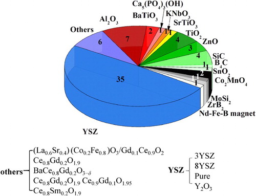
During the past 6 years, FS has been applied to fabricate a wide range of material types: ionic conductors such as cubic and tetragonal yttria-stabilised zirconia (YSZ) [Citation5,Citation39,Citation46,Citation54,Citation66,Citation74,Citation75] and gadolinia-doped ceria (Ce0.8Gd0.2O1.9) [Citation76]; semiconductors and insulators including, alumina (Al2O3) [Citation33,Citation53], barium titanate (BaTiO3) [Citation77], potassium niobate (KNbO3) [Citation78], strontium titanate (SrTiO3) [Citation48], tin dioxide (SnO2) [Citation37], titanium oxide (TiO2) [Citation40,Citation79], zinc oxide (ZnO) [Citation56], silicon carbide (SiC) [Citation43,Citation61,Citation80] and boron carbide (B4C) [Citation32]; as well as several metallic-like non-oxide ceramics (ZrB2 and MoSi2) [Citation35,Citation80,Citation81]. As illustrated in , FSed materials can be grouped with respect to their type of electrical conductivity at TOnset (). Apart from zirconia (and other oxide fuel cell materials), which accounts for most of the publications to date, the other materials in are ordered (clockwise) from low to high electrical conductivity.
Figure 9. Pie chart showing the number of papers published on FS, grouped by material type. The conductivity mechanism (at TOnset) is colour coded: oxygen ion conductors (blue), insulating oxides (red), semiconductors (green), metals (grey). Some materials might show a mixed conductivity mode depending on the temperature. Some of the materials have been consolidated as composites.
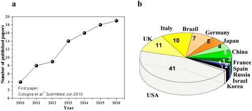
The yearly number of published research papers on FS, up to the end of April 2016, is plotted in (a). During the time needed for publication of the present review (June–September) another 10 papers have been published (and they are not accounted). The expected total number of papers produced in 2016 might approach 40. The countries of origin are given in (b). The number of published papers has increased rapidly during the past 5 years, with a sharp increase over the past 3 years. Nearly 50% (42 out of a total of 88) of the papers have been authored (institution of the first author) by USA scientists ((b)) thanks to the significant contribution by Professor Rishi Raj’s (Colorado University) group. While UK, Italian and Brazilian scientists have also made a significant contribution with 28 publications. Similarly, four out of seven of the patents (approved and applied) related to FS have been registered in the USA.
Figure 10. (a) Research papers published starting from July 2010 till the May 2016. (b) Pie chart showing the nationality of first author’s institution.
3.2. Materials (compositions, electrical data and microstructures)
The published FS literature is summarised in where the FS processing parameters for different material types (ionic, insulator, semiconductor and metallic) are given. The shape of the specimens are mainly dog bone (DBS), the most widely used size has a gauge length 20 mm and cross-section 3 × 1.6 mm2. A comprehensive analysis of the FS behaviour for different materials is given in (a) where the volumetric power dissipation is plotted against the furnace temperature (1000/TF).
Figure 11. (a) Arrhenius plot of volumetric power dissipation for several different ceramics sintered by FS using DC fields. The furnace heating rate was 10°C min−1 and the currents were limited to 80 mA mm−2. The dark grey region with a power dissipation ranging from 7 to 40 mW mm−3 highlights the ‘abrupt’ increase in electrical conductivity of the sample. The sample is DBS with gauge length 20 mm and cross-section 3 × 1.6 mm2. (b) Linear shrinkage measured during FS of 3YSZ under various DC electric fields. (c) Multi-layered NiO–ZrO2 anode to 8YSZ electrolyte with and without the applied field (DC) heated at a rate of 10°C min−1. Adapted from Lebrun et al. [Citation62], Cologna et al. [Citation5], and Francis et al. [Citation49], respectively.
![Figure 11. (a) Arrhenius plot of volumetric power dissipation for several different ceramics sintered by FS using DC fields. The furnace heating rate was 10°C min−1 and the currents were limited to 80 mA mm−2. The dark grey region with a power dissipation ranging from 7 to 40 mW mm−3 highlights the ‘abrupt’ increase in electrical conductivity of the sample. The sample is DBS with gauge length 20 mm and cross-section 3 × 1.6 mm2. (b) Linear shrinkage measured during FS of 3YSZ under various DC electric fields. (c) Multi-layered NiO–ZrO2 anode to 8YSZ electrolyte with and without the applied field (DC) heated at a rate of 10°C min−1. Adapted from Lebrun et al. [Citation62], Cologna et al. [Citation5], and Francis et al. [Citation49], respectively.](/cms/asset/9881e44c-2417-4cc8-adcb-7681fda14564/yaac_a_1251051_f0011_c.jpg)
Table 3. Experimental procedures for FS, including materials, conductivity mode, crystallite size of starting powder, sample size, FS condition current, voltages, relative density and grain size of the produced materials.
3.2.1. FS of ionic conductors
FS was originally developed to sinter ionic conductors such as YSZ. In the first report on FSed YSZ ((b)), a DC electric field was applied to sinter nanograined zirconia (3 mol-% Y2O3–ZrO2, 3YSZ) at ∼850°C, fully densifying the material in a few seconds (<5 s) [Citation5]. Increasing the applied field from 60 to 120 V cm−1, TOnset decreased from 1025 to 850°C ((b)). A long list of publications on 3YSZ and 8YSZ is given in . These publications investigated the effect of processing parameters and configurations. The power density at the onset of the flash is found to be in the range of 7–40 mW/mm–3 ((a)). This suggests that the flash event corresponds to the onset of thermal runaway in materials with highly temperature dependent electrical conductivity as proposed by Todd et al. [Citation13].
Owing to its high ionic conductivity, YSZ (8YSZ) is used as an electrolyte for solid oxide fuel cells (SOFC). DBS samples of 8YSZ have been flash sintered up to 96% theoretical density (TD) using DC currents. Compared to 3YSZ, TOnset decreased to 750°C with an applied DC electric field of 150 V cm−1 [Citation66]. This is a simple consequence of the higher electrical conductivity of the more highly substituted material and the corresponding higher power densities that can be achieved for the same voltage. Downs and Sglavo [Citation38]. further increased the DC field to 2250 V cm−1, resulting in a TOnset as low as 390°C. Self-standing cylinder samples of 8YSZ samples were sintered to 94% TD at a TOnset of 900°C, with an applied AC electric field (1000 Hz, 5 V cm−1, 1 mA mm−2, discharge time: 60 s), using a spring loaded system similar to the setup shown in (b) [Citation75].
A modulated FS technique called hyper flash was developed by Steil et al. [Citation57] In the initial stage, 2000 mW mm−3 of power was applied for several seconds to sinter 8YSZ up to 88% TD with limited grain growth. Subsequent FS at higher power resulted in a more controlled and complete densification [Citation57]. Using a commercial SPS machine, Vasylkiv et al. [Citation46] demonstrated the feasibility of FSPS (20 mm disc shaped samples) using 3YSZ nanoparticles under a voltage as low as 10 V (estimated field ≈2 V cm−1) and a current of 600 A. The sample was preheated using a graphite foil and the effective discharge time for FS was about 10 s.
Yoshida et al. [Citation47] used FS to sinter pure Y2O3 nearly instantaneously to full density at 1133°C (TF) under an applied DC electric field of 500 V cm−1, and its TOnset for FS decreased to 985°C when the electric field was increased to 1000 V cm−1. It is worth noting that Y2O3 is mostly an electronic conductor [Citation47], however, it is presented in this section because it is mostly used to stabilise tetragonal and cubic ZrO2 phases.
FS was applied to multi-layered composites. Green layers of NiO–ZrO2–cubic ZrO2 were flash sintered at TF below 1000°C in a few seconds under the application of a DC electric field (150 V cm−1). FS avoided the typical undesired delamination which occurs during conventional sintering [Citation49]. As shown in (c), the shrinkage behaviour of the multilayer (M) shows an intermediate behaviour between the anode (A) and the electrolyte (E).
shows the microstructures of 3YSZ, 8YSZ and Y2O3 produced by FS. There are 34 published papers which focus on YSZ. Even if rapid grain growth was observed in the FSed 3YSZ and 8YSZ with increasing sintering time, the grain size obtained using FS was smaller than those using conventional sintering. Yoshida et al. [Citation47] densified pure Y2O3 using FS to nearly full density, as shown in (c).
Figure 12. SEM micrographs of (a) 3YSZ, (b) 8YSZ and (c) Y2O3 FSed as described in the text above using DC fields. Adapted from Baraki et al. [Citation86], M'Peko et al. [Citation70], and Yoshida et al. [Citation47], respectively.
![Figure 12. SEM micrographs of (a) 3YSZ, (b) 8YSZ and (c) Y2O3 FSed as described in the text above using DC fields. Adapted from Baraki et al. [Citation86], M'Peko et al. [Citation70], and Yoshida et al. [Citation47], respectively.](/cms/asset/1e31d3d9-2595-46f7-8fb6-3478edf23d62/yaac_a_1251051_f0012_b.gif)
3.2.2. FS of insulators and semiconductors
Semiconductors and insulators have been processed by FS, even if they possess relatively low electrical conductivity at room temperature. They have been grouped together because insulators are wide-band gap semiconductors. As shown in (a), pure alumina (α-Al2O3, band gap: 8.8 eV [Citation99]) remains unaffected even in applied fields up to 1000 V cm−1, due to its very low electrical conductivity (). The latter suggests that the TOnset might be greater than the conventional sintering temperature. However, FS of MgO-doped α-alumina occurred at a TF of 1320°C, and the rapid shrinkage under an applied field of 500 V cm−1, similar to thermal runaway, is shown in (b) [Citation33]. This is because the heating of MgO results in a significant increase of its electrical conductivity. The authors also observed a clear hysteretic current-field response upon application of 800 V cm−1, suggesting a material modification was induced which could be either by ionic migrations by defect redistribution within the material. When the electric field was increased to 1000 V cm−1, TOnset decreased to 1275°C. Compared to conventional sintering (sintered at 1550°C for 1 h, grain size 1.5 µm), FSed MgO-doped Al2O3 using the setup in (a) has a finer grain size of 0.8 µm, as shown in (c) and (d). More recent work by Biesuz and Sglavo [Citation53]. using fields as high as 1500 V cm−1 found a lower TOnset of 900°C for 99.8% pure α-alumina samples. In their work, the bulk density approached 3.9 g cm−3. Two-phase 50 vol.-% 3YSZ–Al2O3 samples with high density (≥95% TD) were obtained using FS at a TF of 1060°C, in an applied electric field (150 V cm−1, current density: 85 mA mm−2) [Citation63].
Figure 13. Effect of applied electric field (0–1000 V cm−1) on the shrinkage for (a) pure Al2O3 and (b) MgO (0.25 wt-% MgO) doped Al2O3. The resulting SEM micrographs for MgO-doped Al2O3 obtained using (c) FS (1000 V cm−1, DC) TF = 1260°C) and (d) conventional sintering (1550°C for 1 h), the resulting grain sizes were 0.8 and 1.5 µm. In both cases the furnace heating rate was 10°C min−1. Adapted from Cologna et al. [Citation33].
![Figure 13. Effect of applied electric field (0–1000 V cm−1) on the shrinkage for (a) pure Al2O3 and (b) MgO (0.25 wt-% MgO) doped Al2O3. The resulting SEM micrographs for MgO-doped Al2O3 obtained using (c) FS (1000 V cm−1, DC) TF = 1260°C) and (d) conventional sintering (1550°C for 1 h), the resulting grain sizes were 0.8 and 1.5 µm. In both cases the furnace heating rate was 10°C min−1. Adapted from Cologna et al. [Citation33].](/cms/asset/e2cbcf22-5c19-426f-9cb9-e55586d364a1/yaac_a_1251051_f0013_b.gif)
There are a few papers reporting the results of FS of BaTiO3 (temperature dependence of conductivity is shown in ), SrTiO3, and KNbO3. Aylin et al. [Citation48] found that both the density and grain size of FSed SrTiO3 decreased with increasing applied voltage, which is opposite to the FS densification behaviour of ionically and other electronically conductive ceramics. This could be attributed to either the significantly lower TF, of about 500°C, when the field was increased from 150 to 1000 V cm−1, thus resulting in lower sample temperature or to other effects. According to a recent work by Naik et al. [Citation100], SrTiO3 flash sinters fully, while its composites with KNbO3 show only limited densification. To our knowledge this behaviour may be attributed to the high tendency of KNbO3 to sublime (compared to SrTiO3) when heated by FS up to high temperature. The resulting sublimation would hinder the densification process especially because of hot spots forming at the particle contact points.
As shown in , DBS SrTiO3 samples (indirect band gap: 3.17 eV [Citation101]) obtained using a FS setup (see (a)) at 150 V cm−1 and 1200°C has a narrower grain size distribution, compared to those obtained using conventional sintering (sintered at 1400°C for 1 h). With applied electric field increasing to 1000 V cm−1 in SrTiO3, TOnset decreased to 640°C. This trend is similar to the one reported for YSZ and MgO-doped Al2O3. In addition, the formation of Ruddlesden–Popper (RP) phases [SrO(SrTiO3)n or Srn+1TinO3 n+1] for FSed samples corresponds to the elimination of a TiO2 layer from the SrTiO3 perovskite structure resulting in a double-layer of SrO. As suggested by Reibold et al. [Citation102], these phases originate either from ordering of oxygen vacancies or electromigration of SrO ion complexes. Future work is needed to correlate RP phase formation to FS processing and its mechanism.
Figure 14. SEM micrographs of SrTiO3 obtained using (a) FS (150 V cm−1 DC), TF = 1200°C) and (b) conventional sintering (1400°C for 1 h). Adapted from Yoshida et al. [Citation47].
![Figure 14. SEM micrographs of SrTiO3 obtained using (a) FS (150 V cm−1 DC), TF = 1200°C) and (b) conventional sintering (1400°C for 1 h). Adapted from Yoshida et al. [Citation47].](/cms/asset/b2e93191-df16-41fc-97d4-360f044c8466/yaac_a_1251051_f0014_b.gif)
BaTiO3 (band gap: 3.42 eV [Citation103]) is a polar, ferroelectric material. Using FS, starting from green samples in the shape of a bar, a 94% TD and fine grain size ((a)) were obtained at a TOnset of 688°C in an electric field of 500 V cm−1 [Citation94]. A secondary phase (BaTi4O9), not seen for conventionally sintered materials, was produced at the grain boundaries, as shown in (b) [Citation77]. This is possibly due to the effect of electric field on the oxygen diffusion or electrochemical reduction. A more detailed analysis about this effect is currently under investigation.
Figure 15. (a) Microstructure of FSed BaTiO3 at an applied voltage (DC) of 250 V cm−1 and current limit of 9.3 mA mm−2, TF = 822°C. (b) TEM bright field image and the electron diffraction pattern of a secondary phase in flash-sintered BaTiO3 at an applied voltage of 100 V cm−1 (DC), TF = 1020°C for 60 s. (c) Microstructure of flash-sintered KNbO3 with applied electric field of 600 V cm−1 (DC), TF = 750°C. Adapted from M'Peko et al. [Citation94], Uehashi et al. [Citation77], and Shomrat et al. [Citation78], respectively.
![Figure 15. (a) Microstructure of FSed BaTiO3 at an applied voltage (DC) of 250 V cm−1 and current limit of 9.3 mA mm−2, TF = 822°C. (b) TEM bright field image and the electron diffraction pattern of a secondary phase in flash-sintered BaTiO3 at an applied voltage of 100 V cm−1 (DC), TF = 1020°C for 60 s. (c) Microstructure of flash-sintered KNbO3 with applied electric field of 600 V cm−1 (DC), TF = 750°C. Adapted from M'Peko et al. [Citation94], Uehashi et al. [Citation77], and Shomrat et al. [Citation78], respectively.](/cms/asset/9fb12181-7e55-4e90-a6b0-009e4be2c3a7/yaac_a_1251051_f0015_b.gif)
Potassium niobate (KNbO3), a lead-free ferroelectric material, has gained much attention because of its properties and environmentally friendly composition. Because of its tendency to sublime, it is difficult to consolidate to full density while maintaining its stoichiometry. Recently, stoichiometric KNbO3 with 95% TD ((c)) was obtained using FS (applied voltage: 600 V cm−1, TF = 750°C) [Citation78]. Even if though its TF of 750°C was close to the 800°C, which results in rapid volatilisation of K2O, dense materials could still be obtained thanks to the very rapid FS processing. The piezoelectric properties of FSed KNbO3 have not been reported.
Zinc oxide (ZnO, band gap: 3.3 eV [Citation104]) is an n-type semiconductor material used in electronic and optoelectronic devices. Schmerbauch et al. [Citation41] consolidated cylindrical ZnO samples with homogenous and non-graded microstructures using the FS setup shown in (b), under an applied AC electric field of 160 V cm−1 and 50 Hz (max current was 3.75 A when the field was 160 V cm−1). The applied electric field significantly improved the density of the material, as shown in (a) and (b). As shown in (c)–(f), the grain size of ZnO increased with increasing electric field (above 80 V cm−1), which is also proportional to the volumetric power dissipation and TS. Compared to a previous study employing an AC power source, Zhang and Luo [Citation96] obtained cylinder ZnO specimens with a relative density of >97% TD and fine grain sizes of ∼1 µm using the FS setup shown in (b) (DC, discharge time ∼30 s, TF < 120°C, atmosphere Ar + 5 mol-% H2). Bi2O3 doping was applied to eliminate the anode-side abnormal grain growth via a liquid-phase sintering effect, resulting in ZnO with a more homogenous microstructures [Citation55].
Figure 16. Microstructures of ZnO obtained using at 80 V cm−1 (AC) stopped (a) before and (b) after FS as well as fully sintered specimens at (c) 0 V cm−1 for 2 h, (d) 40 V cm−1 for 1 h, (e) 80 V cm−1 for 2 h and (f) 160 V cm−1 1 h, with TF = 700°C. Current densities were between 54 and 151 mA mm−2. Adapted from Schmerbauch et al. [Citation41].
![Figure 16. Microstructures of ZnO obtained using at 80 V cm−1 (AC) stopped (a) before and (b) after FS as well as fully sintered specimens at (c) 0 V cm−1 for 2 h, (d) 40 V cm−1 for 1 h, (e) 80 V cm−1 for 2 h and (f) 160 V cm−1 1 h, with TF = 700°C. Current densities were between 54 and 151 mA mm−2. Adapted from Schmerbauch et al. [Citation41].](/cms/asset/8b2256ca-9415-40ea-abf9-733b416d3968/yaac_a_1251051_f0016_b.gif)
Tin oxide (SnO2) is an n-type semiconductor used in chemical sensors, solar cells and battery applications. Green pellets of SnO2 were sintered to high density (94% TD) at a low TOnset of 900°C, which is 400°C lower than its conventional sintering temperature, with the application of an AC electric field (80 V cm−1, 1 kHz, 5 A) [Citation58]. The presence of 2 wt-% MnO2, as a sintering aid, was effective in further increasing the density.
Semiconductor α-SiC (band gap: 3.05 eV [Citation105]) was nearly fully densified using FS (configuration similar to the one given in (b)) in the presence of sintering aids (Al2O3 and Y2O3) under an applied electric field of 100 V cm−1 and TF of 1170°C [Citation80]. Using the setup shown in (c), FSPS was applied to densify discs of β-SiC 10 wt-% B4C (D = 20 mm) and α-SiC powders (D = 60 mm) up to relative densities of 96 and 98% using a discharge time of 17 and 60 s, respectively, under an applied pressure of 16 MPa [Citation61]. By extending the processing times or by using pure SiC powders, FSPS was used to densify SiC while simultaneously inducing texturing. The mechanisms for the formation of textured microstructures were attributed to the directional physical vapour transport [Citation43] driven by the thermal gradient developed within the samples during the FSPS process.
Boron carbide (B4C) is a lightweight and hard ceramic material widely used in amour and as a high-temperature p-type semiconductor. Because of its semiconductor nature and its strong NTC behaviour (), B4C samples could be densified by FSPS using a modified setup employing a thin graphite mould (FSPS setup similar to the one shown in (c)). Niu et al. [Citation32] densified B4C powder up to 99.2% TD in 60 s with limited grain growth at 1931°C (die surface temperature clearly underestimating the Ts), under an applied pressure of 15.3 MPa.
3.2.3. FS of metallic-like conductors
Metallic conductors will behave differently to ionic and semiconductor materials because of their PTC behaviour. This means that they do not thermally runaway in the same way. In order to achieve high heating rates you have to provide an excess power density. However, metallic-like conductors have the advantage that they are electrically conductive from room temperature. It is worth to mention that in some cases pressed powders might show limited conductivity because of their surface oxide layer. When using capacitive discharge methods they can be sintered in a few µs (). Despite their high conductivity, these technique have not been able to consolidate materials which are as strongly refractory, such as the borides nitrides and carbides of transition metals.
Co2MnO4 spinel, an electronic conductor, is generally used to protect metals from oxidation at high temperature in SOFC. Prette et al. [Citation37] FSed it in a few seconds at ∼325°C, under a DC field of 12.5 V cm−1, as shown in (a). Meanwhile, the FSed Co2MnO4 avoided the formation of interconnected pores which existed in conventional sintered Co2MnO4.
Figure 17. (a) SEM micrograph of FSed Co2MnO4 (DC). (Adapted from Prette et al. [Citation37]). (b) The relative density and grain size vs. discharge time for FSPSed (pulsed DC) ZrB2 sample and (c) SEM microstructure of ZrB2 after 35 s discharge. (Adapted from Grasso et al. [Citation35] (d) SEM micrograph of Nd–Fe–B type permanent magnetic material with aligned nanocrystalline platelike grains. Adapted from Castle et al. [Citation98]).
![Figure 17. (a) SEM micrograph of FSed Co2MnO4 (DC). (Adapted from Prette et al. [Citation37]). (b) The relative density and grain size vs. discharge time for FSPSed (pulsed DC) ZrB2 sample and (c) SEM microstructure of ZrB2 after 35 s discharge. (Adapted from Grasso et al. [Citation35] (d) SEM micrograph of Nd–Fe–B type permanent magnetic material with aligned nanocrystalline platelike grains. Adapted from Castle et al. [Citation98]).](/cms/asset/cbeed7b7-d49b-4c48-99df-75ca5da1aa11/yaac_a_1251051_f0017_c.jpg)
Pure ZrB2 monoliths with a density of 95% were obtained using FSPS in 35 s with the application of pressure (16 MPa) and DC electric field [Citation35]. The grain size of ZrB2 increased rapidly when the discharge time in FSPS increased from 25 to 35 s, as shown in (c). A novel system with an electrically insulated graphite die allowed MoSi2 and ZrB2/20 vol.-% MoSi2 to be sintered in less than 60 s with heating rates of over 2000°C min−1 with much lower energy consumption compared to conventional SPS [Citation45].
Nd–Fe–B type permanent magnetic material with aligned, nanocrystalline platelike grains was obtained using a 30 s SPS pre-sintering step. During a 10 s discharge, FSPS [Citation98] resulted in a very rapid deformation induced by the rapid heating under an uniaxial pressure. The resulting microstructure was composed of nano-platelet grains oriented in a direction perpendicular to the applied load ((d)), and the marked anisotropic magnetic properties obtained for FSPSed materials were comparable to hot forged materials.
The overview of the experimental observations described above suggests that FS is essentially a thermal runaway phenomena in ionic and semiconductor materials. With suitable control it is possible to achieve high heating rates and controlled sintering with minimal grain growth. However, the high heating rates and the direct electrical heating can lead to additional interesting effects, such as electromigration, electroluminescence and electroplasticity. The evidence for these effects is reviewed in the next section.
4. Mechanisms of FS
This section is divided into two subsections. The first one (4.1) aims to improve the understanding of the FS mechanism by empirically investigating the role of each processing variables given in . In the second section (4.2), FS densification mechanisms are presented.
4.1. Effects of processing parameters on sintering behaviour
4.1.1. Electric behaviour (field and polarity effects)
As shown in , most of the papers (46) used a DC electric field (five of them are related to pulsed DC using FSPS), while only 11 papers employed AC. An obvious reason for this is the significant price difference between the AC and DC power supplies. Considering the limited number of studies, it is difficult to obtain a comprehensive understanding of DC and AC effects on FS behaviour. However, clearly marked polarity effects are expected in the DC mode, as discussed below in Section 4.1.6.
Under the influence of an electric field, sintering behaviour can be divided into two regimes [Citation5,Citation38]: (i) below ECrit characterised by moderately increased sintering rates; and (ii) above ECrit or in the FS regime, characterised by rapid (a few seconds) sintering to near full density. Referring to (b), by increasing electric field, the transition from one regime to the other occurs gradually in single-phase titania [Citation40], barium titanate [Citation97] and zirconia/alumina [Citation92], but abruptly in 3YSZ. It increases with decreasing electric field, as shown in (b). Power dissipation in the sample is the determining factor for the initiation of FS. Downs and Sglavo [Citation38] investigated the relationship between electric field (E) on the TOnset of FS, discovering and empirical relationship TOnset (K) = 2440 E−1/5.85 (V cm−1), and the effects of power dissipation and current density on densification of cubic ZrO2. At present the charge carriers involved in the Joule heating have not been identified so it is difficult to understand the incubation stage. As discussed in the section below, TOnset and the incubation time might not just depend on the field but also other parameters presented in the sections below, including sintering atmosphere, crystallite size, external mechanical pressure, sample size, etc.
Figure 18. (a) Temperature of 8YSZ samples (0.6–0.9 mm thick) under constant voltage (8–8.5 V (DC)) as function of time (no current limit). Inset: decrease in resistance (AC real component) divided by its room temperature reference value. (b) Empirical relationship between DC electric field and incubation time for FS of 3YSZ at different isotherms TF (1000, 1200, 1275 and 1300°C). Adapted from Park and Chen [Citation69] and Naik [Citation106], respectively.
![Figure 18. (a) Temperature of 8YSZ samples (0.6–0.9 mm thick) under constant voltage (8–8.5 V (DC)) as function of time (no current limit). Inset: decrease in resistance (AC real component) divided by its room temperature reference value. (b) Empirical relationship between DC electric field and incubation time for FS of 3YSZ at different isotherms TF (1000, 1200, 1275 and 1300°C). Adapted from Park and Chen [Citation69] and Naik [Citation106], respectively.](/cms/asset/6ec2a60d-45a6-4535-aae4-9b312abdcb23/yaac_a_1251051_f0018_c.jpg)
4.1.2. Effect of particle size
The effect of particle size (1, 2, 5 and 10 µm) in FS in DC mode on the TOnset, microstructure (grain size distribution) and density of 3YSZ was investigated during heating from 920 to 1040°C at a rate of 10°C min−1 [Citation82]. TOnset increased with increasing particle size ((a)). This was attributed to the higher power absorption (lower resistivity) of finer grained particles. However, the mechanism determining this behaviour has not been yet clarified, and it should not simply be attributed to electrical conductivity which is higher for nano grained materials compared to single crystal as in the case of 10YSZ films [Citation107]. Also finer grained materials have a greater tendency to form necking (resulting in higher conductivity) during heating as seen for the 0 V curve in (a). This might explain the lower TOnset temperature for finer particle size. Future work is needed to clarify the dependence between the grain size and TOnset, similarly the effect of crystallite (both for green powders or dense bulk) size is still to be clarified. Another aspect to consider is the lower conductivity of polycrystalline materials compared to single crystal for 8YSZ. As shown in (b and c), under a field of 150 V cm−1, dense single crystal can be heated in FS mode at a TOnset as low as 400°C, while the polycrystalline materials need at least 600°C. The mechanism of heating seems primarily to be driven by the conductivity rather than any other effect.
Figure 19. (a) Effect of particle size on the FS behaviour of 3YSZ, the shrinkage is plotted against furnace temperature with and without field (100 V cm−1 (DC)) (Adapted from Francis et al. [Citation82]). (b) Difference in conductivity for polycrystalline and single crystal 8YSZ and (c) the resulting power absorption of dense specimens while heating in flash mode. The figures were kindly provided by Professor Jian Luo from University of California, San Diego Jian Luo PDP. 2016. Private communication.
![Figure 19. (a) Effect of particle size on the FS behaviour of 3YSZ, the shrinkage is plotted against furnace temperature with and without field (100 V cm−1 (DC)) (Adapted from Francis et al. [Citation82]). (b) Difference in conductivity for polycrystalline and single crystal 8YSZ and (c) the resulting power absorption of dense specimens while heating in flash mode. The figures were kindly provided by Professor Jian Luo from University of California, San Diego Jian Luo PDP. 2016. Private communication.](/cms/asset/0c8f0018-a681-4ef7-88a6-5d9d314ef33b/yaac_a_1251051_f0019_c.jpg)
4.1.3. Effect of pressure
It has been demonstrated that external pressure can greatly increase the driving force for densification without affecting the driving force for grain growth [Citation4,Citation108]. External pressure plays a significant role in increasing the level of green compaction by particle rearrangement and enhancing the rate of pore closure [Citation42]. It is difficult to compare results with or without pressure because different configurations () have been employed.
In the case of 3YSZ with a starting crystallite size of 50 nm under an applied pressure of 12 MPa, a field of ∼72 V cm−1 results in FS and a TF ranging from 850 to 920°C. TOnset in FS decreased with increasing pressure (shown in ). This might be attributed to the higher level of compaction and enhanced necking resulting in improved conductivity (see Section 4.1.2).
Figure 20. Shrinkage strain of 3YSZ samples under different uniaxial pressures using the setup shown in (b) in a 100 V cm−1 applied field. Adapted from Francis [Citation54].
![Figure 20. Shrinkage strain of 3YSZ samples under different uniaxial pressures using the setup shown in Figure 4(b) in a 100 V cm−1 applied field. Adapted from Francis [Citation54].](/cms/asset/19301d31-9e82-4514-81d0-e2fd2f66ef28/yaac_a_1251051_f0020_c.jpg)
4.1.4. Effect of atmosphere
The atmosphere in contact with the sample during FS can be varied from highly oxidising (ozone or oxygen rich) to highly reducing (hydrogen). In equilibrium conditions the atmosphere can control the vacancy concentration in the material and affect its conductivity. For n-type conductors, such as SnO2 and TiO2, conductivity varies inversely with oxygen partial pressure. For p-type conductors the opposite behaviour has been reported for CeO2 and ZrO2. In general, using a reducing or oxidising atmosphere, one can distinguish between hole or electron conduction modes.
The conductivities (ionic, electronic and holes) in 8YSZ has been well investigated in condition of thermodynamic equilibrium [Citation109]:
where
is the oxygen partial pressure. The change in conductivity is related to a reversible vacancy accumulation when the material is heated in an atmosphere containing variable oxygen partial pressure.
The significance of atmosphere on FS has been seen as a reduction in the TOnset using ZnO as a model material system [Citation96]. Zhang et al. has specifically investigated the effect of atmosphere (air or flowing gas of Ar, Ar + 5 mol-% H2 and O2) on FS [Citation56,Citation99]. A more reducing hydrogen atmosphere (Ar + 5 mol-% H2) led to the reduction in the TOnset down to 186°C, while pure O2 atmosphere increased TOnset = 631°C only slightly compared to air TOnset = 599°C (shown in (a)). The reduction of TOnset may be due to the increased electrical conductivity of polycrystalline ZnO under reducing atmosphere [Citation110], as shown in (b).
Figure 21. (a) Measured electric power dissipation plotted against furnace temperature and (b) measured conductivity as function of the reciprocal of the estimated TS for FS ZnO using four different atmospheres (in a 300 V cm−1 DC electric field). Adapted from Zhang and Luo [Citation96].
![Figure 21. (a) Measured electric power dissipation plotted against furnace temperature and (b) measured conductivity as function of the reciprocal of the estimated TS for FS ZnO using four different atmospheres (in a 300 V cm−1 DC electric field). Adapted from Zhang and Luo [Citation96].](/cms/asset/13272943-e73a-4fb1-a0aa-1cd6c012bff1/yaac_a_1251051_f0021_c.jpg)
4.1.5. Effects of electrode material and its catalytic activity
In ionic conductors, the interaction between the ionic charge carriers and electrode material appears to be a key factor for the occurrence of FS. Apart from generating a potential drop across the sample, the electrodes might influence the rate of flow of ionic charge. Pt has been commonly used as the electrode material for FS oxygen ionic conductors (i.e. YSZ). Pt not only has the merit of being oxidation resistant up to high temperatures in air, but also might play a role in terms of catalytic activity in the exchange of oxygen at the electrodes. More recently FSPS employing graphite electrodes has been used for 3YSZ [Citation46], however, electrode effects were not analysed in the paper.
As shown in , Ag used as electrode material contributed to the occurrence of FS in the case of β-Al2O3. Pt electrodes did not allow current flow since there was no charge exchange between the electrode and electrolyte (Li+ or Na+ were identified as charge carriers) [Citation34]. FS of α-Al2O3 [Citation53] showed a similar behaviour, compared to carbon or Pt, an enhancement of electrical conductivity in the presence of Ag electrodes was found. Efficient electrochemical transfer at the Ag/β-Al2O3 interface has been reported to promote a flash event in MgNa2Al10O17 [Citation34]. In summary electrode materials might play a very significant role during the incubation stage allowing ion movement which could affect the conductivity.
Figure 22. FS attempts in β-Al2O3 with different electrode materials and atmospheres during isothermal at 550°C under an applied AC field of 100 V cm−1 (AC). FS occurred when Ag electrodes were used instead of Pt. Adapted from Caliman et al. [Citation34].
![Figure 22. FS attempts in β-Al2O3 with different electrode materials and atmospheres during isothermal at 550°C under an applied AC field of 100 V cm−1 (AC). FS occurred when Ag electrodes were used instead of Pt. Adapted from Caliman et al. [Citation34].](/cms/asset/39ab547f-671d-4200-ba53-60f0e6b74e78/yaac_a_1251051_f0022_c.jpg)
In the case of metallic conductors there is no significant effect induced by the electrode material. Inexpensive graphite electrodes have been applied to fabricate ZrB2 [Citation35]. In the case FS of semiconductors, such as SiC [Citation61] and B4C [Citation32], there is a metal–semiconductor junction, which produces Schottky barriers.
4.1.6. Polarity induced effects
Most of the published work does not account for polarity induced effects, which are expected when DC fields are applied. When a potential drop is applied across a bulk sample, depending on the conductivity mode, several polarity effects became apparent. At present some of these effects have not been fully investigated. Bulk effects (within the FSed sample), contact effects (interface sample electrode) and electrode effects (effects within their own bulk) in FS play a critical role in the densification of materials. The bulk effects are summarised in .
Table 4. Bulk effects occurring within the material as result of DC bias applied across sample during FS.
Bulk effects in metals have been well investigated and are reported elsewhere [Citation111].
Contact effects between electrode and sample might also play a role but they have not been extensively investigated. Assuming that the electrode is a metallic conductor, depending on the mode of conductivity of the FSed materials, different effects can be expected: (i) contact resistance for metallic conductors, (ii) metal–semiconductor junction effects (Schottky barrier effect) (iii) complex effects described below for ionic conductor.
4.1.6.1. Ionic conductors
It is worth noting that in the AC mode, Pt electrodes are blocking [Citation74]. In DC, the two identified effects are the enhanced grain growth at the cathode site and electrochemical reduction of the material. To get a better understanding how a DC field might affect the conduction mode, especially in YSZ, we looked at: (i) Nernst lamps, (ii) some possible electrochemical reduction effect described in the literature and (iii) some more recent work on the effect of DC field on the onset of electronic conductivity.
Some of the glowers in Nernst lamps used DC currents, and they were able to operate for long period of time. Nernst claimed that at high temperature the conductivity became mostly electronic and consequently ‘electrolysis’ did not take place. As stated by Kleitz and Dupuy [Citation112] the ‘typical composition for a glower is 90 mass% ZrO2 with 7 mass% yttrium oxide and 3 mass% erbium oxide. With Pt contacts they can be operated at 1800°C and typical power dissipation is 1.2 W per square millimetre. Its relative emissivity is close to 0.8 and constant above 10 µm wavelength. The voltage on a glower is greater than 100 V and can be AC or DC. But the former is preferable since then net electrolysis is minimum. Given the dimension of the glower (1 mm2 section, 25–30 mm long) it is easy to check that most of the voltage drop is Ohmic’. Alternating currents seem a better option to extend the operating life of a Nernst lamp avoiding polarity induced damage.
More recent work on understanding the conduction mode during FS of zirconia is derived from a patent granted to Raj et al. [Citation12]. They suggested that the conductivity of YSZ under flash conditions is almost certainly electronic and electrochemical reduction of zirconium oxide at the cathode into zirconium metal was not observed. They commented on polarity induced effects observed during FS of 3YZ: ‘We have observed that the anode where oxygen ions oxidise into oxygen heats up due to the high electrode-interface resistance arising from the release of oxygen. However, upon entering the flash regime, the electrode immediately cools, which is explained by a transition to electronic conduction which renders the metal-electrodes to become non-blocking’ [Citation12].
However, till now it is not clear how the presence of an externally imposed electric field might affects the interdependence between ionic and electronic conductivity. Some of these effects, like electrochemical reduction [Citation113], should be clearly accounted for in the FS process because of the applied potentials. However it is difficult to compare FS with electrochemical reduction experiments for the following reasons: (i) the applied potentials exceed, by 10 times, the electrochemical reduction threshold (2.1 V at 900°C), this should contribute to a very rapid electrochemical reduction; (ii) electrochemical reduction experiments are done at nearly constant temperature and in inert atmosphere, while FS experiments are performed mostly in air under very rapid heating. It is worth noting that because of the oxygen rich atmosphere the FSed samples might re-oxidise while heating at high temperature when the field is removed; and (iii) discharge times in FS are 10 times shorter than typical electrochemical reduction experiments.
In conditions of equilibrium for 3YSZ, for electrochemically reduced materials the change in room temperature (total) conductivity against oxygen deficiency is given in (a). The oxygen deficiency in the material was achieved via electrochemical reduction (using a sample size of 38 × 17 × 3 mm3, with a DC voltage 0–50 V, 0.1–0.5 A for 30 min applied in a vacuum furnace at temperatures between 400 and 700°C). The level of electrochemical reduction was correlated to the amount of charge transferred over a unit of volume (C cm−3). For example at 700°C and 25 V, the current during the experiment increased from 0.03 A (t = 0) to 0.12 A (t = 30 min), resulting in a volumetric charge transfer of 83.2 C cm−3. Under these conditions the sample turned black. Even if the data reported are limited to room temperature AC total conductivity, a small variation in oxygen stoichiometry results in an increase of 3–5 orders of magnitude [Citation113], Similarly, as seen in (b) work by Levy et al. [Citation114], a strong effect of oxygen sub-stoichiometry is seen on electrical conductivity.
Figure 23. (a) The relationship between AC conductivity measured at room temperature plotted against the amount of oxygen deficiency of 3YSZ. Adapted from Sano et al. [Citation113]. The sample was reduced in controlled conditions using electrochemical reduction. (b) Electrical conductivity (real component) for 12YSZ measured using IS for low and high sub-stoichiometric (ZrO2−X) samples. Adapted from Levy et al. [Citation114].
![Figure 23. (a) The relationship between AC conductivity measured at room temperature plotted against the amount of oxygen deficiency of 3YSZ. Adapted from Sano et al. [Citation113]. The sample was reduced in controlled conditions using electrochemical reduction. (b) Electrical conductivity (real component) for 12YSZ measured using IS for low and high sub-stoichiometric (ZrO2−X) samples. Adapted from Levy et al. [Citation114].](/cms/asset/5d87b42f-bbf7-4ff2-9041-f90a1758db7f/yaac_a_1251051_f0023_b.gif)
In more recent work by Masó and West [Citation115], they investigated the electronic conduction introduced into 8YSZ due to a small DC bias (1–20 V, field 5–100 V cm−1, sample thickness 2 mm) at temperatures ranging from 200 to 700°C in air. According to their results, by applying 14 V (T = 556°C) there was an enhancement in electronic conductivity. Using IS analysis, they found that by increasing the applied potential at 556°C up to 12 V the ratio between electronic and ionic conductivity (defined as transport number) increased from 0 to 0.71.
In summary, even if there are several uncertainties on the conductivity mode of zirconia during FS, there is some clear evidence supporting the enhanced electrical conductivity driven by the application of a DC potential. Our first analysis also suggests the DC ionic currents are not sufficient to generate the joule heating seen in FS. Future work will be needed to gain a better understanding of the mechanism affecting the conductivity during FS. We anticipate that the mechanism might be different for AC and DC.
A clear polarity effect has been shown by Kim et al. [Citation116,Citation117] for DC biases exceeding the electrochemical potential for reduction. In their experiments, current densities ranging from 15 to 6000 mA mm−2 were applied to 8YSZ samples at a TF of 1150–1400°C for a duration of 100–1440 min. The results are shown in . Large grains (∼120 µm) are about 100 times larger than the starting grains (1.2 µm). The grain size gradient parallel to the current flow direction may result from massively enhanced and biased cation mobility caused by oxygen vacancy accumulation.121 The grain growth at the cathode compared to the anode was promoted with electric-loading time and current density. Even if it is difficult to compare Kim’s studies to FS because of the different timescales and sample sizes (squares area about 1–2.5 mm2, thickness 0.6–2.2 mm), some polarity effect might have been observed in the case of FS, recently reported by Qin et al. [Citation74]. In their work, they observed significant grain size gradients in DC FSed samples, with the largest grains observed around the cathode. The effect was attributed to a lowering of the activation energy for cation migration, which is the rate-limiting process for grain growth in 3 YSZ. In the presence of an AC field the uneven grain growth at the electrode was not seen [Citation74].
Figure 24. SEM micrograph of fracture in 8YSZ along a cross-section parallel to the electric field (50 mA mm−2, (DC) electric-loading time: 1440 min at TF of 1250°C, thickness: 1.5 mm). Adapted from Kim et al. [Citation116].
![Figure 24. SEM micrograph of fracture in 8YSZ along a cross-section parallel to the electric field (50 mA mm−2, (DC) electric-loading time: 1440 min at TF of 1250°C, thickness: 1.5 mm). Adapted from Kim et al. [Citation116].](/cms/asset/301ce1e4-b02e-4020-8810-62b93790704d/yaac_a_1251051_f0024_c.jpg)
Another effect worth mentioning is that of ionic currents on chemical reactions. Work was undertaken to accelerate the reaction kinetics by driving ion fluxes by using a DC field. This has been studied for several diffusion couples, e.g. MgO/MgIn2O4/In2O3 [Citation118], Fe2O3/MgO [Citation119] CaO and SiO2 [Citation120].
4.1.6.2. Semiconductors
In semiconductor materials, asymmetrical microstructures develop between the cathode and anode [Citation56,Citation96,Citation116,Citation117]. The grain size of FSed ZnO doubled at the cathode side, while no grain growth occurred at the anode side (). As shown in , this may result from the Peltier effect which occurred between the surfaces of ZnO (an n-type semiconductor), between the negative (cold) and positive (hot) ends. However, this explanation might not be sufficient to explain the abrupt transition in grain size within the microstructure. Some other effects have also been proposed. Luo [Citation121] suggested that a complex ion transition (phase-like) might have occurred [Citation56]: ‘electrons accumulate at the anode due to the positive electric potential and interact with surfaces and/or grain boundaries to enhance the interfacial transport rates via an oxidation reaction that increases the local cation vacancy concentration, which subsequently accelerates the coarsening of particles and/or grain growth during FS’. It is clear that several concurring mechanisms could affect the asymmetric grain size distribution near electrodes including: flow of ionic current, electrochemical effects, Peltier effects and junction effects. Further work is needed to decouple these effects.
Figure 25. SEM micrographs of the fractured surfaces of FSed ZnO (300 V cm−1, DC): (a) near the anode; and (b) cathode, respectively. (Adapted from Zhang et al. [Citation56]). A schematic of the Peltier effect occurring during FS for an n-type semiconductor was added by us.
![Figure 25. SEM micrographs of the fractured surfaces of FSed ZnO (300 V cm−1, DC): (a) near the anode; and (b) cathode, respectively. (Adapted from Zhang et al. [Citation56]). A schematic of the Peltier effect occurring during FS for an n-type semiconductor was added by us.](/cms/asset/6b6e0029-f94d-4d04-9dd8-499a0adce99d/yaac_a_1251051_f0025_c.jpg)
4.1.6.3. Electroluminescence effect
Terauds et al. [Citation71] proposed a link between FS and electroluminescence effects. Their results on 3YSZ showed sizable electroluminescence, evident as a deviation from black body radiation. The absorption and emission peaks were not associated with a physical/chemical event (i.e. ionisation, hole–electron recombination etc.). It is hard to state whether electroluminescence can guide the understanding of the FS mechanisms.
Much more data has been reported for Nernst Glowers. The electroluminescence effect in the case of zirconia-based materials strongly depends on the composition and the dissipated electrical power. For example, pure zirconia is not an efficient radiator of white light, so by adding oxides of cerium, yttrium, thorium, it is possible to shift the emission to lower wavelengths. Nernst glowers were used until a few decades ago as infrared (IR) glowers. For example, Nernst glowers based on a mixture of yttrium and zirconium oxides have an emission spectrum similar to that of a grey body at 1500°C [Citation8]. Coblentz [Citation122] also studied the effect of electrical power dissipation on the emission spectra for low power dissipation (2–10 W, 800–1100°C, sample geometry not given in their document). At higher power dissipation, they observed several absorption and emission peaks, however, when the electrical powder exceeded 21.8 W, the spectra matched completely a black body at 1975°C. Future analysis should account for possible artefacts which might affect the recorded spectra such as light emitted/reflected from other sources, electrode wires and heating elements. Considering the uncertainty of the sample temperature profile during FS, it becomes difficult to understand whether the electroluminescence is apparent at peak power dissipation (). Relying on the surveyed literature, assuming that TS is about 1600°C for 3YSZ [Citation13], the electroluminescence effect might be a weak effect compared to the incandescence effects.
McLaren et al. [Citation123] investigated the photoemission in two lithium-sodium mixed alkali silicates (5L5NS and 2L8NS) and a single alkali sodium silicate (NS) under an applied field. The application of a DC field significantly lowered the softening temperature (TSoft) of both glasses for fields above 50 V cm−1. As shown in (b), a marked temperature gradient within the sample where the anode was clearly hotter. Softening might be attributed to such temperature gradient rather than an intrinsic field effect. A clear photoemission accompanied by a current spike was captured near the anode as shown in (b). In the case of Na containing samples, an intense emission peak occurred at 589 nm. In the presence of lithium in 2L8NS, two additional peaks at 611 and 671 nm were observed. Our proposed interpretation for these peaks was missed in their paper. To our understanding, these peaks correspond to the oxidation (or more generally ionisation as in the case of the respective flames) of Li and Na (flame peaks shown in (d)), probably due to the strong ionic migration of positively charged ions followed by oxidation.
Figure 26. Images of 5L5NS during 150 V cm−1 (DC) when the furnace temperature was (a) T < TOnset and (b) TOnset < T < TSoft of EFIS. The anode and cathode are at the top and the bottom, respectively. (c) Photoemission spectra at the 200 V cm−1 test condition ranging from 350 to 900 nm for NS and 2L8NS. Note: Intensity of 2L8NS was offset by an arbitrary amount for comparison. (Adapted from McLaren et al. [Citation123]). (d) Emission spectra of Na and Li oxidation (added by us).
![Figure 26. Images of 5L5NS during 150 V cm−1 (DC) when the furnace temperature was (a) T < TOnset and (b) TOnset < T < TSoft of EFIS. The anode and cathode are at the top and the bottom, respectively. (c) Photoemission spectra at the 200 V cm−1 test condition ranging from 350 to 900 nm for NS and 2L8NS. Note: Intensity of 2L8NS was offset by an arbitrary amount for comparison. (Adapted from McLaren et al. [Citation123]). (d) Emission spectra of Na and Li oxidation (added by us).](/cms/asset/11d3a37d-a77d-45eb-87d3-f8fef4b4635e/yaac_a_1251051_f0026_c.jpg)
Atomic emission spectroscopy was also used to capture the formation of ionised species formed in an arc discharge across particles having metallic conductivity. The technique was used for ZrB2 and W powders [Citation68], the sharp emission lines could be linked to ionisation of atomic elements.
4.1.7. Effect of sample geometry
The sample sizes are also detailed in . Most of the FS literature has paid little attention to the effect of sample geometry on the mechanisms and the kinetics of the FS event. As mentioned above, most of the phenomenology of FS seems related to a combination of physical effects. As a result, a change in the sample geometry might generate significant imbalance in the FS mechanisms.
For a constant FS temperature, a simple observation suggests that by changing the sample diameter while maintaining the same height it is not possible to maintain the same electric field while having an identical powder dissipation. This is due to the non-linear changes in resistance and heat losses. However, till present, the literature has tended to define threshold temperatures and fields for the occurrence of FS after an incubation time. These values do not allow reproduction/comparison of results when processing samples that have different geometries (assuming that the FS temperature profile is kept). The same problem will apply when upscaling the process.
Small cross-section samples require high voltages/fields to be processed, while large sample require much lower voltages. For a cylindrical sample, by increasing the radius by a factor of 10, the resistance drops by a factor of 100. The ratio between the sample volume and its side surface area is an important parameter for several reasons. A high area to volume ratio maximises the power needed for heating because of the high radiative losses (similarly as in electromigration studies extremely high current densities can be achieved for wires without reaching the melting point of the material).
4.1.8. Properties of FSed materials
Although FS has already been applied to a variety of ceramics, only a few reports have focused on the properties of the materials produced. One of the reasons for this is because of the insufficient sample volume produced so far by FS (see ). The change in material properties when processed by FS (compared to conventional sintering) should be investigated in more detail in future work.
M’Peko et al. [Citation70] reported on the effects of FS on the physical and electrical properties of the bulk and grain boundary of 3 YSZ by comparing its permittivity and conductivity obtained using FS (55 V cm−1 at TF = 900°C) and conventional sintering (1350–1500°C). As shown in (a), the conductivity at grain boundaries was increased significantly by FS compared to conventionally sintered materials. This may be related to the reduced grain-boundary (gb) thickness (by 30%) and the increased concentration of oxygen vacancies (by 49%) [Citation70]. With the application of electric field, the oxygen vacancy (VÖ) defect density increased compared to the conventional sintering method: [Citation70]. The electric field-activated VÖ defects were accommodated at the subgrain space-charge regions, resulting in higher grain-boundary conductivity for YSZ during FS. Even though a detailed TEM analysis of the grain boundary in YSZ has not yet been carried out, the comparable conductivities between grain boundary and bulk suggests that oxygen vacancy motion plays a significant role during FS. In the case of conventionally sintered materials the atomic distribution follows a distribution described by Lei et al. [Citation124] as given in . Future work should look at how the grain atomic distribution of elements might be affected by FS.
Figure 27. (a) Temperature dependence (Arrhenius-like plot) of macroscopic conductivity for the bulk and grain boundaries (gb) in 3YSZ (adapted from M’Peko et al. [Citation70]). (b) Comparison of mechanical bending strength in 3YSZ (adapted from Francis [Citation54]). (c) O-K edge ELNES profiles in undoped Y2O3 obtained using a* conventional sintering at 1600°C in air, b* at 1550°C in flowing N2 + 5% H2 gas, and c* FS at 1000 V cm−1 (adapted from Yoshida et al. [Citation87]). (d) PL intensity (black) and DLE to NBE ratio (blue) in ZnO specimens as function of external electrical fields (adapted from Schmerbauch et al. [Citation41]). (e) Raman spectra of (top) FSPS (35 s) and conventional SPS (2100°C) samples (adapted from Grasso et al. [Citation35]).
![Figure 27. (a) Temperature dependence (Arrhenius-like plot) of macroscopic conductivity for the bulk and grain boundaries (gb) in 3YSZ (adapted from M’Peko et al. [Citation70]). (b) Comparison of mechanical bending strength in 3YSZ (adapted from Francis [Citation54]). (c) O-K edge ELNES profiles in undoped Y2O3 obtained using a* conventional sintering at 1600°C in air, b* at 1550°C in flowing N2 + 5% H2 gas, and c* FS at 1000 V cm−1 (adapted from Yoshida et al. [Citation87]). (d) PL intensity (black) and DLE to NBE ratio (blue) in ZnO specimens as function of external electrical fields (adapted from Schmerbauch et al. [Citation41]). (e) Raman spectra of (top) FSPS (35 s) and conventional SPS (2100°C) samples (adapted from Grasso et al. [Citation35]).](/cms/asset/019c7d71-7a6f-4918-bf12-9859e2049008/yaac_a_1251051_f0027_c.jpg)
Table 5. Atomic ratios in 10 mol-% Y2O3-doped ZrO2 bicrystal with a symmetric 24° [001] tilt grain boundary.
Francis [Citation54] measured 4 point bending strength of rectangular FSed 3YSZ samples (thickness: 1.5 mm, width: 2.9 mm, length: 19 mm). As shown in (b), the bending strength of FSed 3YSZ, apart from a wider scattering, was nearly the same as the as the material prepared using conventional sintering. The latter suggests that even if the sample experienced very rapid heating, it still maintained good mechanical properties.
Yoshida et al. [Citation87] investigated the effects of Ni2+ doping of Y2O3. FS resulted in a reduction of Y2O3 even in air. As shown in (c), electron energy loss spectrometry (EELS) measurements revealed that oxygen anion vacancies are an important factor in the occurrence of FS. The intensity ratio of the α to β peaks can be correlated to extrinsic oxygen anion vacancies. The high intensity of the β peak in the O-K near-edge structure indicates that FS induced partial reduction of Y2O3 even in air. However, for conventional sintering, this reduction only happens in a reducing atmosphere (i.e.N2 + 5% H2).
Schmerbauch et al. [Citation41] used macro photoluminescence (PL) to detect the defects produced in FSed ZnO using an applied electric field ranging from 0 to 160 V cm−1. Macro PL was performed at room temperature on FSed specimens using a HeCd 325 nm continuous wave laser for excitation. According to their results, the presence of defects decreased at field strengths above 40 V cm−1 as indicated by the lower deep level emission (DLE) intensity relative to the near band edge (NBE) for 80 and 160 V cm−1. This was also in agreement with the grain size.
In the case of metallic conductors, Grasso et al. [Citation35] found that FSPS kinetically suppressed the reaction between free carbon (contained in the starting powder) and ZrB2. As shown in (e), FSPS avoided the complete reaction, in fact sharp Raman peaks for carbon were evident in the case of FSPSed materials when compared with conventional SPS ones. The authors suggested that the presence of carbon was due to the very rapid processing.
4.2. Physical mechanisms in FS
The FS mechanisms driving the rapid densification are currently an open topic of research. In the absence of electric currents, well-established sintering theories have been developed [Citation125]. During sintering, six material transport mechanisms have been identified: lattice diffusion (from grain boundary to neck), grain-boundary diffusion (from grain boundary to neck), viscous flow (bulk grain to neck), surface diffusion (from grain surface to neck), gas phase transport (from grain surface to neck). At present, sintering theories incorporating the electric field contribution in the governing equations are still under development. It is worth noting that these material transport mechanisms may be dependent on: (i) conductivity modes (ionic, electronic or mixed, Section 1.4); (ii) polarity induced effects (Section 4.1.6); and (iii) the strength of voltages and current densities.
Recalling , because of the relatively high peak power dissipation, FS might promote field effects making them more apparent when compared with SPS, as a result of this, even the sintering theories developed for SPS might not be necessarily valid for FS. Compared to Ultrafast ECAS, the prolonged discharge time might allow some diffusion driven phenomena. In the section below, possible sintering mechanisms are derived from work presented in the literature.
4.3. Proposed mechanisms in FS
Several theories either based on experimental evidence or hypothesised mechanisms have been proposed to explain the ultra-rapid densification in FS. We have identified three different types: (i) extremely rapid Joule heating occurring on the macroscale with possible heat localisation on the lattice scale; (ii) the nucleation of Frenkel pairs or other mechanisms resulting in the formation of vacancies; and (iii) electrochemical reduction.
4.3.1. Rapid heating and possible heat localisation accelerating the FS densification
4.3.1.1. Rapid bulk heating (macroscopic scale)
As discussed in Section 2.2.2, because of the high heating rate it is difficult to measure accurately the sample temperature during peak power dissipation (see ) and it is even more difficult to measure thermal gradients within the sintering sample. The uncertainty of the temperature measurements limits the understanding of sintering mechanisms. The most obvious mechanism explaining the very rapid densification is the rapid heating to temperatures exceeding the conventional sintering temperature by several hundreds of degrees. According to some analysis, this temperature surplus may be sufficient to explain the rapid sintering.
Some researchers [Citation126] have attempted to identify the intrinsic electric field contribution, by replicating the rapid FS heating using techniques which do not involve electric currents flowing in the materials, such as IR, laser and direct heating in a heated furnace. It is difficult to maintain identical processing conditions when comparing FS to other electric current free heating (ECFH): (i) due to different temperature distributions within the sample; (ii) ECFH results in heating from outside to inside, rather than inside heating as in the case of FS; (iii) in ECFH, the heat transfer is limited by the thermal conductivity.
Because of the sharp NTC of YSZ materials, Todd et al. [Citation13] proposed that FS was driven by runaway Joule heating (using configuration in (a)). In their work, the modelling suggests that under 100 V cm−1 the specimens centre reached ∼1600°C and the outer surface ∼1500°C compared to the furnace temperature of ∼1050°C. The temperature estimates are in broad agreement with the numerical estimates of Grasso et al. [Citation67]. Similar temperatures were reported by Baraki et al. [Citation86], based on thermal expansion measurements ((b)) recorded during flash heating of a 8YSZ sample. Even if it was difficult to guarantee accuracy of the measurements owing to the sudden increase of power density. The Todd et al. [Citation13] interpretation of the results suggests that the peak power dissipation resulted in temperatures approaching 1700°C. More recently Rishi Raj using in situ synchrotron radiation measurements reported a peak temperature of ≈1500°C (see (b)) under a peak dissipation of ≈1700 mW mm−3 for 3YSZ. By looking at the work from Akdoǧan et al. [Citation127] the most obvious explanation of the ‘anomalous’ lattice expansion during FS of 8YSZ measured using synchrotron radiation diffraction could be the high sample temperature under the sizable maximum current (3 A) drawn at 905°C, corresponding to an instantaneously absorbed power density of 570 mW mm−3. The resulting volumetric lattice expansion of 2.80% corresponds to a temperature increase of ≈1000°C (CTE = 9 × 10⁻⁶ K−1, TF 905°C) resulting in a sample temperature of 1905°C). Similar conclusions were drawn by Du et al. [Citation128] in the case of 8YSZ materials, in their work conductivity of the material in AC was identified as purely ionic. They showed that the extremely high temperature (approaching 1900°C) recorded was sufficient to explain the rapid densification of the material. In line with this analysis, Park and Chen [Citation69]. employed impedance spectrometry analysis and suggested that the peak temperatures reached during FS for both 3YSZ/8YSZ [Citation66] are in excess of 1500°C.
Grasso et al. [Citation43] used FSPS (setup in (c)) to consolidate (10 wt-%) SiC–B4C. According to their modelling analyses, the very rapid consolidation was achieved because of the very rapid heating rate combined with the formation of a eutectic molten phase. The sample peak temperatures estimated by modelling were in the order of at least 2300°C.
4.3.1.2. Localised heating at preferential sites (atomic lattice scale)
Apart from bulk heating phenomena, other effects induced by Joule heating, such as localised heating, are expected to play a role in FS. These effects even if localised might have a significant impact on the sintering kinetics.
The initial analysis by Cologna et al. [Citation5], based on densification kinetics (assuming sintering occurred as a result of preferential grain-boundary heating) suggested that at TF = 912°C the grain-boundary temperature was 1770°C (field 100 V cm−1) resulting in a relative density of 75%. In their analysis, the bulk grain temperature was not given and a more detailed analysis was later developed. In the first stage of sintering, localised heating might appear because of current constriction at inter-particle contact points. This phenomena might accelerate the atomic diffusion not only because of the high local temperature but also because of the thermal gradient generated. Holland et al. [Citation129] investigated the temperature difference between particle contact point for YSZ using numerical methods. A localised temperature increase of 200°C was found at particle contact points and the equilibration time (time required for equilibration of the temperature between the inter-particle contact and grain cores after the field was turned off) was of the order 10−5 s for a spheroidal particle having radius of 1 µm.
Chaim [Citation130] suggested an accelerated FS mechanism based on a liquid film capillary mechanism for densification of ceramic powders during FS. According to his analysis, melting at the particle contacts might occur due to Joule heating. In particular, the three orders of magnitude increase in electronic conductivity for alumina from solid state (see Matsumura [Citation20]) to liquid state would contribute to a rapid thermal runaway. Local densification is driven by particle rearrangement led by spreading of the liquid, due to strongly attractive capillary forces.
Another way of generating localised heat is the presence of a percolating network surrounded by a matrix having conductivity several orders of magnitude lower. In the case of pure alumina, the presence of MgO-doping (0.25 wt-% MgO) [Citation33] promoted FS behaviour. The preferential segregation of Mg [Citation131] to the grain boundaries might significantly affect electrical conductivities, FS temperature distribution and grain-boundary mobility. Another observed effect seen in FSed BaTiO3 is the appearance of partially molten grain boundaries, and vaporisation of Ba, which results in the formation of the intergranular secondary phase having composition BaTi4O9 [Citation94].
Similarly, during the second and third stages of sintering, localised overheating might exist even in metallic conductors. On a grain-boundary scale, experimental evidence of this differential heating driven by crystallographic imperfections has been given by Grosse et al. [Citation132]. They investigated the grain boundary overheating in a pure graphene sheet at its grain boundaries. Their results suggest that a significant temperature increase (100°C) occurs at the grain boundary due to their higher electrical resistivity. Future work will be needed to quantify the significance of localised heating during FS.
4.3.2. Frenkel pairs
Nucleation of Frenkel pairs during FS in ionic materials involves the nucleation of vacancy-interstitial pairs under the application of an electric field and applies to pre-breakdown conditions in insulators and semiconductors. In this mechanism a vacancy and an interstitial are created simultaneously for both the cations and the anions, and have opposite relative charges. According to Raj’s analysis [Citation12], under application of an electric potential the vacancy is preferentially driven into the grain boundaries and the interstitials into the pores, producing densification. The electron–hole pair contributes to higher electrical conductivity resulting in a ‘non-linear’ increase of conductivity. It was proposed that the applied field and the higher specimen temperature act synergistically to produce an avalanche of defects, such as Frenkel pairs, that greatly enhance the rate of mass transport.
The Frenkel pairs have been considered as speculative and undemonstrated for several reasons:
It only applies to materials which would create Frenkel pairs and would not explain FS in electronic conductors.
The ionisation of single charged ions, e.g. interstitials, requires fields that are much larger [Citation133] than those used in the flash experiments [Citation71].
As suggested by Naik et al. [Citation84], the Poole–Frenkel mechanism does not involve an incubation time which is seen in FS.
4.3.3. Partial electrochemical reduction induced by FS (mainly ionic conductors)
When operating fuels cell, the applied voltage should not exceed the electrochemical reduction potential. If it does, the ionic conductivity is degraded while the electronic one is increased. The transition from ionic to electric conductor occurring in FS can also be seen as an effect induced by the electrochemical reduction (Section 4.1.5). As discussed in section Section 4.1.6, and supported by Downs [Citation134] the most likely phenomena to occur especially in the case of zirconia under a DC field is an electrochemical reduction that would in turn increase the electronic transport number. In the case of 8YSZ, as seen in (a), the amount of blackening increases with increasing grain size, ranging from white for 0.6 µm grains to black for the 11.5 µm grains. This behaviour is in agreement with the work from Janek and Korte [Citation135] when comparing a single crystal with polycrystalline 8YSZ. Electrochemical reduction results in the formation of ZrO2−δ from ZrO2, which may have deep implications in terms of densification kinetics. Even if several authors have confirmed that the conductivity mode during FS is electronic [Citation12,Citation13], the transition of 3YSZ from ionic conduction has not been so far elucidated. Some explanation can be found in the work by Levy et al. [Citation114] in which measured the electrical conductivity of electrochemically reduced zirconia.
Figure 28. (a) Blackening observed in 8YSZ after flash heating of dense samples at TF = 800°C, the current was limited to 65 mA mm−2 (voltage was increase at 5 V min−1 (DC)). The dense material had grain size of 0.66, 3.8, 5.3, 11.5 µm from left to right. The cathodic reaction occurred at the upper side, blackening was apparent for all samples except the one with 0.6 µm. (b) Measured current plotted against electric field (4 point measurements) for 8YSZ single crystal (TF = 600°C) heated in flash mode (voltage was increase at 5 V min−1 until runaway took place), the deviation from the Ohmic behaviour at a field of 25 V cm−1 and current density of 0.01 mA mm−2 corresponded to the blackening. Both figures adapted from Downs [Citation134].
![Figure 28. (a) Blackening observed in 8YSZ after flash heating of dense samples at TF = 800°C, the current was limited to 65 mA mm−2 (voltage was increase at 5 V min−1 (DC)). The dense material had grain size of 0.66, 3.8, 5.3, 11.5 µm from left to right. The cathodic reaction occurred at the upper side, blackening was apparent for all samples except the one with 0.6 µm. (b) Measured current plotted against electric field (4 point measurements) for 8YSZ single crystal (TF = 600°C) heated in flash mode (voltage was increase at 5 V min−1 until runaway took place), the deviation from the Ohmic behaviour at a field of 25 V cm−1 and current density of 0.01 mA mm−2 corresponded to the blackening. Both figures adapted from Downs [Citation134].](/cms/asset/c0d6e94a-7dc8-428e-9b9d-3afe0da6ca40/yaac_a_1251051_f0028_c.jpg)
By looking at the literature, we pictured the sequence of events occurring during FS in the DC mode of YSZ (or other ionic conductors or mixed ionic conductors) as: (i) the electrochemical reduction initiates from the cathode to the anode, where a significant amount of oxygen ions are released at the anode [Citation12]; (ii) due to the electrochemical reduction, the conductivity of the sample increases progressively while the electrochemical reduction progresses from the anode towards the cathode, which corresponds to the incubation stage [Citation134,Citation135]; (iii) when the material became sufficiently conductive for FS and its conductivity becomes essentially electronic a flash event occurs [Citation12]. In our view, the effect of electrochemical reduction has been underestimated. Recalling the Nernst lamp operating in DC, it is well accepted that electrochemical reduction occurs [Citation136]. The operating life of the glower was 800 h in AC, and it was shortened to 300 h in DC [Citation137] due to electrochemical reduction effects that do not occur for AC.
Usually electrochemical reduction is seen as a blackening effect due to the formation of metallic Zr–Zr bonding. It is difficult to relate the previous studies on electrochemical reduction to FS because of the rapidity of the FS process. Blackening has been observed in a few papers including the work by Downs [Citation134]. highlights the significance of the grain size in retarding electrochemical reduction (because of their higher electrical resistance). Electrochemical reduction can also be identified within the electrical data analysis shown in (b), in the case of 8YSZ single crystal.
According to impedance analysis, the increment in vacancy concentration seems significant at the grain boundary in 8 YSZ and marginal in the bulk of the grains when comparing FS to conventionally sintered materials. Considering the atomic distribution of ions at the grain boundary given in , this effect would result in preferential reduction at the grain boundary where the yttrium ion concentration is higher compared to the bulk of the grain. Another effect possibly linked to the electrochemical reduction is the reduction in the yield stress. Yang et al. [Citation138], studying electroplasticity induced effect for 3YSZ, related reduction in yield stress to the decrease in the electrochemical potential for the formation of vacancies corresponding to the lattice diffusion of the rate-controlling Zr ions [Citation139,Citation140].
Electrochemical reduction during FS is also supported by polarity effects seen near the electrodes, which are described in Section 4.1.6 (see ). The accelerated grain growth/densification at the cathode was due to a lower cation migration energy (estimated as ∼1 eV) caused by the supersaturated oxygen vacancies [Citation116]. Similar findings were found by Yoshida et al. [Citation87] who noted that an applied electric FS field promotes the formation of oxygen anion vacancies and free electrons, and consequently enhances diffusional mass transport and electronic conduction in the Y2O3.
At present it is still difficult to quantify the effect of electrochemical reduction during FS. More work is needed to assess (i) its significance within the wide operating FS processing window; (ii) the validity of the proposed mechanism in accelerating densification; and (iii) understand its effect on the grain-boundary scale in terms of accelerated plasticity and retarded grain growth.
5. Modelling of FS
Out of the 88 papers published on FS, 13 of them were focused on modelling. Most of them are on macroscopic scale (e.g. sample size) and only a few are on the grain-boundary scale ().
Table 6. Summary of work carried on modelling of FS. Materials, type of modelling, results achieved and limitation/assumption of the models are listed.
5.1. Modelling sample temperature during FS
As discussed in the Section 2.2.2, measuring the sample temperature of a sample is quite challenging. It is even more difficult to measure the sample temperature distribution. Grasso et al. [Citation67] used FEM modelling to predict the sample temperature during FS. The simulations accounted for the temperature dependence of the thermal and electrical properties of the material. The modelling did not account for the sample shrinkage and the modelled volume referred to the sintered specimen, but the results are still representative of the sample temperature due to the rapid stabilisation. shows the temperature distribution at the sample mid-thickness after the application of 70 W for 3 s. In this timeframe complete temperature stabilisation was achieved. According to the authors, the very rapid heating might have been sufficient to explain the near instantaneous densification.
Figure 29. FEM simulation of TS distribution in 3YSZ for the application of 70 W electric power supply (DC) for 3 s. Sample gauge section: 120 V cm−1; TF: 850°C. Adapted from Grasso et al. [Citation67].
![Figure 29. FEM simulation of TS distribution in 3YSZ for the application of 70 W electric power supply (DC) for 3 s. Sample gauge section: 120 V cm−1; TF: 850°C. Adapted from Grasso et al. [Citation67].](/cms/asset/37fe1cf4-4e09-410f-a3f7-17e53a89c21e/yaac_a_1251051_f0029_c.jpg)
Raj [Citation19] proposed a simplified model based on a black body radiation model for Joule heating to estimate the TS according to TF, steady-state power dissipation, and surface to volume ratio of specimen. The detailed analysis of Joule heating has been reported in Raj [Citation19], where TS calculated from a black body radiation model is given bywhere TS and TF are in Kelvin, WV is the power dissipation at steady state in mW mm−3, and V/A is the volume to surface area ratio of the specimen in mm, KB Stefan Boltzmann constant (5.67 × 10⁻⁸ Wm−2 K−4) and
is a correction factor for the emissivity of the sample being less than one. Although this model is widely used, it has significant limitations: (i) it cannot model the temperature during transitory heating; and (ii) while it predicts the surface sample temperature, it is not able to quantify the temperature gradients within the material.
Todd et al. [Citation13] developed a dynamic model with non-uniform specimen temperature (DNU model) to predict thermal runaway in 3YSZ by accounting for the inverse Arrhenius dependence of resistivity on temperature. The more complete mathematical model is described in Hewitt et al. [Citation141].
5.2. Prediction on TOnset, Ecrit , incubation time and thermal runaway in FS
Todd et al. [Citation13] considered the NTC behaviour of conductivity and the resulting thermal runaway of Joule heating when a material is heated under voltage and current limits. According to their analysis, FS does not involve an incubation time [Citation100] which was intended as a ‘lead time’ for the material to became sufficiently hot to activate the thermal runaway process.
A more detailed analysis on the relationship between electric field and TOnset has been derived by Dong and Chen [Citation143]. Their results are summarised in , and the model was applied to ionic and electronic conductors. They identified an dependence of versus
. Their model defined the conditions for the switchover condition (combination of TOnset and ECrit) to activate thermal runaway. The model also links the activation energy Ea for conduction seen as the slope of the plotted curves divided by
.
Figure 30. FS data taken from literature showing the linear relation between vs. 1000/TOnset. The linearity is applicable to semiconductors circled in green, oxygen ion conductors in blue, and insulating oxides in red. Adapted from Dong and Chen [Citation143] references are numbered in the original work.
![Figure 30. FS data taken from literature showing the linear relation between vs. 1000/TOnset. The linearity is applicable to semiconductors circled in green, oxygen ion conductors in blue, and insulating oxides in red. Adapted from Dong and Chen [Citation143] references are numbered in the original work.](/cms/asset/d7395432-6819-427a-b543-efbde3a58183/yaac_a_1251051_f0030_c.jpg)
Most of the models developed so far for simplicity assume that the sample radiates heat against the furnace. For large FSed samples (e.g. D > 2 cm), high heat loss fluxes by radiation would cause cracking. FEM modelling of experimental arrangements using insulting felt has been recently developed [Citation61].
5.3. Self-constitutive modelling of densification kinetics and grain growth in FS
As discussed in the section above, most of the modelling has focused on macroscopic scale (Joule heating effects mostly). Little attention has been paid to understanding whether the electric field has any further effect on finer scale, grain boundary or even atomistic scale. Narayan [Citation145] developed a grain growth model for FSed materials (3YSZ) based on free energy calculations. According to their analysis the application of an electric field contributed to the creation and segregation of vacancies [Citation70] at the boundaries reducing the rate of grain growth. Their analysis did not account for polarity induced effects described in Qin et al. [Citation74] and Kim et al. [Citation116]. The proposed mechanism for grain growth retardation in AC are described by Conrad and Wang [Citation146].
6. Conclusions and future perspectives
This work gives an overview of recent progress on FS. The operating window for FS processing was defined by looking at the broad literature on electric current assisted/activated sintering techniques. Our retrospective analysis suggests some strong similarities between Nernst lamps and FS. Nernst lamps have been used for about a century (as emitters for IR spectroscopy until the 1980s), and the established physical effects help inform our understanding of FS related phenomena (in particular in terms of AC/DC effects and electroluminescence).
FS is still in the initial stage of research, since the first paper in 2010, more than 88 papers have been produced. It has also been extended to a wide range of materials having electrical conductivities covering about 20 orders of magnitude (insulators, semiconductors or metallic) and the electrical power dissipation is an essential feature to achieve the FS event.
Being a young processing technique, at present the mechanisms operating during FS as well as the significance of each processing parameter/variable are not well understood. We have put some effort into understanding the effects of individual processing variables. The analysis involved understanding the electrical, thermal and chemical behaviour of the samples during each stage of FS starting from the powder preparation to the final FS consolidation. Particular emphasis was given to the real-time input and output parameters that can be adjusted and recorded real-time during FS. Most of the papers use as reference parameters electric field strength (ECrit), current limits and TOnset. However, these parameters show a strong variability with respect to sample size and other processing variables (atmosphere, AC frequencies and sample geometries etc.).
The extreme heating rates involved in FS, ranging from 103 to 105 °C min−1, make the probing of temperature and other parameters very difficult, and therefore the determination of the sintering mechanisms. We approached the understanding of FS mechanisms by quantifying the role of each processing variable in order to determine the sintering mechanisms in a more general form. On a macroscopic scale, the effects of processing can be simplified into the Ohmic behaviour of the sample where essentially the green sample conductivity and its temperature dependence determine the occurrence of a flash event. The identified sintering mechanism in a more general form are based on: (i) extremely rapid bulk Joule heating with possible heat localisation effects on a finer scale (i.e. crystal lattice, grain boundary, dislocation); (ii) nucleation of Frenkel pairs; and (iii) electrochemical reduction effects. So far the most accepted mechanism is the first one, which is applicable to materials having any kind of conductivity mode. The second one is still undemonstrated and speculative, while the third one has some support from the literature data.
We foresee some interesting effects when using non stationary symmetric (e.g. AC, square waves, etc.) currents with tuneable frequency up to the order of MHz. Equipment design for the next generation of FS furnaces should allow a wider window of operating parameters and should be equipped with more responsive controls. Such furnaces are under development in laboratories commercialising FS technology for a number of industries. While the research at lab-scale has been quite active in the past 6 years, the development of the first large FS kiln (25 m long) started in December 2012. Seen in , in May 2015 it was demonstrated that commercial floor tiles could be produced at a temperature of up to 300° below the conventional furnace temperature, at increased production rates of ∼25%.
Figure 31. First industrial scale demonstration of FS process for continuous manufacturing of floor tiles (15 × 15 cm) fabricated using FS. (courtesy of Lucideon Ltd., UK).
Authors’ contribution statement
Yu and Grasso contributed equally to the work. Yu worked greatly on Section 3 and gave some inputs to other sections. Grasso wrote most of the paper. Grasso and Reece contributed greatly to the other sections and put efforts on understanding FS mechanisms and on the critical analysis of the literature. Grasso submitted the manuscript and revised it jointly with Reece. Mckinnon and Saunders improved the organisation and readability of the paper.
Disclosure statement
No potential conflict of interest was reported by the authors.
Additional information
Funding
References
- Orrù R, Licheri R, Locci AM, et al. Consolidation/synthesis of materials by electric current activated/assisted sintering. Mater Sci Eng R Rep. 2009;63(4–6):127–287. doi: 10.1016/j.mser.2008.09.003
- Grasso S, Sakka Y, Maizza G. Electric current activated/assisted sintering (ECAS): a review of patents 1906–2008. Sci Technol Adv Mater. 2009;10(5):053001. doi: 10.1088/1468-6996/10/5/053001
- Fais A, Grande MA, Forno I. Influence of processing parameters on the mechanical properties of Electro-Sinter-Forged iron based powders. Mater Des. 2016;93:458–466.
- Raj R, Cologna M, Francis JSC. Influence of externally imposed and internally generated electrical fields on grain growth, diffusional creep, sintering and related phenomena in ceramics. J Am Ceram Soc. 2011;94(7):1941–1965. doi: 10.1111/j.1551-2916.2011.04652.x
- Cologna M, Rashkova B, Raj R. Flash Sintering of Nanograin Zirconia in <5 s at 850°C. J Am Ceram Soc. 2010;93(11):3556–3559. doi: 10.1111/j.1551-2916.2010.04089.x
- German RM. History of sintering: empirical phase. Powder Metall. 2013;56(2):117–123. doi: 10.1179/1743290112Y.0000000025
- Heerding A. The history of NV philips’ Gloeilampenfabrieken: Vol. 2, A company of many parts. Eindhoven: CUP Archive; 1988.
- Coblentz WW. Selective radiation from various solids II. Bull Bur Stand. 1910;6:301–319. doi: 10.6028/bulletin.143
- Hill M, Taylor M, Mikhalapov G, et al. Production of cermets by flash sintering process. Summary Report from October 1, 1950 through March 31, 1952, Washington (DC), Metallurgical Research and Development Co., Inc. Patterson (NJ): SKC Research Associates; 1952.
- Storchheim S. Flash sintering. United States patent US 3,294,530; 1966.
- Perelaer J, Klokkenburg M, Hendriks CE, et al. Microwave flash sintering of inkjet-printed silver tracks on polymer substrates. Adv Mater. 2009;21(47):4830–4834. doi: 10.1002/adma.200901081
- Raj R, Cologna M, Prette ALG, et al. Methods of flash sintering. Patent application US 13/562,040; 2013.
- Todd R, Zapata-Solvas E, Bonilla R, et al. Electrical characteristics of flash sintering: thermal runaway of Joule heating. J Eur Ceram Soc. 2015;35(6):1865–1877. doi: 10.1016/j.jeurceramsoc.2014.12.022
- Nernst W. German patent DRP 104872; 1897.
- Smith HM. The nernst lamp. Science. 1898;8:689–690. doi: 10.1126/science.8.203.689
- Olevsky E, Aleksandrova E, Ilyina A, et al. Outside mainstream electronic databases: review of studies conducted in the USSR and post-soviet countries on electric current-assisted consolidation of powder materials. Materials. 2013;6(10):4375–4440. doi: 10.3390/ma6104375
- Kotov YA. Electric explosion of wires as a method for preparation of nanopowders. J Nanopart Res. 2003;5(5–6):539–550. doi: 10.1023/B:NANO.0000006069.45073.0b
- Vaidhyanathan B. AMPERE newslett. Trends RF Microwave Heat. 2016;88:14.
- Raj R. Joule heating during flash-sintering. J Eur Ceram Soc. 2012;32(10):2293–2301. doi: 10.1016/j.jeurceramsoc.2012.02.030
- Matsumura T. The electrical properties of alumina at high temperatures. Can J Phys. 1966;44(8):1685–1698. doi: 10.1139/p66-143
- Kiessling R. Bonding in metals. Metall Rev. 1957;2(1):77–107. doi: 10.1179/095066057790149868
- DeSilva A, Katsouros J. Electrical conductivity of dense copper and aluminum plasmas. Phys Rev E. 1998;57(5):5945–5951. doi: 10.1103/PhysRevE.57.5945
- Werheit H. Thermoelectric properties of boron-rich solids and their possibilities of technical application. 25th International Conference on Thermoelectrics ICT’06. IEEE; 2006. p. 159–163.
- Avrov DD, Bakin AS, Dorozhkin SI, et al. Electrical conductivity of single-crystalline bulk 6H-SiC and epitaxial layers of AIN in the temperature range 300–2300 K. Mater Sci Forum. 1998;264:521–524.
- Malavasi L, Fisher CA, Islam MS. Oxide-ion and proton conducting electrolyte materials for clean energy applications: structural and mechanistic features. Chem Soc Rev. 2010;39(11):4370–4387. doi: 10.1039/b915141a
- Guo X. Insulator-to-semiconductor transition of nanocrystalline BaTiO3 at temperatures ≤ 200°C. Phys Chem Chem Phys. 2014;16(38):20420–20423. doi: 10.1039/C4CP01914H
- Pappis J, Kingery WD. Electrical properties of single-crystal and polycrystalline alumina at high temperatures. J Am Ceram Soc. 1961;44(9):459–464. doi: 10.1111/j.1151-2916.1961.tb13756.x
- Belashchenko KD, Van Schilfgaarde M, Antropov V. Coexistence of covalent and metallic bonding in the boron intercalation superconductor MgB2. Phys Rev B. 2001;64(9):092503. doi: 10.1103/PhysRevB.64.092503
- Suzuki T., Kosacki I, Anderson HU, et al. Electrical conductivity and lattice defects in nanocrystalline cerium oxide thin films. J Am Ceram Soc. 2001;84(9):2007–2014. doi: 10.1111/j.1151-2916.2001.tb00950.x
- Neusel C, Jelitto H, Schneider GA. Electrical conduction mechanism in bulk ceramic insulators at high voltages until dielectric breakdown. J Appl Phys. 2015;117(15):154902. doi: 10.1063/1.4917208
- Marley PM, Horrocks GA, Pelcher KE, et al. Transformers: the changing phases of low-dimensional vanadium oxide bronzes. Chem Commun. 2015;51(25):5181–5198. doi: 10.1039/C4CC08673B
- Niu B, Zhang F, Zhang JY, et al. Ultra-fast densification of boron carbide by flash spark plasma sintering. Scr Mater. 2016;116:127–130. doi: 10.1016/j.scriptamat.2016.02.012
- Cologna M, Francis JS, Raj R. Field assisted and flash sintering of alumina and its relationship to conductivity and MgO-doping. J Eur Ceram Soc. 2011;31(15):2827–2837. doi: 10.1016/j.jeurceramsoc.2011.07.004
- Caliman L, Bichaud E, Soudant P, et al. A simple flash sintering setup under applied mechanical stress and controlled atmosphere. MethodsX. 2015;2:392–398. doi: 10.1016/j.mex.2015.10.004
- Grasso S, Saunders T, Porwal H, et al. Flash spark plasma sintering (FSPS) of pure ZrB2. J Am Ceram Soc. 2014;97(8):2405–2408. doi: 10.1111/jace.13109
- Saunders T, Grasso S, Reece MJ. Ultrafast-contactless flash sintering using plasma electrodes. Sci Rep. 2016;6:27222. doi: 10.1038/srep27222
- Prette AL, Cologna M, Sglavo V, et al. Flash-sintering of Co2MnO4 spinel for solid oxide fuel cell applications. J Power Sour. 2011;196(4):2061–2065. doi: 10.1016/j.jpowsour.2010.10.036
- Downs JA, Sglavo VM. Electric field assisted sintering of cubic zirconia at 390°C. J Am Ceram Soc. 2013;96(5):1342–1344. doi: 10.1111/jace.12281
- Lebrun JM, Morrissey TG, Francis JS, et al. Emergence and extinction of a new phase during on–off experiments related to flash sintering of 3YSZ. J Am Ceram Soc. 2015;98(5):1493–1497. doi: 10.1111/jace.13476
- Jha S, Lebrun J, Seymour K, et al. Electric field induced texture in titania during experiments related to flash sintering. J Eur Ceram Soc. 2016;36(1):257–261. doi: 10.1016/j.jeurceramsoc.2015.09.002
- Schmerbauch C, Gonzalez-Julian J, Röder R, et al. Flash sintering of nanocrystalline zinc oxide and its influence on microstructure and defect formation. J Am Ceram Soc. 2014;97(6):1728–1735. doi: 10.1111/jace.12972
- Francis JS, Raj R. Flash-sinterforging of nanograin zirconia: field assisted sintering and superplasticity. J Am Ceram Soc. 2012;95(1):138–146. doi: 10.1111/j.1551-2916.2011.04855.x
- Grasso S, Kim E-Y, Saunders T, et al. Ultra-rapid crystal growth of textured SiC using flash spark plasma sintering route. Cryst Growth Des. 2016;16(4):2317–2321. doi: 10.1021/acs.cgd.6b00099
- Hunt AT, Johnson S, Venugopal G. Flame-assisted flash sintering. United States patent appl/US 20150191827; 2015.
- Zapata-Solvas E, Gómez-García D, Domínguez-Rodríguez A, et al. Ultra-fast and energy-efficient sintering of ceramics by electric current concentration. Sci Rep. 2015;5:8513. doi: 10.1038/srep08513
- Vasylkiv O, Borodianska H, Sakka Y, et al. Flash spark plasma sintering of ultrafine yttria-stabilized zirconia ceramics. Scr Mater. 2016;121:32–36. doi: 10.1016/j.scriptamat.2016.04.031
- Yoshida H, Sakka Y, Yamamoto T, et al. Densification behaviour and microstructural development in undoped yttria prepared by flash-sintering. J Eur Ceram Soc. 2014;34(4):991–1000. doi: 10.1016/j.jeurceramsoc.2013.10.031
- Karakuscu A, Cologna M, Yarotski D, et al. Defect structure of flash-sintered strontium titanate. J Am Ceram Soc. 2012;95(8):2531–2536. doi: 10.1111/j.1551-2916.2012.05240.x
- Francis JS, Cologna M, Montinaro D, et al. Flash sintering of anode-electrolyte multilayers for SOFC applications. J Am Ceram Soc. 2013;96(5):1352–1354. doi: 10.1111/jace.12330
- Muccillo R, Muccillo E. An experimental setup for shrinkage evaluation during electric field-assisted flash sintering: application to yttria-stabilized zirconia. J Eur Ceram Soc. 2013;33(3):515–520. doi: 10.1016/j.jeurceramsoc.2012.09.020
- Lebrun JM, Raj R. A first report of photoemission in experiments related to flash sintering. J Am Ceram Soc. 2014;97(8):2427–2430. doi: 10.1111/jace.13130
- Gaur A, Sglavo VM. Flash sintering of (La, Sr)(Co, Fe)O3–Gd-Doped CeO2 composite. J Am Ceram Soc. 2015;98(6):1747–1752. doi: 10.1111/jace.13532
- Biesuz M, Sglavo VM. Flash sintering of alumina: Effect of different operating conditions on densification. J Eur Ceram Soc. 2016;36(10):2535–2542. doi: 10.1016/j.jeurceramsoc.2016.03.021
- Francis JSC. A study on the phenomena of flash-sintering with tetragonal zirconia. Boulder: University of Colorado at Boulder; 2013.
- Badica P, Crisan A, Aldica G, et al. ‘Beautiful’ unconventional synthesis and processing technologies of superconductors and some other materials. Sci Technol Adv Mater. 2011;12(1):013001. doi: 10.1088/1468-6996/12/1/013001
- Zhang Y, Jung J-I, Luo J. Thermal runaway, flash sintering and asymmetrical microstructural development of ZnO and ZnO–Bi2O3 under direct currents. Acta Mater. 2015;94:87–100. doi: 10.1016/j.actamat.2015.04.018
- Steil MC, Marinha D, Aman Y, et al. From conventional ac flash-sintering of YSZ to hyper-flash and double flash. J Eur Ceram Soc. 2013;33(11):2093–2101. doi: 10.1016/j.jeurceramsoc.2013.03.019
- Muccillo R, Muccillo E. Electric field-assisted flash sintering of tin dioxide. J Eur Ceram Soc. 2014;34(4):915–923. doi: 10.1016/j.jeurceramsoc.2013.09.017
- Lisenker I, Stoldt CR. Improving NASICON sinterability through crystallization under high-frequency electrical fields. Front Energy Res. 2016;4:2587. doi: 10.3389/fenrg.2016.00013
- Gittings JP, Bowen CR, Dent ACE, et al. Electrical characterization of hydroxyapatite-based bioceramics. Acta BioMater. 2009;5(2):743–754. doi: 10.1016/j.actbio.2008.08.012
- Grasso S, Saunders T, Porwal H, et al. Flash Spark Plasma Sintering (FSPS) of α and β SiC. J Am Ceram Soc. 2016;99(5):1534–1543. doi: 10.1111/jace.14158
- Lebrun J-M, Jha SK, McCormack SJ, et al. Broadening of diffraction peak widths and temperature nonuniformity during flash experiments. J Am Ceram Soc. 2016;99(10):3429–3434. doi: 10.1111/jace.14326
- Naik KS, Sglavo VM, Raj R. Field assisted sintering of ceramic constituted by alumina and yttria stabilized zirconia. J Eur Ceram Soc. 2014;34(10):2435–2442. doi: 10.1016/j.jeurceramsoc.2014.02.042
- Thomas RA. The thermography monitoring handbook. Chipping Norton, UK: Coxmoor Publishing; 1999.
- Huang PY, Ruiz-Vargas CS, van der Zande AM, et al. Grains and grain boundaries in single-layer graphene atomic patchwork quilts. Nature. 2011;469(7330):389–392. doi: 10.1038/nature09718
- Cologna M, Prette AL, Raj R. Flash-sintering of cubic yttria-stabilized zirconia at 750°C for possible use in SOFC manufacturing. J Am Ceram Soc. 2011;94(2):316–319. doi: 10.1111/j.1551-2916.2010.04267.x
- Grasso S, Sakka Y, Rendtorff N, et al. Modeling of the temperature distribution of flash sintered zirconia. J Ceram Soc Japan. 2011;119(1386):144–146. doi: 10.2109/jcersj2.119.144
- Saunders T, Grasso S, Reece MJ. Plasma formation during electric discharge (50V) through conductive powder compacts. J Eur Ceram Soc. 2015;35(3):871–877. doi: 10.1016/j.jeurceramsoc.2014.09.022
- Park J, Chen IW. In situ thermometry measuring temperature flashes exceeding 1,700°C in 8 mol% Y2 O3-stablized zirconia under constant-voltage heating. J Am Ceram Soc. 2013;96(3):697–700. doi: 10.1111/jace.12176
- M’Peko JC, Francis J, Raj R. Impedance spectroscopy and dielectric properties of flash versus conventionally sintered yttria-doped zirconia electroceramics viewed at the microstructural level. J Am Ceram Soc. 2013;96(12):3760–3767. doi: 10.1111/jace.12567
- Terauds K, Lebrun J-M, Lee H-H, et al. Electroluminescence and the measurement of temperature during Stage III of flash sintering experiments. J Eur Ceram Soc. 2015;35(11):3195–3199. doi: 10.1016/j.jeurceramsoc.2015.03.040
- Vij DR. Handbook of electroluminescent materials. Stroud: Taylor & Francis; 2004.
- Mueller G. Electroluminescence I. London: Academic Press; 2000.
- Qin W, Majidi H, Yun J, et al. Electrode effects on microstructure formation during FLASH sintering of Yttrium-stabilized Zirconia. J Am Ceram Soc. 2016;99(7):2253–2259. doi: 10.1111/jace.14234
- Muccillo R, Kleitz M, Muccillo ENS. Flash grain welding in yttria stabilized zirconia. J Eur Ceram Soc. 2011;31(8):1517–1521. doi: 10.1016/j.jeurceramsoc.2011.02.030
- Jiang T, Wang Z, Zhang J, et al. Understanding the flash sintering of rare-earth-doped ceria for solid oxide fuel cell. J Am Ceram Soc. 2015;98:1717–1723. doi: 10.1111/jace.13526
- Uehashi A, Sasaki K, Tokunaga T, et al. Formation of secondary phase at grain boundary of flash-sintered BaTiO3. Microscopy (Oxford, England). 2014;63:i19–i20.
- Shomrat N, Baltianski S, Randall CA, et al. Flash sintering of potassium-niobate. J Eur Ceram Soc. 2015;35(7):2209–2213. doi: 10.1016/j.jeurceramsoc.2015.01.017
- Zhang Y, Nie J, Luo J. Effects of phase and doping on flash sintering of TiO2. J Ceram Soc Japan. 2016;124(4):296–300. doi: 10.2109/jcersj2.15255
- Zapata-Solvas E, Bonilla S, Wilshaw PR, et al. Preliminary investigation of flash sintering of SiC. J Eur Ceram Soc. 2013;33(13–14):2811–2816. doi: 10.1016/j.jeurceramsoc.2013.04.023
- Cabouro G, Le Gallet S, Chevalier S, et al. Dense Mosi2 produced by reactive flash sintering: control of Mo/Si agglomerates prepared by high-energy ball milling. Powder Technol. 2011;208(2):526–531. doi: 10.1016/j.powtec.2010.08.054
- Francis JS, Cologna M, Raj R. Particle size effects in flash sintering. J Eur Ceram Soc. 2012;32(12):3129–3136. doi: 10.1016/j.jeurceramsoc.2012.04.028
- Corapcioglu G, Gulgun MA, Kisslinger K, et al. Microstructure and microchemistry of flash sintered K0.5Na0.5NbO3. J Ceram Soc Japan. 2016;124(4):321–328. doi: 10.2109/jcersj2.15290
- Naik KS, Sglavo VM, Raj R. Flash sintering as a nucleation phenomenon and a model thereof. J Eur Ceram Soc. 2014;34(15):4063–4067. doi: 10.1016/j.jeurceramsoc.2014.04.043
- Liu D, Gao Y, Liu J, et al. SiC whisker reinforced ZrO2 composites prepared by flash-sintering. J Eur Ceram Soc. 2016;36(8):2051–2055. doi: 10.1016/j.jeurceramsoc.2016.02.014
- Baraki R, Schwarz S, Guillon O. Effect of electrical field/current on sintering of fully stabilized zirconia. J Am Ceram Soc. 2012;95(1):75–78. doi: 10.1111/j.1551-2916.2011.04980.x
- Yoshida H, Morita K, Kim BN, et al. Reduction in sintering temperature for flash-sintering of yttria by nickel cation-doping. Acta Mater. 2016;106:344–352. doi: 10.1016/j.actamat.2016.01.037
- Hao X, Liu Y, Wang Z, et al. A novel sintering method to obtain fully dense gadolinia doped ceria by applying a direct current. J Power Sour. 2012;210:86–91. doi: 10.1016/j.jpowsour.2012.03.006
- Muccillo R, Muccillo E, Kleitz M. Densification and enhancement of the grain boundary conductivity of gadolinium-doped barium cerate by ultra fast flash grain welding. J Eur Ceram Soc. 2012;32(10):2311–2316. doi: 10.1016/j.jeurceramsoc.2012.01.032
- Bichaud E, Chaix J, Carry C, et al. Flash sintering incubation in Al2O3/TZP composites. J Eur Ceram Soc. 2015;35(9):2587–2592. doi: 10.1016/j.jeurceramsoc.2015.02.033
- Downs JA, Ketharam A, Vaidhyanathan B. Field Assisted sintering of nanostructured zirconia-alumina ceramics for demanding applications. Trans Indian Ceram Soc. 2016;75(2):92–97. doi: 10.1080/0371750X.2016.1172981
- Liu D, Gao Y, Liu J, et al. Preparation of Al2O3–Y3Al5O12–ZrO eutectic ceramic by flash sintering. Script Mater. 2016;114:108–111. doi: 10.1016/j.scriptamat.2015.12.002
- Bajpai I, Han Y-H, Yun J, et al. Preliminary investigation of hydroxyapatite microstructures prepared by flash sintering. Adv Appl Ceram. 2016;115(5):276–281. doi: 10.1080/17436753.2015.1136777
- M’Peko J-C, Francis JS, Raj R. Field-assisted sintering of undoped BaTiO3: microstructure evolution and dielectric permittivity. J Eur Ceram Soc. 2014;34(15):3655–3660. doi: 10.1016/j.jeurceramsoc.2014.04.041
- Jha SK, Raj R. The effect of electric field on sintering and electrical conductivity of Titania. J Am Ceram. Soc. 2014;97(2):527–534. doi: 10.1111/jace.12682
- Zhang Y, Luo J. Promoting the flash sintering of ZnO in reduced atmospheres to achieve nearly full densities at furnace temperatures of <120°C. Script Mater. 2015;106:26–29. doi: 10.1016/j.scriptamat.2015.04.027
- Gaur A, Sglavo VM. Flash-sintering of MnCo2O4 and its relation to phase stability. J Eur Ceram Soc. 2014;34(10):2391–2400. doi: 10.1016/j.jeurceramsoc.2014.02.012
- Castle E, Sheridan R, Grasso S, et al. Rapid sintering of anisotropic, nanograined Nd–Fe–B by flash-spark plasma sintering. Journal of Magnetism and Magnetic Materials. 2016;417:279–283. doi: 10.1016/j.jmmm.2016.05.067
- French RH. Electronic band structure of Al2O3, with comparison to Alon and AIN. J Am Ceram Soc. 1990;73(3):477–489. doi: 10.1111/j.1151-2916.1990.tb06541.x
- Naik K, Jha SK, Raj R. Correlations between conductivity, electroluminescence and flash sintering. Scr Mater. 2016;118:1–4. doi: 10.1016/j.scriptamat.2016.03.001
- van Benthem K, Elsässer C, French RH. Bulk electronic structure of SrTiO3: Experiment and theory. J Appl Phys. 2001;90(12):6156–6164. doi: 10.1063/1.1415766
- Reibold M, Gutmann E, Levin AA, et al. Evidence of SrO(SrTiO3)n Ruddlesden-Popper phases by high resolution electron microscopy and holography. In: Richter S., editor. EMC 2008 14th European Microscopy Congress 1–5 September 2008, Aachen, Germany: Volume 2: Materials Science. Berlin: Springer; 2008. p. 569–570.
- Piskunov S, Heifets E, Eglitis RI, et al. Bulk properties and electronic structure of SrTiO3, BaTiO3, PbTiO3 perovskites: an ab initio HF/DFT study. Comput Mater Sci. 2004;29(2):165–178. doi: 10.1016/j.commatsci.2003.08.036
- Anderson J, Chris GVDW. Fundamentals of zinc oxide as a semiconductor. Rep Prog Phys. 2009;72(12):126501. doi: 10.1088/0034-4885/72/12/126501
- Wijesundara MBJ, Azevedo RG. SiC materials and processing technology. In: Wijesundara BJM, editor. Silicon carbide microsystems for harsh environments. New York (NY): Springer; 2011. p. 33–95.
- Naik KS. Sintering of ceramic materials under electric field [Phd theses]. Trento: University of Trento; 2014.
- Kosacki I, Rouleau CM, Becher PF, et al. Surface/interface-related conductivity in nanometer thick YSZ films. ElectroChem Solid-State Lett. 2004;7(12):A459. doi: 10.1149/1.1809556
- Stuerga D. Microwaves in organic synthesis, 2nd ed. (A. Loupy, editor). Weinheim: Wiley-VCH Verlag Gmbh & Co. KgaA; 2006. p. 1–61.
- Park JH, Blumenthal RN. Electronic transport in 8 mole percent Y2O3 – ZrO2. J ElectroChem Soc. 1989;136(10):2867–2876. doi: 10.1149/1.2096302
- Heckelsberg LF, Calrk A, Bailey GC. Electrical conductivity and catalytic activity of zinc oxide. J Phys Chem. 1956;60(5):559–561. doi: 10.1021/j150539a011
- Ho PS, Kwok T. Electromigration in metals. Rep Prog Phys. 1989;52(3):301–348. doi: 10.1088/0034-4885/52/3/002
- Kleitz M, Dupuy J. Electrode processes in solid state ionics: theory and application to energy conversion and storage. Boston (MA): Springer; 1976.
- Sano S, Horiba M, Endo T, et al. Electric conductivity of solid-state electrochemically reduced yttria partially stabilized Zirconia. J Japan Soc Powder Powder Metall. 2004;51(12):847–851. doi: 10.2497/jjspm.51.847
- Levy M, Fouletier J, Kleitz M. Model for the electrical conductivity of reduced stabilized zirconia. J ElectroChem Soc. 1988;135(6):1584–1589. doi: 10.1149/1.2096057
- Masó N, West AR. Electronic conductivity in yttria-stabilized zirconia under a small dc bias. Chem Mater. 2015;27(5):1552–1558. doi: 10.1021/cm503957x
- Kim SW, Kim SG, Jung JI, et al. Enhanced grain boundary mobility in yttria-stabilized cubic zirconia under an electric current. J Am Ceram Soc. 2011;94(12):4231–4238. doi: 10.1111/j.1551-2916.2011.04800.x
- Kim SW, Kang SJL, Chen IW. Electro-sintering of yttria-stabilized cubic zirconia. J Am Ceram Soc. 2013;96(5):1398–1406. doi: 10.1111/jace.12291
- Korte C, Zakharov ND, Hesse D. Electric field driven solid state reactions—microscopic investigation of moving phase boundaries in the system MgO/MgIn2O4 /In2O3. Phys Chem Chem Phys. 2003;5(24):5530–5535. doi: 10.1039/B310401J
- Johnson MT, Carter CB, Schmalzried H. Behavior of MgFe2O4 films on MgO in an electric field. J Am Ceram Soc. 2000;83(7):1768–1772. doi: 10.1111/j.1151-2916.2000.tb01462.x
- Korte C, Ravishankar N, Carter CB, et al. Kinetics of spinel formation in an external applied electric field. Solid State Ionics. 2002;148(1–2):111–121. doi: 10.1016/S0167-2738(02)00101-7
- Luo J. Liquid-like interfacial complexion: from activated sintering to grain boundary diagrams. Curr Opin Solid State Mater Sci. 2008;12:81–88. doi: 10.1016/j.cossms.2008.12.001
- Coblentz WW. Selective radiation from the Nernst glower. Bull Bur Stand. 1908;4:533–551. doi: 10.6028/bulletin.099
- McLaren C, Heffner W, Tessarollo R, et al. Electric field-induced softening of alkali silicate glasses. Appl Phys Lett. 2015;107(18):184101. doi: 10.1063/1.4934945
- Lei Y, Ito Y, Browning ND, et al. Segregation effects at grain boundaries in fluorite-structured ceramics. J Am Ceram Soc. 2002;85(9):2359–2363. doi: 10.1111/j.1151-2916.2002.tb00460.x
- Kang SJL. Sintering: densification, grain growth and microstructure. Burlington: Elsevier Science; 2004.
- Langer J, Hoffmann MJ, Guillon O. Electric field-assisted sintering and hot pressing of semiconductive zinc oxide: a comparative study. J Am Ceram Soc. 2011;94(8):2344–2353. doi: 10.1111/j.1551-2916.2011.04396.x
- Akdoǧan EK, Şavkliyildiz I, Biçer H, et al. Anomalous lattice expansion in yttria stabilized zirconia under simultaneous applied electric and thermal fields: a time-resolved in situ energy dispersive x-ray diffractometry study with an ultrahigh energy synchrotron probe. J Appl Phys. 2013;113(23):233503. doi: 10.1063/1.4811362
- Du YX, Stevenson AJ, Vernat D, et al. Estimating Joule heating and ionic conductivity during flash sintering of 8YSZ. J Eur Ceram Soc. 2016;36(3):749–759. doi: 10.1016/j.jeurceramsoc.2015.10.037
- Holland TB, Anselmi-Tamburini U, Quach DV, et al. Effects of local Joule heating during the field assisted sintering of ionic ceramics. J Eur Ceram Soc. 2012;32(14):3667–3674. doi: 10.1016/j.jeurceramsoc.2012.02.033
- Chaim R. Liquid film capillary mechanism for densification of ceramic powders during flash sintering. Materials. 2016;9(4):280. doi: 10.3390/ma9040280
- Gavrilov KL, Bennison SJ, Mikeska KR, et al. Silica and magnesia dopant distributions in alumina by high-resolution scanning secondary ion mass spectrometry. J Am Ceram Soc. 1999;82(4):1001–1008. doi: 10.1111/j.1151-2916.1999.tb01866.x
- Grosse KL, Dorgan VE, Estrada D, et al. Direct observation of resistive heating at graphene wrinkles and grain boundaries. Appl Phys Lett. 2014;105(14):143109. doi: 10.1063/1.4896676
- Frenkel J. On pre-breakdown phenomena in insulators and electronic semi-conductors. Phys Rev. 1938;54(8):647–648. doi: 10.1103/PhysRev.54.647
- Downs JA. Mechanisms of flash sintering in cubic zirconia [PhD thesis]. Trento: University of Trento; 2013.
- Janek J, Korte C. Electrochemical blackening of yttria-stabilized zirconia â “morphological instability of the moving reaction front. Solid State Ionics. 1999;116(3):181–195. doi: 10.1016/S0167-2738(98)00415-9
- Gao W, Gao W, Sammes NM. An introduction to electronic and ionic materials. Singapore: World Scientific; 1999.
- Ropp RC. The chemistry of artificial lighting devices: lamps, phosphors and cathode ray tubes. Amsterdam: Elsevier Science; 2013.
- Yang D, Conrad H Retardation of grain growth and cavitation by an electric field during superplastic deformation of ultrafine-grained 3Y-TZP at 1,450–1,600 °C. J Mater Sci. 2008;43(13):4475–4482. doi: 10.1007/s10853-008-2653-7
- Conrad H, Yang D, Becher P. Plastic deformation of ultrafine-grained 2.5Y-TZP exposed to a dc electric field with an air gap. Mater Sci Eng A. 2008;496(1):9–13. doi: 10.1016/j.msea.2008.07.012
- Conrad H, Yang D. Influence of an applied dc electric field on the plastic deformation kinetics of oxide ceramics. Philos Mag. 2010;90(9):1141–1157. doi: 10.1080/14786430903304137
- Hewitt I, Lacey A, Todd R. A mathematical model for flash sintering. Math Modell Nat Phenom. 2015;10(6):77–89. doi: 10.1051/mmnp/201510607
- Dong Y, Chen I. Predicting the onset of flash sintering. J Am Ceram Soc. 2015;98(8):2333–2335. doi: 10.1111/jace.13679
- Dong Y, Chen IW. Onset criterion for flash sintering. J Am Ceram Soc. 2015;98(12):3624–3627. doi: 10.1111/jace.13866
- da Silva JGP, Al-Qureshi HA, Keil F, et al. A dynamic bifurcation criterion for thermal runaway during the flash sintering of ceramics. J Eur Ceram Soc. 2016;36(5):1261–1267. doi: 10.1016/j.jeurceramsoc.2015.11.048
- Narayan J. Grain growth model for electric field-assisted processing and flash sintering of materials. Scr Mater. 2013;68(10):785–788. doi: 10.1016/j.scriptamat.2013.01.008
- Conrad H, Wang J. Equivalence of AC and DC electric field on retarding grain growth in yttria-stabilized zirconia. Scr Mater. 2014;72–73:33–34. doi: 10.1016/j.scriptamat.2013.10.010