
Abstract
In this study, one-dimensional vision of carrier movement based on the band structure of trilayer graphene nanoribbon in the presence of a perpendicular electric field is employed. An analytical model of ABA-stacked trilayer graphene nanoribbon carrier statistics as a fundamental parameter of field effect transistor (FET) in corporation with a numerical solution is presented in the degenerate and non-degenerate limits. The simulated results based on the presented model indicate that the model can be approximated by degenerate and non-degenerate approximations in some numbers of normalised Fermi energy. Analytical model specifies that carrier concentration in degenerate limit is strongly independent of normalised Fermi energy; however, in the non-degenerate limit, it is a strong function of normalised Fermi energy. The proposed model is then compared with other types of graphene. As a result, the developed model can assist in comprehending experiments involving trilayer graphene nanoribbon FET-based devices.
1. Introduction
Graphene is the name given to a single layer of carbon atoms in the form of honeycomb lattice, which is the basic structure of the graphite-based materials such as nanotubes and fullerenes containing pentagons [Citation1–5]. Graphene nanoribbon (GNR) has attracted worldwide attention as a most promising material for realising nanoelectronic devices in recent years, due to the unique electronic and electric properties such as quantum transport, tunable band gap, long spin-diffusion length, thermodynamic stability, extremely high carrier mobility and excellent mechanical firmness [Citation6–12]. According to the recent evidence, the room temperature mobility of GNR with the typical carrier concentration of cm−2 can reach up to 200,000 cm2/Vs [Citation13], which offers the ballistic transport as well as high speed switching applications [Citation14,15]. It has been pointed out that the energy band gap reduced under 0.25 EV, where the mobility of graphene is predicted to be over 10,000 cm2/Vs [Citation16]. The electronic structure of GNR indicates extraordinary geometric-dependent features [Citation17]. Multilayers of GNR can be independently arranged with a horizontal transfer between repeated planes, which results in the band structures and a variety of electronic properties [Citation18,19]. The recent experiments involving the multilayer GNR point out that it can be relevant in the creation of new electronic devices [Citation19,20]. The lattice of multilayer with even numbered layers has spatial inversion symmetry similar to that of monolayer graphene. This state results in a valley degeneracy, in which time-reversal symmetry is not involved [Citation21,22]. In this study, an analytical model of ABA-stacked trilayer graphene nanoribbon (TGN) carrier concentration as a basic parameter on FET in corporation with a numerical solution is proposed in the degenerate and non-degenerate limits. To further confirm this viewpoint, the suggested model is finally compared with the reported data.
2. ABA-stacked TGN
TGN, as one of the most common multilayers of graphene, is our focus in this study. Figure indicates ABA-stacked TGN with thickness and width less than the De-Broglie wave length (), which is assumed as a one-dimensional (1D) material. Consequently, quantum confinement effect is considered in two directions (y and z). In other words, only one Cartesian direction (x) is greater than the De-Broglie wavelength. It is also remarkable that the electrical property of TGN is a strong function of interlayer stacking sequences [Citation23,24]. Two well-known forms of TGN with different stacking arrangements are understood as ABA (Bernal) and ABC (rhombohedral) [Citation25]. The simplest crystallographic structure of graphene is AA stacking or hexagonal, where each layer is situated directly on the top of another, however, it is unstable. AB (Bernal) is the distinct stacking structure of bilayer graphene nanoribbon (BGN) [Citation26], and it can be formed either Bernal or rhombohedral stacking for TGN. Bernal stacking (ABA) as a common hexagonal structure has been found in graphite. However, some kinds of graphite can also have rhombohedral stacking (ABC) structure [Citation18]. Band structure of ABA-stacked TGN can be assumed as a hybrid of monolayer and bilayer graphene nanoribbon band structure. Figure indicates graphene plane being a two-dimensional (2D) honeycomb lattice is the origin of the stacking order in multilayer graphene with A and B, two non-equivalent sub-lattices. The stacking order is related to the electronic low energy structure of the three-dimensional graphite base materials [Citation27, 28]. As shown in the figure, TGN with ABA stacking is modelled in the form of three honeycomb lattices with pairs of in-equivalent sites as {A1,B1},{A2,B2} and {A3,B3}, which are located in the top, centre and bottom layers, respectively [Citation25]. An effective-mass model using the Slonczewski–Weiss–McClure (SWMcC) parameterisation [Citation29] has been adopted, in which every parameter can be compared by relevant parameter in the tight-binding model. The band structure of the AB-stacked graphite can be studied by Slonczewski–Weiss (SW) model in the vicinity of six perpendicular edges of first Brillouin zone [Citation30]. An analytic 4×4 Hamiltonian matrix of the tight-binding method is so used to study the energy dispersions. The SW model only investigates the information of low energy band structures of graphite and due to the limitation of the model, the electronic properties are lacking at high energy [Citation30]. In addition, SW model only investigates the energy dispersions through the HKH-axis, along which the electronic properties are isotropic. To study the magneto-band structures along the HKH-axis of graphite below the magnetic field parallel to the z-axis, the SW model is further extended by McClure [Citation30]. To investigate the Landau level structure in detail, the effective-mass description of tight-binding couplings of bulk graphite in the SWMcC parameterisation can be used [Citation21]. It's notable that the electron and hole Fermi surfaces are situated in the vicinity of the edges HKH and H'K'H'. These pockets are shaped by electrons and holes which are placed near the points K and H of the Brillouin zone, respectively. Electronic states are varied into Landau levels in the planes of graphite, which are coupled by the interlayer interactions through the HKH-axis. The existence of a finite peak of density of state (DOS) at Fermi energy and Landau levels can be predicted by this model [Citation21,Citation30]. The SWMcC as an effective mass model is no doubt a convenient method because it is very easy to diagonalise a 4×4 matrix. Therefore, a full band calculation is supposed, which can completely and specially describe the Bloch electrons subjected to magnetic field [Citation30]. The energy dispersion of the TGN includes the sub-bands analogous to monolayer or bilayer and the Hamiltonian is actually decomposed into independent subsystems, which is efficiently equal to monolayer or bilayer [Citation25]. By adopting the effective mass model, it can be shown how the breaking of mirror reflection symmetry with interlayer asymmetry causes the hybridisation of the parabolic and linear bands. The tight-binding model with a single pz orbital per atom includes coupling parameters
,
,
,
,
and
between neighbour sites within layers. The tight-binding parameters and the interaction between the individual carbon atoms are indicated in Figure . As indicated in Figure ,
describes nearest neighbour (Ai-Bi) pairing within every layer and
is strong nearest-layer pairing between sites (B1-A2 and A2-B3), which lie directly on top or under each other. Also, the weak nearest-layer pairing between sites A1-B2 and B2-A3 (A1-A2, B1-B2, A2-A3 and B2-B3) are explained by
and
. Considering these coupling alone, a degeneracy point would occur at each of the two in-equivalent corners (K), of the hexagonal Brillouin zone, although degeneracy can be divided by next-nearest-layer coupling γ2 (between A1 and A3), γ5 (between B1 and B3), that is the on-site energy difference between A1, B2, A3 and B1, A2, B3 [Citation29].
Figure 1. (a) TGN as a 1D material with quantum confinement effect on two Cartesian directions. (b) ABA-stacked TGN [Citation29].
![Figure 1. (a) TGN as a 1D material with quantum confinement effect on two Cartesian directions. (b) ABA-stacked TGN [Citation29].](/cms/asset/72d54168-d3d9-4622-b532-cf8bd6e4a3cd/tjen_a_794309_f0001_oc.jpg)
It is noteworthy that the electric field will be playing an important role on TGN band gap by existing different stacking order [Citation29].
3. Proposed model
ABA-stacked TGN with the crystal structure is compatible for a description with a tight-binding model. This is because its 2D nature permits the separate behaviour of atomic orbitals that are symmetric and anti-symmetric regarding the graphene plane [Citation31]. It is notable that the overlap between these types of orbitals is zero; consequently, they will not interact. The different sp2 orbitals, which are lower than the pz orbital in energy, will have much more overlap with the orbitals of the same symmetry on neighbouring atoms [Citation31]. Thus, the resulting anti-bonding and bonding molecular orbitals will recline above and below the Fermi level, respectively. Moreover, the interaction between the pz orbitals of neighbouring atoms will be small, which results in bonding and anti-bonding orbitals near the Fermi level [Citation31]. To study the behaviour of electrons around the Fermi level, only the pz orbitals will be considered. There are two orbitals per unit cell, one pz orbital on each carbon atom, that are taken into account [Citation31]. The bonding and anti-bonding combinations are equal and communicate to orbitals, which are limited to one of the two sub-lattices. This means that these orbitals are non-bonding in the nearest-neighbour approximation, so their relative energy is zero [Citation18]. As the Fermi surface of the intrinsic graphene communicates to the K-points, the tight-binding model is a good method for the low energy excitations. The energy dispersion relations of TGN in the attendance of a vertical electric field is also obtained via a tight-binding approach, where a self-consistent Hartree approximation is employed to estimate the induced charges on the different graphene layers [Citation18]. Associated with the two carbon atoms in the graphene unit cell, it can be calculated by solving the eigenvalue problem for a Hamiltonian matrix [Citation32],(1) where {ϕm(or n)} is a column vector demonstrating the wave function in unit cell m (or n). According to the theory that uses the 2pz orbital per carbon atom, a (2×2) matrix describing the valence and conduction band can be made. The upper and lower diagonal elements of matrix can be attained as h0 and its conjugate,
(2) where
and
are lattice vectors, a0 is the distance of two neighbouring carbon atoms, kx and ky are unit vector components and t is the overlap energy. There are two eigenvalues, one positive and one negative for each value of wave vector, leading to two branches in the relation of energy dispersion,
(3) The potential of the upper, lower and centre layers of TGN, which are
, −
and zero, respectively, can be determined self-consistently counting the screening effect of graphene electrons [Citation33]. To obtain the 1D energy at the limit
, the perturbation theory can be adopted [Citation34] as
(4) where
is the Fermi velocity,
is the hopping energy,
is the applied voltage and k is the wave vector in x direction. Therefore, energy throughout the Brillouin zone has been calculated as [Citation34]
(5) where
and
, in which
is the hopping energy. The energy relation with the wave vector (E − k) indicates overlap between the conduction and valence band, which can be controlled by a perpendicular external electric field. Unbiased TGN (V = 0) indicates zero band gap; however, energy dispersion of biased TGN by non-zero value of V makes gap between the conduction and valence band. However, the overlap between the conduction and valence band takes place in the band structure of TGNs, which will be associated with linear screening. All the hopping parameters play a significant role in the band structure of TGN. The response of the ABA-stacked TGN to the external electric field is different from that in monolayer or BGN. In other words, the back-gate voltage range of TGN is larger than monolayer and BGN FET-based devices. Such a large back-gate voltage proposes that TGN is the only known semi-metal with an electric field tunable overlap between the conduction and valence bands [Citation27]. Since the interlayer symmetry of TGN is broken among the external perpendicular electric field, the low energy parabolic hole and electron bands move to lower energies. Therefore, an obvious overlap between the valence and conduction bands appears. This leads to a raise in the expectation value of the band velocity at the Fermi level, which is the opposite as the band gap opening induced by the interlayer symmetry breaking in BGN [Citation27,Citation35]. The band overlap increases by increasing the external electric field, which is independent of the electric field polarity. Note that the bottom of the conduction band and top of the valence band overlap in TGN, leading to a finite DOS at the Fermi level [Citation27,Citation35]. In addition, the energy scale typical of the TGN's overlap goes beyond the few meV energy scale of disorder induced electron-hole puddles observed in monolayer and BGN [Citation27].
4. Results and discussion
According to the proposed model, the band structure of ABA-stacked TGN is plotted in Figure . Apparently, in the whole procedure, overlap will be seen in the band energy at least at one point [Citation35].There is an urgent need to investigate the role of density of carriers at and near the Dirac point to fully understand the transport properties of graphene, which is related to the carrier concentration. The DOS, as an essential parameter of TGN, reveals the availability of energy states that is defined as [Citation35](6)
Figure 2. Band structure of ABA stacked TGN with overlap [Citation35].
![Figure 2. Band structure of ABA stacked TGN with overlap [Citation35].](/cms/asset/87c6e66b-1f70-4f70-b57d-c9d8f76f1731/tjen_a_794309_f0002_oc.jpg)
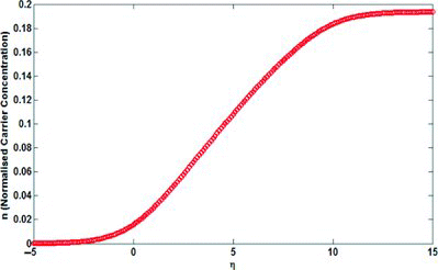
Figure 3. Carrier concentration as a function of normalised Fermi energy.
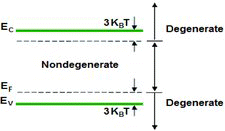
As shown in Figure , if the Fermi level lies in the band gap more than 3KBT from either the conduction or valence band edge where (E − EF) ≥ 3KBT, the cited position of the Fermi level is named non-degenerate region. Conversely, in the degenerate region, the Fermi level is within 3KBT of either band edge or lies inside a band. It should be noted that in the non-degenerate region, the energy states are mostly empty of electrons and f(E) = exp((EF − E)/KBT), while in the degenerate region, the energy states are mostly filled with electrons and the Fermi-Dirac distribution function can be approximated by 1 (f(E) = 1) [Citation38].
Figure 4. Definition of the degenerate and non-degenerate region.
Therefore, Fermi level with the distance more than from either the conduction or valence band edge within the band gap illustrates a non-degenerate condition, which is performed by Equation (13). In case of a non-degenerate region, we can neglect 1 (in the denominator) in comparison with an exponential function because of high difference between x and
[Citation37],
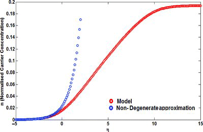
(13) On the other hand, the presented carrier concentration model can be approximated by non-degenerate approximation particularly in lower numbers of
. Also the effect of normalised Fermi energy (η) on a non-degenerate limit as a remarkable parameter is reported. Similar to the conventional 1D device, the carrier concentration indicates a normalised Fermi energy dependence effect for electron concentration as shown in Figure .
Figure 5. The comparison between the presented model and non-degenerate approximation.
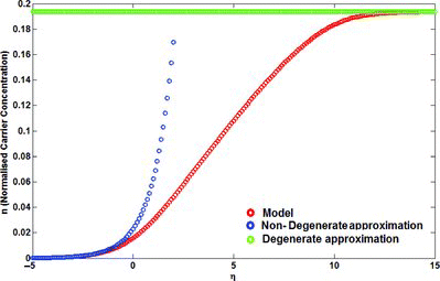
In terms of a semiconductor, in case the Fermi level is situated less than far away from the conduction and valence band, or located within a band, degenerate approximation will play an important role on carrier statistics study. In this regime,
in comparison with 1 can be neglected, because the amount of
is very small [Citation37]. Therefore, we can rewrite the carrier concentration for degenerate region (
) as
(14) As shown in Figure , the presented model is approximated by degenerate approximation, particularly in higher numbers of
. The figure also indicates that ABA-stacked TGN carrier concentration in the degenerate limit is strongly unassociated with the normalised Fermi energy.
Figure 6. The comparison between the presented model, non-degenerate and degenerate approximations.
To get a greater insight into the carrier concentration of TGN FET-based devices, the proposed model is compared with reported data. An analytical modelling of carrier concentration for 1D monolayer GNR [Citation39], 1D BGN [Citation40] and 2D bilayer graphene [Citation41] has been studied theoretically. By comparing the presented model with other types of graphene, it can be stated that the carrier concentration of 1D monolayer GNR is about 105 m−2 in the non-degenerate regime, while it is saturated about 103.5 m−2 in the degenerate regime [Citation39]. Also, comparison study between our model with carrier concentration model of 1D BGN indicates that the amount of concentration for 1D BGN is about 6107 m−2 and 1
107 m−2 in the non-degenerate and degenerate approximations, respectively [Citation40]. The effect of the applied voltage on the carrier concentration model has also been investigated for 2D bilayer graphene [Citation41]. It can be stated that the concentration of carriers rises substantially as the applied voltage is increased from 0.1 eV to 0.9 eV. For an applied voltage of 0.1 eV, the carrier concentration is about 0.5
1017 m−2. In the applied voltage of 0.37 eV, the concentration of carriers has improved to about 1
1017 m−2. Increasing the applied voltage to 0.63 eV and 0.9 eV resulted in the carrier concentration to increase by about 1.5
1017 m−2 and 2.1
1017 m−2, respectively. These researches also indicate that by using the numerical method for non-parabolic band structure of 1D monolayer GNR and BGN in the degenerate limit, carrier concentration strongly depends on normalised Fermi energy and independent on temperature. In the contrary, this model illustrates exponential function of normalised Fermi energy clarifies carrier concentration in low carrier regime. In other words, in non-degenerate regime, carrier concentration of BGNs is a function of temperature particularly in lower number values of concentration. It is predicted that by varying carrier concentration of proposed model, I–V characteristic of TGN FET-based devices can be controlled.
According to Moore's law, the number of transistors per square inch on integrated circuits doubles approximately every two years. It is noteworthy that the capabilities of many digital electronic devices such as processing speed, memory capacity, sensors and even the number and size of pixels in digital cameras are strongly linked to Moore's law [Citation42]. All of these are improving at exponential rates as well, which has dramatically enhanced the impact of digital electronics in nearly every segment of the world economy. In future, nanoelectronic devices will be scaled down to nanoscale size to meet Moore's law, and therefore, will operate in the degenerate limit, which makes the degenerate approximation more dominant in the future nanoscale device modelling. As a result, the developed model can assist in comprehending experiments involving TGN FETs.
5. Conclusion
The focus of this study is to present a new model for TGN carrier concentration. Based on the simulated results, the proposed model can be approximated by the degenerate and non-degenerate approximation in some numbers of normalised Fermi energy. Our results indicate that carrier concentration in the non-degenerate limit is a function of normalised Fermi energy; however, in degenerate limit, it is strongly independent of normalised Fermi energy. The comparison between carrier concentration of TGN with other types of graphene is also done to validate our presented model. By considering outcome from simulations, one can achieve a deeper understanding into device operations and its reliance on the material and geometrical parameters. It can be concluded that the carrier concentration model can be adopted to derive current–voltage characteristic of the nanoelectronic devices. It can also be applied as a useful tool to optimise the TGN FET-based device performance. As a result, TGN FET-based devices can be employed for the future nanoelectronic applications in advancing the technology onward.
Acknowledgements
The authors would like to acknowledge the financial support from Research University grant of the Ministry of Higher Education (MOHE), Malaysia under Projects Q.J130000.7123.02H24, PY/2012/00168 and Q.J130000.7123.02H04. Also, thanks to the Research Management Center (RMC) of University Teknologi Malaysia (UTM) for providing excellent research environment in which to complete this work.
References
- Zebrev GI. Graphene nanoelectronics: electrostatics and kinetics, Micro. Nanoelectron. 2008;7025:M250–M250.
- Ahmadi MT, Rahmani M, Ghadiry MH, Ismail R. Monolayer graphene nanoribbon homojunction characteristics. Sci Adv Mater. 2012;4:1–4.
- Ahmadi MT, Riyadi MA, Saad I, Ismail R.Numerical study of Fermi energy for p-type silicon nanowire. J Nanosci Nanotechnol. 2009;1136:98–102.
- Lemme MC, Echtermeyer TJ, Baus M, Kurz H. A graphene field-effect devices. Electr. Device. L. 2007;28:282–284.
- Ahmadi MT, Michael LP, Ismail R, Arora VK. The high-field drift velocity in degenerately-doped silicon nanowires, Int J Nanotechnol. 2009;6:601–617.
- Rahmani M, Ahmadi MT, Ismail R, Ghadiry MH. Performance of bilayer graphene nanoribbon schottky diode in comparison with conventional diodes. J Comput Theor Nanosci. 2013;10:1–5.
- Rahmani M, Ahmadi MT, Karimi H, Kiani MJ, Akbari E, Ismail R. Analytical modeling of monolayer graphene-based NO2 sensor. Sens Lett. 2012;
- Dragoman M, Dragoman D. Graphene-based quantum electronics. Quantum Electron. 2009;33:165–214.
- Shiro Entani SS, Matsumoto Y, Naramoto H, Hao T, Maeda Y. Interface properties of metal/graphene heterostructures studied by micro-raman spectroscopy. J Phys Chem C. 2010;114:20042–20048.
- Zhang YT, Jiang H, Sun QF, Xie XC. Spin polarization and giant magnetoresistance effect induced by magnetization in zigzag graphene nanoribbons. Phys Rev B. 2010;81:165404.
- Castro Neto AH, Guinea F, Peres NMR, Novoselov KS, Geim AK. The electronic properties of graphene. Rev Mod Phys. 2009;81:109–162.
- Ahmadi MT, Johari Z, Aziziah, Amin NA, Zainal N, Ismail R. Band energy effect on carrier velocity limit in graphene nanoribbon. J Exp Nanosci. 2010;7:62–73.
- Bolotin KI, Sikes KJ, Jiang Z, Klima M, Fudenberg G, Hone J, Kim P, Stormer HL. Ultrahigh electron mobility in suspended graphene. Solid State Commun. 2008;146:351–355.
- Novoselov KS, Geim AK, Morozov SV, Jiang D, Zhang Y, Dubonos SV, Grigorieva IV, Firsov AA. Field effect in atomically thin carbon films. Science. 2004;306:666–669.
- Liang G, Neophytou N, Nikonov DE, Lundstrom MS. Performance projections for ballistic graphene nanoribbon field-effect transistors. IEEE Trans Electron Devices. 2007;54:677–682.
- Obradovic B, Kotlyar R, Heinz F, Matagne P, Rakshit T, Giles MD, Stettler MA, Nikonov DE. Analysis of graphene nanoribbons as a channel material for field-effect transistors, Appl Phys Lett. 2006;88.
- Rahmani M, Ahmadi MT, Kiani MJ, Ismail R. Monolayer graphene nanoribbon pn junction. J Nanoengineer Nanomanufactur. 2010;2:1–4.
- Avetisyan AA, Partoens B, Peeters FM. Stacking order dependent electric field tuning of the band gap in graphene multilayers. Phys Rev B. 2010;81:115432.
- Hass J, de Heer WA, Conrad EH. The growth and morphology of epitaxial multilayer graphene. J Phys-Condens Matter. 2008;20: 323202.
- Terronesa M, Botello-Méndezb A, Delgadoc JC. Graphene and graphite nanoribbons: morphology, properties, synthesis, defects and applications. Nano Today. 2010;5:351–372.
- Koshino M, McCann E. Parity and valley degeneracy in multilayer graphene. Phys Rev B. 2010;81:
- Guinea F, Castro Neto AH, Peres NMR. Interaction effects in single layer and multi-layer graphene. Eur Phys J-Spec Topics. 2007;148:117–125.
- Yuan S, Raedt HD, Katsnelson MI. Electronic transport in disordered bilayer and trilayer graphene. Phys Rev B. 2010;82:235409.
- Aoki M, Amawashi H. Dependence of band structures on stacking and field in layered graphene. Solid State Commun. 2007;142:123–127.
- Koshino M. Interlayer screening effect in graphene multilayers with ABA and ABC stacking. Phys Rev B. 2010;81:125304.
- Zhang F, Sahu B, Min H, MacDonald AH. Band structure of ABC-stacked graphene trilayers. Phys Rev B. 2010;82:035409.
- Craciun MF, Russo S, Yamamoto M, Tarucha S. Tuneable electronic properties in graphene. Nano Today Press. 2011;6:42–60.
- Appenzeller J, Sui Y, Chen ZH. Graphene nanostructures for device applications, Symposium on Vlsi Technology, Digest of Technical Papers. Honolulu, HI, 2009;124–126.
- Koshino M, McCann E. Gate-induced interlayer asymmetry in ABA-stacked trilayer graphene, Phys Rev B. 2009;79:125443.
- Chang CP, Lu CL, Shyu FL, Chen RB, Huang YC, Lin MF. Magnetoelectronic properties of the AB-stacked graphite. Carbon. 2005;43:1424–1431.
- Leenaerts O. An ab initio study of the adsorption of atoms and molecules graphene. Universiti Antwerpen te verdedigen door Antwerpen, Belgium 2010.
- Datta S. Quantum Transport: Atom to Transistor. New York: Cambridge University Press. 2005. p. 113–114.
- Ahmadi MT, Tan LP, Ismail R, Arora VK. The high-field drift velocity in degenerately-doped silicon nanowires. Nanotechnology. 2009;6:601–617.
- Guinea F, Castro Neto AH, Peres NMR. Electronic states and Landau levels in graphene stacks. Phys. Rev. B. 2006;73:245426.
- Rahmani M, Ahmadi MT, Ghadiry MH, Anwar S, Ismail R. The effect of applied voltage on the carrier effective mass in ABA trilayer graphene nanoribbon. J Comput Theoret Nanosci. 2012;9:1618–1621.
- Arora VK. Failure of Ohm's law: its implications on the design of nanoelectronic devices and circuits. Proc IEEE Int Conf Microelectron. 2006;14:15–22.
- Rahmani M. In : Ismail R, Ahmadi MT and Anwar S, editors. Advanced Nanoelectronics. Chapter 8; Trilayer Graphene Nanoribbon Field Effect Transistor Modeling, Boca Raton: Taylor & Francis. 2010; p. 207--237.
- Amin NA, Ahmadi MT, Johari Z, Mousavi SM, Ismail R. Effective mobility model of graphene nanoribbon in parabolic band energy. Mod Phys Lett B. 2011;25:739–745.
- Johari Z, Ahmdi MT, Chang DC, Yih, Amin NA, Ismail R. Modelling of graphene nanoribbon fermi energy. J Nanomater. 2010:6.
- Mousavi SM, Ahmadi MT, Sadeghi H, Nilghaz A, Amin A, Johari Z, Ismail R. Bilayer graphene nanoribbon carrier statistic in degenerate and non degenerate limit. J Comput Theor Nanosci. 2011;8:2029–2032.
- Saeidmanesh M, Ismail R, Ahmadi MT, Ghadiry MH, Akbari E. Perpendicular electric field effect on bilayer graphene carrier statistic. J Comput Theor Nanosci, forthcoming.
- Moor Gordon E. Cramming more components onto integrated circuits. Electronics. 1965; 86:82--85.