Abstract
We present a short review of alloying in uncapped self-organized semiconductor heteronanostructures. Our aim is to provide a logical guide through the main concepts proposed in recent scientific debates. In particular, we focus on the issue of mapping the chemical composition within individual germanium quantum dots grown on silicon surfaces, a widely studied model system with high technological potential. We discuss the different experimental results reported so far in the literature, along with the main theories suggested for their rationalization. In particular, we expand on the interplay of competing factors, including thermodynamic considerations, strain relaxation and kinetic limitations. Finally, we propose a possible pathway towards a unifying picture, with the intention to motivate further research on this topic.
1. Introduction
The spectral properties of ‘natural’ atoms stem from the confinement of electrons in the potential defined by a positively charged nucleus, which can be ultimately pictured as a trap for electrons. Likewise, quantized states may be obtained by designing artificial traps, e.g. by confining charge carriers within three-dimensional quantum boxes. When the size of the latter becomes smaller than the de Broglie wavelength of the carriers (typically 5–100 nm), the splitting of the energy levels might be significantly larger than the thermal energy. Such boxes are usually referred to as Quantum Dots (QDs), and identify a pathway towards the realization of artificial atoms. In principle, if one could achieve complete control over the size and shape of the potential wells enclosing these quantum boxes, electronic energy levels and orbital symmetries could be engineered with large flexibility Citation1 Citation2. Moreover, by adjusting the relative positions within systems of QDs, artificial molecules Citation3 and artificial crystals Citation4 could be designed without restriction. This would open novel ground-breaking horizons at the intersection of physics and materials science and engineering Citation5, Citation6.
The potential of artificial atoms, molecules and crystals for applications is enormous and hardly predictable at present. Fields that could be critically affected include, e.g. lasers, single-photon sources and novel computation technologies. These are only a few important examples where progress would be highly beneficial. QDs may emit light as a result of a stimulated inversion of population and relaxation of the charge carriers’ discrete energy levels. Several reasons motivate research in this field. QD-based lasers are expected to exhibit improved performance with respect to bulk-active emitting materials: a lower threshold power and higher differential gain, a weaker temperature dependence, and primarily a virtually unlimited choice for the output frequency Citation7. Moreover, as will be seen in the following, QDs hold the promise of being compatible with the existing Si-processing technology and therefore allowing the integration of micro- and optoelectronic components on the same wafers. QDs also appear as a viable means for the realization of single-photon sources. Such devices are at the basis of many novel applications proposed in the fields of photonics and quantum computation Citation8 and communication Citation9. Light emission from a single QD would overcome the limitations of present photon sources and enable the generation of highly correlated single photons Citation10. Calculations may be performed by manipulating the electron occupancy and charge transfer in suitable architectures of QDs. Following binary logics, QD-Cellular Automata (QCA) would offer outstanding advantages with respect to transistor-based technology, including improved performance with ongoing miniaturization, parallel computation and adiabatic operation Citation11, Citation12. An even more radical enhancement in the computational power could be obtained by taking advantage of the quantum nature of QDs Citation13. By encoding the logical values ‘0’ and ‘1’ in genuine quantum states (charge states, spin states, etc.) and exploiting their coherent evolution, a new type of information processing would become accessible. This would result in an exponential computational speed-up over classical machines and the possibility of solving a new class of fundamental problems (e.g. factoring large numbers Citation14).
The list of potential applications spans many technological fields, where the introduction of novel and versatile materials, with properties tunable down to the atomic scale, would be particularly useful. Nonetheless we also insist on the great interest of QDs from a fundamental viewpoint. Because of their nature and the challenges related to their fabrication, QDs deserve a thorough analysis that could lead to significant insight on fundamental issues in quantum mechanics and more generally in materials science.
Although there exist many different possibilities for trapping electrical charges within nanosized objects, here we will just expand on one possible scheme. In our example the confining potential barriers are associated with the band alignment in a semiconductor heterostructure composed of a small volume of one material epitaxially embedded within a matrix of another. The chemical inhomogeneity and strain fields may result either in a straddling or in a staggered band alignment Citation15. Under these conditions electrons and holes can be trapped within or close to the embedded volume, which thus acts as a QD.
So far we have not addressed the issue of fabricating QDs. In this work we will focus on a promising bottom-up strategy that could lead to the parallel production of a high surface density of QDs. It relies on the self-organization of nanostructures in specific heteroepitaxial growth processes. The epitaxy of moderately lattice-mismatched semiconductor materials often follows the Stranski–Krastanov (SK) mode (noticeable examples include: Ge/Si, ∼4% lattice mismatch; InAs/GaAs, ∼7%; GaP/GaAs, ∼4%; GaAs/GaSb, ∼7%; AlP/InP, ∼7%; PbSe/PbTe, ∼5%). Two distinct regimes are successively met during the growth of the deposited material on top of the substrate material. Initially a wetting layer (WL) develops as a two-dimensional film, up to a critical thickness, which depends on how the involved materials interact as well as on kinetic conditions. Afterwards, nucleation and growth of three-dimensional islands takes place, mainly driven by a partial release of the strain energy. These islands represent optimal QD candidates. They can be embedded within the host matrix in a subsequent step by further deposition of the substrate material. This would ultimately result in the QD configuration sketched above. A variety of advantages are associated with this technique for QD fabrication: besides the aforementioned intrinsically parallel nature of the process, this approach allows us to achieve very low defect densities, which is a fundamental requirement for QD performance Citation16. Moreover, QDs of very small sizes can be obtained, hopefully resulting in devices operational up to room temperature. Recently it has also been shown that by employing substrates that are structured on the nanometre scale, it becomes possible to obtain regularly positioned arrays of QDs Citation4, Citation17, thus overcoming the drawback of the poor spatial coordination within typical ensembles of self-organized nanostructures Citation18, Citation19.
The position of the discrete energy levels in the QDs depends on the intervening potential barriers, i.e. (for SK-grown quantum dots) on their size and shape, on their chemical composition and on the strain fields in the embedded islands and the surrounding host material. In the absence of defects, strain is inherently bound to the local elemental configuration and elastic properties of the component materials. Consequently, the chemical composition profiles ultimately determine the optoelectronic behaviour of QDs. Hence their thorough characterization is paramount for understanding the artificial atom-like properties of these nanostructures. Some degree of alloying always occurs in SK QDs, even when these are formed by deposition of a nominally elementally pure material. Both the substrate and the deposited atoms can diffuse through the surface and interface regions and eventually become incorporated within the islands. This in principle can occur both during and after deposition.
A wealth of experimental techniques has been adapted to tackle these problems, including combinations of microscopic, spectroscopic and diffractive tools, occasionally with the support of chemical treatment. Spatially resolving experimental probes allow us in principle to access the nanoscale spectroscopically, which basically yields direct elemental information. Among the most promising tools we mention the transmission or scanning electron microscope combined with electron energy loss spectroscopy or energy dispersive X-ray analysis (TEM or SEM with EELS or EDX) Citation20–22, scanning Auger microscopy (SAM), anomalous X-ray diffraction (AXRD) Citation23 and X-ray photoemission electron microscopy (XPEEM) (also operated to inspect the near edge X-ray absorption fine structure – NEXAFS) Citation24–27. Other approaches relate local lattice distortions to the composition-dependent strain gradients in the system. Following this idea the detailed chemical profile in the heterostructures has been inferred from atomically resolved geometrical inhomogeneities. Interesting results have been achieved by cross-sectional scanning tunnelling microscopy (XSTM) Citation28–30 or X-ray diffraction (XRD) mapping Citation31. A very promising approach is based on the selective chemical etching of the samples followed by surface imaging (e.g. by atomic force microscopy – AFM) Citation32–35). Here surface micrographs are compared upon removal of layers at a given stoichiometry, thus allowing us to trace spatially resolved isocompositional contours. Despite the variety of approaches, most of them suffer from severe drawbacks that result in controversial data interpretation or troublesome data acquisition. In some cases the information on single nanostructures is deduced from average properties within a statistical ensemble, as in the case of diffraction-related techniques. Sample preparation and probing procedures are often highly intrusive and significantly alter surface properties, e.g. when producing cross-sectional specimens for TEM or XSTM analysis. Certain experimental tools require prohibitive acquisition times, as in the case of scanning methods such as EELS–EDX/SEM or the SAM. Aside from these technical issues, one common problem consists in disentangling or simply understanding the relationships between chemical content and strain fields. This is particularly noticeable for those methods that rely on a strain measurement to retrieve the local stoichiometry, like XSTM or XRD mapping. Nonetheless to some extent strain also affects both the micro-spectroscopic tools (where it may modify the implicated cross-sections), and the chemical etching procedures (where it might modulate the etch rates).
The scenario seems to be even more challenging from the theoretical viewpoint. As we will see, the systems under analysis are too complex at present for a thorough theoretical description. Intermixing should be modelled within the out-of-equilibrium framework imposed by the growth and subsequent relaxation. In particular, any consistent representation of alloying should regard island composition as determined by processes happening while the island is forming, growing and evolving. As a consequence, a rigorous treatment of intermixing is actually equivalent to a microscopic description of the island growth. Approaches involving the ab initio determination of the relevant adsorption energies and potential barriers for diffusion should self-consistently account for the dependence on strain, reconstruction and local atomic environment. This appears, nowadays, to be impracticable. Attempts to attack this problem with computationally more tractable Monte Carlo (MC) methods have been pursued, and will be briefly described in the following. Nevertheless, these treatments generally require the introduction of a certain number of ad hoc premises, and often miss the kinetic pathways. The most convincing and comprehensive model descriptions follow from qualitative considerations and coarse balances between thermodynamic and kinetic elements.
This review aims at giving an overview of the characterization and modelling of the chemical composition within single nanostructures. We will mainly treat the composition of free-standing (i.e. uncapped) SK islands. The embedding process needed to transform these islands into actual QDs is associated with additional alloying phenomena that further complicate data interpretation. Since the capping process itself is still not fully understood, we prefer to focus on the relationships between the SK grown islands and their chemical profile. Moreover, we will limit our discussion to germanium–silicon surfaces, which represent model systems on account of their relative simplicity. Some of the qualitative considerations in this paper, however, may relate to similar QD systems, e.g. III–V or II–VI compounds. Nonetheless we note that in such cases more complex dynamics can occur, particularly in the presence of compounds featuring interatomic bonds with polar or ionic components, such as, e.g. most functional oxide semiconductors Citation36, Citation37. Moreover, we will primarily focus on the growth resulting from the simple physical vapour deposition (mainly molecular beam epitaxy) of one deposited species (Ge) on a heterosubstrate (Si), where the epitaxial dynamics is essentially controlled by the kinetic conditions dictated by total coverage, growth rate and temperature. Strikingly different morphologies and compositions can be obtained, e.g. with complex chemical vapour deposition procedures Citation38, or by the interplay of surfactants and catalysts Citation39, Citation40. In the following, we will show how the competition between thermodynamic factors and kinetic limitations is precisely the focus of the debate on intermixing in semiconductor QDs. Unfortunately, a precise determination of these two aspects in highly strained nanostructures is almost experimentally inaccessible and theoretically unquantifiable. Nonetheless, we will demonstrate that the experimental ability to map the chemical composition at the nanoscale helps to shed some light on the main microscopic processes that govern the alloying.
In this article, we will review different experimental results and model descriptions of alloying within semiconductor nanostructures, with particular emphasis on the Ge–Si system. Different types of chemical profiles have been measured and substantially incompatible theoretical pictures have been proposed for their description. Here, we will separately analyse the two main classes of experimental results and critically discuss the corresponding theoretical models. After a general introduction on the effects of strain and intermixing in SK heteroepitaxial growth (section 2), we present in section 3 the first class of experimental results characterized by SK islands with highly intermixed centres. The quasi-equilibrium thermodynamic models that have been developed for their description are presented in section 4 and critically confronted in section 5 with the kinetic constraints imposed by the actual growth temperatures. Section 6 analyses the second class of experimentally reported island compositions, marked by highly intermixed corners and edges. In the following two sections, we present alternative theoretical descriptions based on the hypothesis that alloying is mainly caused by surface transport phenomena. In particular, in section 8, we show that a simple kinetic model of the island growth accounts for the essential features of the different experimental composition profiles reported so far in the literature. Section 9 concludes the review, also describing perspectives for future work and developments in the field.
2. Strain relaxation
2.1. Strain relaxation in heteroepitaxial flat layers
To examine the possible thermodynamic factors that prompt intermixing, it is instructive to consider the very fundamentals of the SK growth mode. We start by considering the growth of a ‘film’, which might either be flat or consist of three-dimensional (3D) islands, on a substrate near thermodynamic equilibrium. We choose this approach since its description is both theoretically handy and intuitively enlightening.
Planar growth versus three-dimensional islanding can be rationalized by following the approach introduced by E. Bauer half a century ago Citation41. Layer-by-layer growth of a film composed by N atomic layers is predicted if:
An expression equivalent to equation (Equation1) can also be written for each atomic layer of the film Citation42, Citation43:
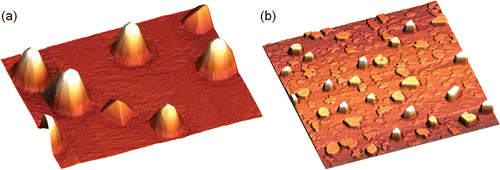
The SK growth mode is distinctive of the heteroepitaxy between materials with a moderate lattice mismatch. The growth of Ge on Si surfaces is a model SK system, where Ge is approximately 4.2% larger than Si. and show examples of typical three-dimensional structures observed on Ge/Si(001) and Ge/Si(111), respectively.
Figure 1. Three-dimensional islands resulting from Stranski–Krastanov growth processes. (a) Pyramid and dome islands obtained by deposition of 0.8 nm of Ge on Si(001) at 560°C (320 × 320 nm2, vertical scale 19 nm, image courtesy of C. Manzano. (b) Strained, intermediate and ripened islands obtained by deposition of 5.4 nm of Ge on Si(111) at 500°C (3 × 3 µm2, vertical scale 29 nm, image courtesy of N. Motta, adapted from Citation44.
A more quantitative treatment of the 2D to 3D morphological transition can be developed by explicitly considering the strain energy induced by the lattice mismatch. Strain and stress can be associated to the elastic properties of the film, i.e. the Poisson number ν and shear modulus μ; to the lattice mismatch between WL and substrate materials, f; and to the overall thickness of the overlayer, t. Under the simplest circumstances of a flat and uniform film, the epitaxial process entails a biaxial stress, which generally results in a tetragonal distortion of the unit cell. By defining the set of coordinates x, y (in plane), z (out of plane), the strain components within the coherent film can be described by the following set of equations:
The surface density of strain energy is thus expected to increase linearly with WL thickness. This can prompt the transition from a flat to a three-dimensional morphology, since – when organized in islands –the film material can relax laterally and assume a more convenient lattice constant. The decrease in strain energy is, however, partially compensated by an increase in surface energy due to the larger surface/volume ratio. As a consequence, the islanding transition can occur only after a given threshold for the elastic energy stored in the film has been exceeded, i.e. according to equation (Equation4), after the WL has attained a given critical thickness. In conclusion, the relaxation of the stress stored in the flat layer provides the thermodynamic driving force towards roughening.
We now examine equation (Equation4) more closely, in particular the implications of the quadratic dependence of the strain energy on the misfit parameter f. In addition to the morphological transition, this hints at another possible pathway towards strain relaxation. A decrease in the lattice mismatch between the substrate and the growing layers would lead to a substantial fall in the strain energy density. In this context intermixing would play a key role. For the epitaxial growth of Ge on Si, this corresponds to the possibility of letting some Si enter the growing film. Under these circumstances the actual average composition of the overlayer would be of the form Si1– x Ge x . An important part of this review will be devoted to a comparison among possible pathways leading to Si–Ge intermixing. For the moment, however, we disregard the way in which this occurs and just suppose that some Si has entered the WL. By assuming that the lattice parameter in the alloy is the average of those of the constituents, weighted by the relevant fractions in the alloy (i.e. according to Vegard's law Citation46), one would conclude that the lattice mismatch between the substrate and alloyed WL is now fx = 0.042x. Hence, if x decreases from unity, the surface density of strain energy decreases accordingly following a quadratic dependence.
The description of alloying in flat layers presented so far is oversimplified. A complete treatment of the problem should consider also the mixing and surface free energies and account for the role of entropy. Nevertheless, these are secondary effects when compared to the relaxation of the strain energy, in particular at the typical temperatures used in growth experiments. Further pathways to strain relaxation emerge when the constraint of perfectly coherent heterostructures is dropped. In this case, the formation of point- and particularly line-like defects of the lattice, as vacancies or interstitials and dislocations, can be very efficient ways of releasing the accumulated strain energy Citation47–49. Here we shall however confine our discussion to the case of strict epitaxial coherence.
2.2. Strain relaxation in three-dimensional islands
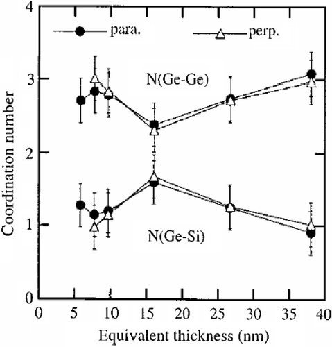
The mechanism of alloying is not an alternative to three-dimensional islanding in the reduction of the strain energy. Actually these two phenomena usually occur simultaneously and are intimately related. Nevertheless, a theoretical description of intermixing in complex three-dimensional structures is significantly more intricate than in planar layers. This is because one should take into account the detailed growth process of SK islands, governed by strongly inhomogeneous strain fields, morphological transitions and kinetic limitations. As a consequence, in order to understand the microscopic processes that cause the alloying of three-dimensional islands, it is necessary to start from the experimental determination of composition and strain profiles. It is nowadays well accepted that alloying in complex SK systems generally occurs and plays an important role. As a noticeable example of the earlier reports on this issue, displays the average coordination numbers measured in GeSi overlayers obtained by deposition of nominally pure Ge on Si(001) substrates. As much as almost 50% silicon (NGe – Ge = 2 and NGe – Si = 2, i.e. one Ge atom bonded to two Ge and two Si atoms on the average) was found to be incorporated within the SK film Citation50.
Figure 2. Average coordination numbers for Ge–Ge and Ge–Si bonds as measured by X-ray absorption spectroscopy. The results are displayed as a function of the amount of Ge deposited on Si(001) at 600°C Citation50. Reprinted with permission from F. Boscherini, G. Capellini, L. Di Gaspare, F. Rosei, N. Motta, S. Mobilio, Appl. Phys. Lett. 76, 682 (2000). Copyright 2000, American Institute of Physics.
In this review, we will primarily focus on the determination of the detailed chemical profiles within individual 3D islands. This topic is presently highly controversial and critical for an understanding of the dynamics governing diffusion and growth in nanostructured surfaces. The experimental reports on the composition of 3D Ge/Si islands can be classified in two almost antithetic main families: (Equation1) those that show a Si-rich core of the islands; and (Equation2) those that describe a Si-enrichment at the islands’ periphery, with centres displaying a lower Si content. As we will see, these kinds of results have been adopted for substantiating conflicting pictures of alloying based on different fundamental processes. In the following, we will discuss in some detail the main results of these two groups of experiments, together with the interpretative efforts that they have spurred. We emphasize here that we do not claim an exhaustive portrait of the existing literature. Rather, we have selected a few representative examples of experimental and theoretical reports and used them to illustrate the logical path in our analysis.
3. Experimental results reporting Si-rich cores
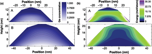
Medeiros-Ribeiro and co-workers have addressed the issue of intermixing within a monomodal distribution of Ge/Si(001) dome islands grown both by chemical vapour deposition (CVD) at 600°C Citation51 and molecular beam epitaxy (MBE) at 700°C Citation23. The data were acquired by a sophisticated combination of AXRD and XRD mapping, which allows them to resolve the detailed three-dimensional stoichiometry within the islands. The nature of the probe leads to the determination of average profiles over large ensembles of nanostructures. However, thanks to the narrow dome size distribution in the investigated samples, these maps can be regarded as representative of the behaviour of individual islands. The result of the analysis is definitely unambiguous, since the average chemical maps feature a few distinct qualitative characteristics. In particular, Si is observed to be mainly incorporated at the core and Ge to segregate towards the surface with a smooth gradation (). The elastic energy maps show a pronounced energy relaxation in correspondence to the higher alloyed regions. Moreover the strain profiles are far from being uniform, with the highest energy values concentrating close to the island base edge ().
Figure 3. (a) Composition maps and (b) corresponding elastic energy maps for Ge dome islands grown on Si(001) by (A) CVD at 600°C, (B) MBE at 700°C (image courtesy of G. Medeiros-Ribeiro, adapted from Citation23)
We note that in these experiments the interpretation of the XRD data is achieved via the assumption of a structural model for the islands. To limit the number of free fitting parameters, a rotational symmetry is frequently assumed. This in turn implies that the final strain and composition maps bear information on the vertical and radial variations only, while possible polar inhomogeneities are averaged out. This is not critical for the dome islands analysed here, which actually display a strong rotational symmetry, but might be important for pyramid islands grown at lower temperatures (see section 6).
Qualitatively similar experimental results (exhibiting highly alloyed nanostructures, especially in the lower and central parts of the islands) have been also obtained by other authors using different experimental techniques Citation50, Citation52–58.
In the original interpretation by Malachias et al . Citation51, although the details of a microscopic pathway are not proposed, a key role is attributed to diffusion during growth. More precisely, a flux of Si atoms would pass through the highly strained lower base of the growing islands during the CVD process, so as to partially release the effective lattice mismatch. The interplay between continuous diffusion and lateral enlargement of the islands would eventually result in the Si-enriched centres. However, several authors have understood the observation of Si-rich cores in particular and of islands with a high degree of Si alloying in general as an indication for the relevance of volume diffusion and stress-driven intermixing processes Citation57, Citation59–63. In these studies the strain energy minimization has been identified as the primary cause in determining the composition profiles. The measured imbalance in the strain energy density (see ) would however suggest that strain gradients are not entirely effective in driving mass exchanges in the system. This simple observation indicates that strain minimization alone cannot uniquely govern the phenomenon, i.e. other factors play an important role. As suggested in the experimental reports we are referring to, these factors might be kinetic in origin and justify the residual strain gradients. Nonetheless we would like to discuss first some of the most significant attempts of rationalizing the Si-rich cores and Ge-rich outer shells through energetic arguments.
4. The thermodynamic model
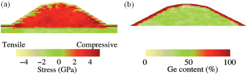
In a picture where thermodynamic factors provide the driving force towards intermixing it is instructive to start by considering the expected strain distribution in a nominally pure island (i.e. composed of 100% Ge) sitting on a nominally pure WL. Different kinds of calculations based either on an atomistic approach Citation60, Citation63–66 or on continuum elasticity theory Citation67 have led to consistent results. The inside of the islands is almost entirely compressed, particularly within a shell in between the core and outer periphery. The strain in the substrate is faintly tensile beneath the island centre, and changes in sign towards a strong compression within a corral below the island perimeter. As an example of the obtained results, represents the z component of the strain tensor below the interface between the Si substrate and the WL underneath a dome (left panel) and a pyramid (right panel) islands.
Figure 4. Computed z component of the strain tensor 2 nm below a sharp Ge–Si interface, in the region under a dome (left panel) and a pyramid (right panel) Citation65. Reprinted with permission from P. Raiteri, L. Miglio, F. Valentinotti, M. Celino, Appl. Phys. Lett. 80, 3736 (2002). Copyright 2002, American Institute of Physics.
This configuration featuring pure Ge islands and WL on top of a pure Si substrate is clearly energetically unfavourable, and almost never experimentally observed if not at extremely low growth temperatures Citation68. Nevertheless, it is used in several theoretical studies as the starting point for an energy minimization process, which is operated via intermixing of the island and substrate materials Citation59–61. Due to the complexity of the system, molecular-dynamics and ab initio calculations are prohibitively time-consuming and therefore not applicable. On the other hand, a combination of atomistic total energy calculations and Monte Carlo methods proved to be most effective for retrieving the thermodynamically favoured configuration. In this process, successive configurations are generated by flipping the elemental identity of randomly chosen neighbouring Ge and Si atoms. After each flip the system is relaxed according to atomistic interaction potentials (typically Tersoff potentials Citation69), with the constraint of a fixed overall geometry Citation59, Citation64. The energy of the new configuration is then calculated, and the Metropolis algorithm is employed to decide whether or not to approve the identity flip. The acceptance of an energetically unfavourable move depends on the thermal budget: the higher the temperature, the easier the consent to the move Citation59. This process is continued until an assigned convergence criterion is met.
The final chemical profiles produced by this simulation approach bear a clear correspondence with the former strain maps: as a rule of thumb the higher the original compression, the larger the Si content. This occurs because the compressive strain field prompts the smaller Si atoms to replace the larger Ge atoms. Thus the cores of the islands become rich in Si while the most superficial layers are rich in Ge. Ge segregation towards island boundaries is further enhanced by the lower surface energy of Ge with respect to Si, and leads to a substantial enthalpy minimization Citation70. This can be only partially compensated by entropy Citation71, Citation72, Citation73, thus typically translating into a Ge-rich external shell in simulations based on thermodynamic equilibration Citation59, Citation74. clearly displays the correspondence between strain and chemical maps. It shows the calculated stressFootnote† (left panel) and composition profiles (right panel) for a dome island before and after relaxing the system by allowing intermixing to occur.
Figure 5. (a) Stress and (b) composition profile of a dome island before and after alloying respectively (adapted from Citation60). Reprinted with permission from G. Hadjisavvas, P.C. Kelires, Phys. Rev. B, 72, 75334 (2005). Copyright 2005 by the American Physical Society.
These quasi-equilibrium models produce compositional profiles that, at least qualitatively, reproduce quite well the experimental results presented in section 3 (for example, compare the right panel of with ). However, also on account of the impossibility to reproduce the composition profiles with Ge-rich cores (see section 6), one should analyse what the implications of these models are, and whether or not these may be consistent with typical experimental conditions.
If the models are to be regarded as a description of the formation process of an island, then they depict a system that evolves in two distinct and temporally subsequent steps: first the islands grow and reach a steady final morphology with a pure Ge composition, and only afterwards relax while preserving their size and shape. Although not representative of the usual experimental conditions, this approach could be realistic for islands first grown at extremely low temperatures, and subsequently processed via a post-growth annealing. However, even in this case, the preservation of the island morphology seems hardly appropriate, given that diffusion processes are supposed to occur. On the other hand, the assumption of an initially pure Ge composition could be regarded simply as the starting configuration for the energy minimization procedure. In this case, the model would not aim at the description of the island evolution, but at pursuing the quasi-equilibrium alloying profile of an island with a given shape Citation61. Nevertheless the viability of this route towards equilibrium is still questionable. The main objections are summarized as follows:
-
The Ge–Si identity flips used in the simulations may represent a feasible microscopic pathway towards alloying only if the associated energy barriers could be readily overcome on time scales comparable to those of a growth experiment.
-
The prescription of a conserved island morphology is actually a strict kinetic limitation Citation59, whose justification becomes quite difficult if, at the same time, bulk interdiffusion is supposed to be thermally activated. Experimental reports have shown that substantial shape and size transformations occur during both growth Citation75–77 and post-growth annealing Citation62, Citation75, Citation76, Citation78.
The first point (i.e. whether bulk atomic exchanges through the islands, the WL and the substrate are ‘kinetically meaningful’) is a most crucial factor in the alloying issue, and represents the very core of the current debate on intermixing in self-organized semiconductor QDs. In the following section, we will try to analyse this point on the basis of the current experimental and theoretical understanding of (inter-) diffusion (in) on Si substrates. Concerning the second point, in section 8.2 we will discuss in some detail the morphological and compositional changes of SiGe/Si(001) islands during post-growth annealing. We will show how such changes can be satisfactorily explained by assuming only surface diffusion processes.
5. Diffusion barriers and kinetic pathways
The motion of atoms, both on the surface and through the bulk, is a thermally activated process, i.e. it is characterized by a hopping rate between neighbouring sites given by an Arrhenius law of the form:
We first consider the case of pure bulk diffusion, i.e. of atomic motion events in regions that are far enough from the surface for their properties to be essentially unaffected by the surface itself. Here, the incorporation of Ge into the Si lattice could be accomplished through two main mechanisms, i.e. either through migration of vacancies or through a process involving the formation of Ge interstitials and the substitution of Ge with Si Citation79. In general, the latter mechanism is thought to dominate the intermixing issue, with fairly high potential barriers of 4–5 eV Citation80. For the temperatures at which Ge/Si QDs are usually grown (between 500 and 700°C) such processes should therefore be considered as practically absent. Since the diffusion of Ge to the very Si bulk is prohibited (which would otherwise lead to a dilute alloy of Ge in Si, at odds with the observed islanding) alloying in QDs must occur through competitive mechanisms.
Within a few atomic layers near the surface, however, the diffusion properties are likely to differ significantly from those of a three-dimensional crystal. This will be particularly enhanced under the strain fields induced by a heteroepitaxial process. It has been suggested that the strain stored during the growth of Ge on Si substrates could significantly increase the atom mobility in the sub-surface region Citation81–85. Some experimental observations indicate that interstitial-mediated interdiffusion could be much faster in the presence of high strain fields, because of an increased flexibility in accommodating interstitials via local deformations of the lattice Citation86. Moreover, there could exist preferential kinetic pathways for Ge in-diffusion inside the Si sub-surface region. Density functional theory (DFT) calculations predict that a Ge atom adsorbed on Si(001) may penetrate into the substrate down to the fifth atomic layer via a specific kinetic pathway composed of interstitials. The corresponding potential barriers would be lower than 2.1 eV Citation87, implying that such processes could indeed be of some relevance in the alloying of islands grown at high temperatures.
Finally, we consider the migration of Si and Ge adatoms at the surface. In the case of Ge/Si(001), both experimental observations Citation88 and ab initio calculations Citation89 agree on energy barriers of ∼0.6–0.7 eV. This would cause such diffusion events to be faster than bulk and sub-surface processes by more than 20 and 8 orders of magnitude, respectively. These figures can be well understood intuitively in terms of the different local coordination numbers (i.e. the number and strength of interatomic bonds that have to be broken and rebuilt during each elementary hopping event).
In conclusion, at the typical growth temperatures of semiconductor QDs, genuine bulk intermixing processes can be safely excluded, sub-surface migration may be relevant, but surface diffusion is to be definitely regarded as the most active process. As a consequence, any realistic description of alloying in QDs should put particular emphasis on the effect of surface diffusion on the island composition. The fact that surface diffusion occurs mainly while the island is forming implies that, as already stated in the introduction, a coherent description of intermixing is necessarily a model of the island growth.
6. Experimental evidence for kinetic limitations: islands with Ge-rich cores
Recent experimental results have demonstrated that, under certain experimental conditions, SK-grown islands can be characterized by compositional maps inconsistent with strain-induced alloying Citation26, Citation33–35, Citation90, Citation91. Ge islands grown on Si substrates were indeed shown to display enhanced intermixing close to their edges and far away from their cores. This would not yield an optimal strain relaxation, and substantially no energetic gain with respect to possible competitive configurations, e.g. to a uniform elemental distribution Citation33. Similar experimental evidence was also reported for capped InGaAs/GaAs(001) islands Citation28–30. This analogy points to some generality in the occurrence of chemical configurations featuring QDs centres enriched in the deposited material, as opposed to highly intermixed peripheries.
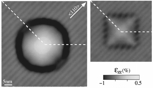
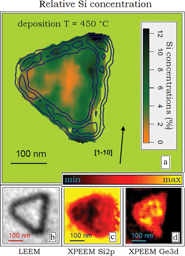
An example of this kind of composition profile in Ge/Si systems was obtained from XPEEM measurements of Ge islands grown on Si(111) by MBE in the temperature range 400–600°C Citation26, Citation27. This technique combines low intrusiveness with excellent elemental sensitivity and allows us to obtain chemical maps of individual islands with a lateral resolution of ∼25 nm Citation92. The experiments consistently revealed a surface stoichiometry with a Si-rich periphery with respect to a Ge-rich centre, though the isocompositional contours exhibited no obvious pattern in the geometrical shape of the islands (). The Si content was measured to increase with the island size and the deposition temperature, with the Si fraction spanning over 10–40% at the edges and only 0–15% at the centres.
Figure 6. (a) Si content at the surface of a typical Ge/Si(111) nanostructure grown at 450°C; (b) low-energy electron microscopy image of the island in (a), displaying its faceted morphology; (c) and (d) relevant Si2p and Ge3d micrographs used for computing (a) Citation26.
Qualitatively similar results were also obtained for pyramid and dome islands grown in the epitaxy of Ge on Si(001), at substrate temperatures between 560 and 600°C Citation33, Citation35. The composition profiles were determined by comparing AFM images of islands prior and following selective wet chemical etching. Since all regions with Ge content higher than 65% are removed by selective etching, this technique directly provides a visual insight into the structure of the Si-rich, and therefore highly intermixed, regions of the islands. The latter were unambiguously shown to be located close to the periphery of the pyramids and domes, leaving characteristic cross- and ring-shaped markers on the surface (see and ).
These composition profiles are clearly not consistent with the thermodynamically stable configurations expected by the quasi-equilibrium models of section 4 Citation59–61. This has prompted some of the authors of these model descriptions to propose that a more complete description of intermixing should include the interplay between strain and kinetic effects. In particular, Hadjisavvas et al . suggested that the introduction of kinetic barriers to diffusion events into a model similar to that illustrated in section 4 may account for the experimental results of and Citation60. The basic idea is that low temperatures and low stress values would prevent the system from reaching the energetically ideal configuration but would still allow for the alloying of the very most strained regions of the islands (i.e. within a shell close to the periphery).
Although such an approach could possibly produce compositional maps with highly intermixed island borders, it is not adequate to account for the Si-rich pyramid corners shown in Citation33, Citation35. Indeed, in a Ge pyramid island regions of high stress are located at the edges rather than at the corners Citation63, Citation93. Moreover, even in their amended version, these thermodynamic models still essentially insist on bulk-like interdiffusion processes for minimizing the thermodynamic potentials. In particular, their formulation ignores any influence of the ‘formation history’ of an island on its final chemical profile. Following the considerations in Section 5, this seems, however, to be fundamental for a correct description of the alloying dynamics under typical experimental conditions.
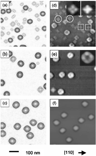
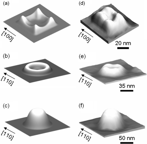
Figure 7. AFM images of Ge/Si(001) samples before (left column) and after (right column) the selective etching process. The growth temperatures are 580°C, 600°C and 620°C for the upper, central and lower row, respectively. The insets show a higher magnification (80 × 80 nm2) of the observed etched morphologies. The two different types of etched pyramids in (d) are attributed to the locally non-uniform distribution and density of the islands Citation35. Reprinted with permission from G. Katsaros, G. Costantini, M. Stoffel, R. Esteban, A.M. Bittner, A. Rastelli, U. Denker, O.G. Schmidt, K. Kern, Phys. Rev. B 72, 195320 (2005). Copyright 2005 by the American Physical Society.
Composition maps with a higher Ge (or InAs) content close to the island centres have on the other hand triggered the development of an alternative conceptual paradigm, where alloying is attributed to surface transport phenomena only (i.e. to a mass transport phenomenon that involves migration of adatoms throughout the topmost atomic layer only). This different class of models is the subject of the next two sections.
7. Alloying through surface diffusion
Neglecting bulk interdiffusion immediately entails that the experimentally observed intermixing does not occur after, but during the growth of the islands, i.e. that morphological and chemical evolutions occur simultaneously. This ultimately corresponds to a scenario where a continuous flux of material of a given composition is adsorbed at the surface of the growing islands. As the growth proceeds, the completion of a surface layer is assumed to ‘freeze’ the motion of any material underneath. In other words, the composition at any interior point of an island is fixed at the time when the point becomes encapsulated inside the island.
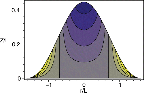
In this section we focus on the limit in which surface diffusion is much faster than the deposition rate Citation28, Citation94, referring to section 8 for the discussion of additional and more stringent kinetic limitations. If the atomic migration is completely activated, the deposited material will be able to diffuse throughout the entire island surface, thoroughly probe the thermodynamic potential, and eventually find the lowest energy configuration, before burial with further deposited material. The incorporation process might however occur in a non-uniform manner because of strain variations across the island surface. Based on these assumptions, Spencer and Blanariu have very recently developed a theoretical description of the growth of small unfaceted Ge islands on Si(001) Citation95. In their model, the morphology and chemistry of the islands are deeply entangled with each other and must be determined self-consistently. While the island shape is computed through the equilibration of the surface chemical potentials, the relevant non-uniform strain fields (due to the detailed island shape) result in a correspondingly non-uniform composition along the surface. As the island grows, the successive burial of these non-uniform surface alloys produces the composition profile depicted in . We note that this model is a refinement of the picture originally developed by Liu et al . for interpreting the compositional maps of capped InGaAs/GaAs(001) QDs Citation28. The results of both models are qualitatively analogous in predicting a peak in Ge (InAs) content located at the central regions and close to the apex of the islands.
Figure 8. Island shape and composition map of an axisymmetric Ge prepyramid on Si(001). Width r, height Z and composition (contour plot) are represented in scaled units. Colour code: bright regions are Si-rich, dark ones are Ge-rich Citation94. Reprinted with permission from B.J. Spencer, M. Blanariu, Phys. Rev. Lett. 95, 206101 (2005). Copyright 2005 by the American Physical Society.
An important issue to be addressed when discussing alloying models where bulk mass transport is neglected is the origin of the substrate material incorporated inside the islands. Indeed, highly intermixed compositional profiles have been measured even for islands grown through deposition of nominally pure material. Models such as those treated in this and the next section assume an influx of substrate atoms stemming from the WL, which is known to be substantially alloyed. These, atoms would access the surface of the islands via diffusion throughout the WL. Thus, the substrate material is not supposed to enter the islands directly, but to reach the WL from the substrate first and the islands from the WL afterwards. However the question about the way the substrate material arrives at the surface of the WL remains unsolved. In the case of Ge/Si(001), it has been proposed that the particular structure of the WL composed of dimer vacancy lines and dimer row vacancies offers preferential channels for the incorporation of Si into the WL during overgrowth Citation95 as well as for the Si out-diffusion during island formation Citation78. This clearly requires a certain degree of activation of bulk-like diffusion, but only through extremely thin and highly strained sub-surface regions (the Ge WL thickness being in between 2 and 3 ML, depending on the substrate temperature Citation96, Citation97) with a particularly porous configuration.
The composition profiles resulting from the simulations in Citation94 and Citation28 agree qualitatively well with most of the experiments reported in section 6, but they cannot reproduce some specific features, such as for example the highly Si-intermixed corners in pyramid islands. A trivial reason for this could be the assumed rotational symmetry in the description of the islands. However a more realistic island morphology alone might not be enough for solving the discrepancy. Indeed these models are still based upon strain energy minimization, which would promote incorporation of Si at the pyramids’ edges more effectively than at the corners Citation63, Citation93. The composition profiles displayed in seem therefore to be the genuine result of kinetic limitations. In the next section, we will discuss what happens when the rejection of bulk interdiffusion is complemented with partial restrictions on surface mobility.
8. Kinetically limited alloying by surface diffusion
8.1. Alloying during growth: a comprehensive model
The last class of theoretical models that we will discuss represents the consequences of the finite diffusion length of atoms at surfaces. For a given substrate this may generally depend upon the elemental identity of the mobile species and the system temperature. With these basic assumptions, a simple kinetic description of the island growth has been developed by Denker et al . Citation33 and extended by Katsaros et al . Citation35, which satisfactorily captures the dependence of the island composition on the main growth parameters: temperature, growth rate, and annealing time.
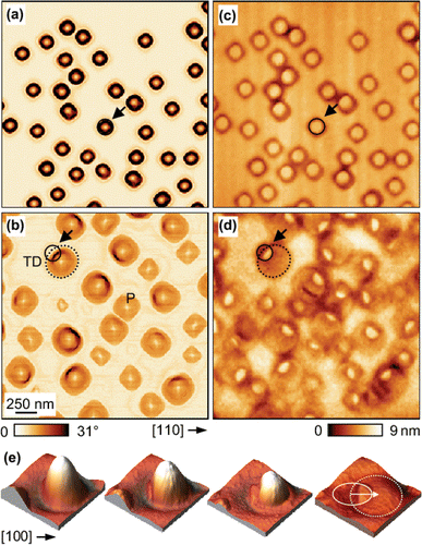
The island growth is simulated through a kinetic MC algorithm, where the islands have a fixed shape and grow by successively adding complete atomic shells (layer-by-layer growth). As in the previous case, the composition at each point of the island is completely determined at the moment of its initial encapsulation. At variance with the models in section 7, however, any effect of the strain energy on the local adsorption probability is neglected. The surface positions where the incoming material becomes incorporated are chosen at random, according to a random walk distribution of atoms starting from the WL (whose composition is fixed at a given Ge x Si1– x stoichiometry). The role of the elemental identity of the diffusing adatoms is projected through a supplementary kinetic constraint: the diffusion length of Ge on the island facets is much longer than that of Si. This assumption has been very recently supported by ab initio calculations predicting a difference of up to three orders of magnitude in the diffusivities of Ge and Si atoms along the {105} facets which enclose pyramid islands Citation98. The results of such simulations for pyramids and domes grown at different temperatures are reported in . The island alloying is mapped through 65% Ge isocompositional profiles, i.e. by displaying all the points of an island with a Ge content lower than 65%. This representation is very convenient for a direct comparison with chemical etching experiments with a Ge over Si selectivity close to 65% Citation33, Citation35. All the observed kinds of compositional maps (either with highly intermixed corners, or peripheries, or centres) can be reproduced, thus demonstrating a remarkable agreement between experiments and simulations.
Figure 9. Simulated (left column) and measured (right column) 65% Ge isocompositional surface profiles of islands grown at increasing substrate temperatures (adapted from Citation35).
In the low-temperature case, consistently with the etching experiments, the simulations produce pyramids with Si-rich corners. This can be described in terms of the interplay of combined effects. Once on the island, Ge atoms can spread evenly over its surface whereas Si atoms, due to their limited diffusivity, linger in the proximities of the borders, where they are eventually buried by the influx of additional material. Because of geometric constraints, the local mass flow rate of WL material reaching the islands is higher at the corners than at the edges. The subsequent net result is indeed a Si-enrichment of the pyramids’ corners. The overall shape of the three-dimensional structures plays a crucial role, as witnessed by the simulated chemical maps inside the domes. When grown at the same temperature as the pyramids, the highly symmetric octagonal base Citation99 of the domes translates into the development of a ring-like Si-rich region ( and ).
Selective etching experiments show that the composition profiles of islands grown at higher temperatures tend to display highly alloyed cores ( and ), in agreement with the reports presented in section 3. This transformation from a Si-rich periphery to a Si-rich centre with the substrate temperature can be consistently captured by the kinetic model by considering both an increased average Si content in the WL Citation100 and a promoted adatom surface diffusivity. In particular, this latter factor implies that Si atoms can move further away from the island borders. This would smear out the inhomogeneities of the resulting alloying profile, as shown in and .
Apparently, this merely kinetic model is adequate for a global description of the issue at hand. It can account for the essential features of the different experimental composition profiles reported so far in the literature. Moreover it provides a qualitative and coherent explanation of the dependence of these profiles on the main growth parameters Citation35. In other words, this paradigm seems to yield at present the best available description of alloying in SK islands. However, the model is evidently based on excessively coarse and oversimplified hypotheses. First and foremost it does not account for the influence of non-uniform strain fields on the adsorption probabilities, which, on the contrary, have to be acknowledged as an important role in the present discussion.
8.2. Alloying during post-growth annealing
Up to now we have discussed the composition of islands on the surface of samples that were quenched to room temperature immediately after interrupting the Ge flux. Before concluding, we want to address the issue of the evolution of islands during post-growth annealing, i.e. an intentional growth interruption at fixed substrate temperature. Several experimental studies have shown the occurrence of a wealth of phenomena, including coarsening, morphological transitions, and further intermixing with the substrate material Citation62, Citation68, Citation75, Citation76, Citation78, Citation101. However, the mechanism leading to further alloying was not clarified until recently.
shows results from a typical annealing experiment where SiGe islands were first grown by deposition of 10 ML of Ge on Si(001) at 740 °C, and then annealed at the same temperature for 20 minutes. The as-grown islands () are bounded by steep facets Citation102 and become larger and shallower upon annealing (). Such a ‘reverse’ morphological transition was previously reported in Citation62, Citation101 and attributed to the strain-relieving effect of alloying. One could imagine that, once islands are formed, further intermixing should proceed through bulk interdiffusion. However, a closer inspection of the samples reveals an intriguing mechanism whereby islands alloy exclusively through surface diffusion.
Figure 10. Representative AFM images of SiGe islands before (a), (b) and after selective removal of the SiGe layer (c), (d) of samples with 10 ML Ge grown at 740°C. In (a), (c) the surface was cooled to room temperature immediately after growth. In (b), (d) the sample was subject to a further annealing for 20 min at 740°C. (e) AFM images (440 × 440 nm2) of a SiGe island annealed for 10 minutes at 740°C (left side) and etched in NH4OH:H2O2 for (from left to right) 80 min, 170 min, and 620 min (adapted from Citation78).
By selectively etching the SiGe material with a HF:H2O2:CH3COOH solution, the islands can be completely removed, thus allowing for a comparison of the substrate below the islands before and after annealing (). Circular Si-plateaus surrounded by deep trenches () are situated underneath the as-grown islands, and correspond to the original island-substrate interface. On the other hand, characteristic ‘half-moon’ structures and larger and shallower trenches are found for the annealed islands. These have been interpreted as resulting from a lateral motion of the islands Citation78. During this movement a part of the initially circular Si-plateau is left uncapped. Here the Si atoms are allowed to migrate away from the compressed region at the foot of the new island edge. Thus only a fraction of the original plateau remains intact, namely the observed ‘half-moons’.
This island motion is accompanied by a substantial alloying process. The lateral displacement can indeed be qualitatively described as due to the transfer of material from one side of the island to the opposite. In particular, the Si atoms removed from the perimeter (trenches and original Si-plateau) are added onto the growing front of the island together with the Ge-rich material of the original island. This ultimately leads to an efficient Si–Ge intermixing process, achieved exclusively via surface diffusion. Therefore, the island size increases while the relevant average Ge fraction decreases. As a result of strain release, steep morphologies become unstable and evolve into shallower shapes.
The alloying can be directly verified by using a different etchant (NH4OH:H2O2) Citation78, Citation103 with a higher selectivity. Annealed islands display an asymmetrical composition. The portion of the islands sitting above the half-moon shaped plateaus is etched faster than the opposite side (). This is consistent with the Ge-richer composition expected for the part of the island which is receding during motion.
As a final remark, we note that the selective removal of the SiGe layer shows that the Si-plateaus are still preserved below the islands after annealing times as long as ten hours. This provides once again indirect evidence that bulk interdiffusion does not play a significant role at the typical temperatures and time scales used for such experiments. (Bulk diffusion would lead to a smearing of the interface between Si substrate and SiGe layer). These results prove how even complex compositional profiles (as revealed by etching; see and Citation35, Citation62, Citation103) can be easily rationalized by invoking genuine surface-mediated diffusion only.
9. Conclusions and outlook
In conclusion, we have presented a short review of the most relevant concepts developed in recent years on the subject of alloying in self-organized semiconductor QDs. These have been illustrated through a critical analysis of both experimental and theoretical reports on the SK epitaxy of germanium on low index silicon surfaces. Very different chemical maps within individual islands have been measured or predicted, thus placing the issue at the centre of a lively debate. Despite the recent progress in the understanding of intermixing dynamics, none of the existing models seems to provide an exhaustive description of the diffusion processes involved in this phenomenon. Nonetheless, nowadays there should be general agreement on a few qualitative principles. Any realistic and consistent model of alloying should aim at reproducing the elemental maps of islands whose chemical and morphological evolutions are correlated deeply and inherently. Indeed the same elementary diffusion processes responsible for the growth of the QDs also govern their concentration profiles. Thus a satisfactory picture of intermixing should be drawn in the form of a growth model, along the lines illustrated in sections 7 and 8 of this article.
Here, we propose a precise path towards the identification of an ideal model description of intermixing. The island growth and evolution is substantially determined by the interplay between thermodynamic equilibration and kinetic constraints. Hence, the explicit account of the competition between deposition rates and temperature-dependent diffusion lengths seems to be the most convenient starting point. On the other hand, energetic factors (primarily strain) should be incorporated via a modulation of the adsorption probability for the diffusing atoms. The real-time evolution of the chemical profiles, geometrical shapes and strain fields during growth should be described self-consistently. The ideal model would be completed by the introduction of bulk-diffusion phenomena, once again within the context of a kinetically limited growth process. This would entail a careful evaluation of the energy barriers for diffusion through the strained volume material, beginning with a thin sub-surface region downwards towards the bulk (which seems beyond reach at the moment).
The roadmap we have identified is certainly ambitious and demanding, yet conceptually well-defined. Moreover, although substantial efforts would still be most desirable, the basic model described in section 8 of this article already provides an excellent zero-order approximation, capable of capturing the essence of the phenomenology reported in the literature. We hope that this brief review will motivate further research towards a refinement of this theoretical picture. Indeed, the achievement of the ideal model description of alloying in semiconductor QDs would stand as a landmark in the ability to control and engineer nanostructures with the desired artificial atom-like behaviour.
Acknowledgements
The authors thank G. Katsaros, S. Kiravittaya, and F. Montalenti for fruitful discussions. F. Rosei acknowledges funding from NSERC (Canada) and FQRNT (Province of Quebec), and is grateful to the Canada Research Chairs program for salary support. F. Ratto is grateful to the International Council of Canadian Studies and FQRNT for graduate fellowships, and the government of Australia for an Endeavour fellowship. We thank N. Motta and G. Medeiros-Ribeiro for providing their original figures, reproduced in this review.
Notes
†It should be noted that, in contrast to the convention adopted in , here negative values correspond to tensile stress.
Related Research Data
References
- Kouwenhoven , L and Marcus , C . 1998 . Quantum dots . Phys. World , 11 : 35
- Petroff , PM , Lorke , A and Imamoglu , A . 2001 . Epitaxially self-assembled quantum dots . Phys. Today , 54 : 46
- Kouwenhoven , L . 1995 . Coupled quantum dots as artificial molecules . Science , 268 : 1440
- Kiravittaya , S , Rastelli , A and Schmidt , OG . 2005 . Self-assembled InAs quantum dots on patterned GaAs(001) substrates: Formation and shape evolution . Appl. Phys. Lett. , 87 : 243112
- Rosei , F . 2004 . Nanostructured surfaces: challenges and frontiers in nanotechnology . J. Phys.: Cond. Matt. , 16 : S1373
- Barth , JV , Costantini , G and Kern , K . 2005 . Engineering atomic and molecular nanostructures at surfaces . Nature , 437 : 671
- Bimberg , D and Ledentsov , N . 2003 . Quantum dots: lasers and amplifiers . J. Phys.: Cond. Matt. , 15 : R1063
- Knill , E , Laflamme , R and Milburn , GJ . 2001 . A scheme for efficient quantum computation with linear optics . Nature , 409 : 46
- Gisin , N , Ribordy , GG , Tittel , W and Zbinden , H . 2002 . Quantum cryptography . Rev. Mod. Phys. , 74 : 145
- Michler , P , Kiraz , A , Becher , C , Schoenfeld , WV , Petroff , PM , Zhang , LD , Hu , E and Imamoglu , A . 2000 . A quantum dot single-photon turnstile device . Science , 290 : 2282
- Lent , CS and Tougaw , PD . 1997 . Device architecture for computing with quantum dots . Proc. IEEE , 85 : 541
- Cole , T and Lusth , JC . 2001 . Quantum-dot cellular automata . Prog. Quantum Electron. , 25 : 165
- Loss , D and DiVincenzo , DP . 1998 . Quantum computation with quantum dots . Phys. Rev. A , 57 : 120
- Shor , PW . 1994 . “ Algorithms for quantum computing: discrete logarithms and factoring ” . In Proceedings of the 35th Annual Symposium on the Foundations of Computer Science , 124 Los Alamos : IEEE Press .
- Yu , PM and Cardona , M . 2004 . Fundamentals of Semiconductors: Physics and Materials Properties , Berlin : Springer .
- Bimberg , D , Grundmann , M and Ledentsov , NN . 1999 . Quantum Dot Heterostructures , Chichester : John Wiley .
- Zhong , ZY and Bauer , G . 2004 . Site-controlled and size-homogeneous Ge islands on prepatterned Si (001) substrates . Appl. Phys. Lett. , 84 : 1922
- Ratto , F , Locatelli , A , Fontana , S , Kharrazi , S , Ashtaputre , S , Kulkarni , SK , Heun , S and Rosei , F . 2006 . Diffusion dynamics during the nucleation and growth of Ge/Si nanostructures on Si(111) . Phys. Rev. Lett. , 96 : 096103
- Schmidt , OG , Kiravittaya , S , Nakamura , Y , Heidemeyer , H , Songmuang , R , Muller , C , Jin-Phillipp , NY , Eberl , K , Wawra , H , Christiansen , S , Grabeldinger , H and Schweizer , H . 2002 . Self-assembled semiconductor nanostructures: climbing up the ladder of order . Surf. Sci. , 514 : 10
- Liao , XZ , Zou , J , Cockayne , DJ , Jiang , ZM , Wang , X and Leon , R . 2000 . Composition and its impact on shape evolution in dislocated Ge(Si)/Si islands . Appl. Phys. Lett. , 77 : 1304
- Zhang , YT , Floyd , M , Driver , KP , Drucker , J , Crozier , PA and Smith , DJ . 2002 . Evolution of Ge/Si(100) island morphology at high temperature . Appl. Phys. Lett. , 80 : 3623
- McDaniel , EP , Jiang , Q , Crozier , PA , Drucker , J and Smith , DJ . 2005 . Kinetic control of Ge(Si)/Si(100) dome cluster composition . Appl. Phys. Lett. , 87 : 223101
- Medeiros-Ribeiro , G , Malachias , A , Kycia , S , Magalhaes-Paniago , R , Kamins , TI and Williams , RS . 2005 . Elastic energy mapping of epitaxial nanocrystals . Appl. Phys. A: Mater. Sci. Process. , 80 : 1211
- Morin , C , Hitchcock , AR , Cornelius , RM , Brash , JL , Urquhart , SG , Scholl , A and Doran , A . 2004 . Selective adsorption of protein on polymer surfaces studied by soft X-ray photoemission electron microscopy . J. Elect. Spectr. & Rel. Phenom. , 137–40 : 785
- Ratto , F , Rosei , F , Locatelli , A , Cherifi , S , Fontana , S , Heun , S , Szkutnik , PD , Sgarlata , A , De Crescenzi , M and Motta , N . 2004 . Composition of Ge(Si) islands in the growth of Ge on Si(111) . Appl. Phys. Lett. , 84 : 4526
- Ratto , F , Locatelli , A , Fontana , S , Kharrazi , S , Ashtaputre , S , Kulkarni , SK , Heun , S and Rosei , F . 2006 . Chemical mapping of individual semiconductor nanostructures . Small , 2 : 401
- Ratto , F , Rosei , F , Locatelli , A , Cherifi , S , Fontana , S , Heun , S , Szkutnik , PD , Sgarlata , A , De Crescenzi , M and Motta , N . 2005 . Composition of Ge(Si) islands in the growth of Ge on Si(111) by x-ray spectromicroscopy . J. Appl. Phys. , 97 : 043516
- Liu , N , Tersoff , J , Baklenov , O , Holmes , AL and Shih , CK . 2000 . Nonuniform composition profile in In0.5Ga0.5As alloy quantum dots . Phys. Rev. Lett. , 84 : 334
- Lenz , A , Timm , R , Eisele , H , Hennig , C , Becker , SK , Sellin , RL , Pohl , UW , Bimberg , D and Dahne , M . 2002 . Reversed truncated cone composition distribution of In0.8Ga0.2As quantum dots overgrown by an In0.1Ga0.9As layer in a GaAs matrix . Appl. Phys. Lett. , 81 : 5150
- Offermans , P , Koenraad , PM , Wolter , JH , Pierz , K , Roy , M and Maksym , PA . 2005 . Atomic-scale structure and photoluminescence of InAs quantum dots in GaAs and AlAs . Phys. Rev. B , 72 : 165332
- Wiebach , T , Schmidbauer , M , Hanke , M , Raidt , H , Kohler , R and Wawra , H . 2000 . Strain and composition in SiGe nanoscale islands studied by x-ray scattering . Phys. Rev. B , 61 : 5571
- Schmidt , OG , Denker , U , Christiansen , S and Ernst , F . 2002 . Composition of self-assembled Ge/Si islands in single and multiple layers . Appl. Phys. Lett. , 81 : 2614
- Denker , U , Stoffel , M and Schmidt , OG . 2003 . Probing the lateral composition profile of self-assembled islands . Phys. Rev. Lett. , 90 : 196102
- Alonso , MI , de la Calle , M , Osso , JO , Garriga , M and Goni , AR . 2005 . Strain and composition profiles of self-assembled Ge/Si(001) islands . J. Appl. Phys. , 98 : 33530
- Katsaros , G , Costantini , G , Stoffel , M , Esteban , R , Bittner , AM , Rastelli , A , Denker , U , Schmidt , OG and Kern , K . 2005 . Kinetic origin of island intermixing during the growth of Ge on Si(001) . Phys. Rev. B , 72 : 195320
- Wang , ZL . 2004 . Functional oxide nanobelts: Materials, properties and potential applications in nanosystems and biotechnology . Ann. Rev. Phys. Chem. , 55 : 159
- Mathur , S , Shen , H , Lecerf , N , Kjekshus , A , Fjellvag , H and Goya , GF . 2002 . Nanocrystalline orthoferrite GdFeO3 from a novel heterobimetallic precursor . Adv. Mater. , 14 : 1405
- Mathur , S , Shen , H , Sivakov , V and Werner , U . 2004 . Germanium nanowires and core-shell nanostructures by chemical vapor deposition of [Ge(C5H5)(2)] . Chem. Mater. , 16 : 2449
- Robinson , JT , Liddle , JA , Minor , A , Radmilovic , V , Yi , DO , Greaney , PA , Long , KN , Chrzan , DC and Dubon , OD . 2005 . Metal-induced assembly of a semiconductor island lattice: Ge truncated pyramids on Au-patterned Si . Nano Lett. , 5 : 2070
- Paul , N , Asaoka , H and Voigtlander , B . 2004 . Comparison between surfactant-mediated Bi/Ge/Si(111) epitaxy and Ge/Si(111) epitaxy . Surf. Sci. , 564 : 187
- Bauer , E . 1958 . Phänomenologische theorie der kristallabscheidung an oberflächen, I-II . Z. Krist. , 110 : 372
- Brune , H and Kern , K . 1997 . The Chemical Physics of Solid Surfaces and Heterogeneous Catalysis , Edited by: Woodruff , DAKaDP . Vol. 8 , 149 Amsterdam : Elsevier .
- Bauer , E and Van der Merwe , JH . 1986 . Structure and growth of crystalline superlattices: From monolayer to superlattice . Phys. Rev. B , 33 : 3657
- Motta , N . 2002 . Self-assembling and ordering of Ge/Si(111) quantum dots: scanning microscopy probe studies . J. Phys.: Cond. Matt. , 14 : 8353
- Tsao , JY . 1993 . Materials Fundamentals of Molecular Beam Epitaxy , San Diego : Academic .
- Denton , AR and Ashcroft , NW . 1991 . Vegard law . Phys. Rev. A , 43 : 3161
- Tersoff , J . 1993 . Dislocations and strain relief in compositionally graded layers . Appl. Phys. Lett. , 62 : 693
- Jesson , DE , Pennycook , SJ , Baribeau , JM and Houghton , DC . 1993 . Direct imaging of surface cusp evolution during strained-layer epitaxy and implications for strain relaxation . Phys. Rev. Lett. , 71 : 1744
- Wedler , G , Walz , J , Hesjedal , T , Chilla , E and Koch , R . 1998 . Stress and relief of misfit strain of Ge/Si(001) . Phys. Rev. Lett. , 80 : 2382
- Boscherini , F , Capellini , G , Di Gaspare , L , Rosei , F , Motta , N and Mobilio , S . 2000 . Ge-Si intermixing in Ge quantum dots on Si(001) and Si(111) . Appl. Phys. Lett. , 76 : 682
- Malachias , A , Kycia , S , Medeiros-Ribeiro , G , Magalhaes-Paniago , R , Kamins , TI and Williams , RS . 2003 . 3D composition of epitaxial nanocrystals by anomalous x-ray diffraction: Observation of a Si-rich core in Ge domes on Si(100) . Phys. Rev. Lett. , 91 : 176101
- Stangl , J , Daniel , A , Holy , V , Roch , T , Bauer , G , Kegel , I , Metzger , TH , Wiebach , T , Schmidt , OG and Eberl , K . 2001 . Strain and composition distribution in uncapped SiGe islands from x-ray diffraction . Appl. Phys. Lett. , 79 : 1474
- Capellini , G , De Seta , M and Evangelisti , F . 2001 . SiGe intermixing in Ge/Si(100) islands . Appl. Phys. Lett. , 78 : 303
- Magalhaes-Paniago , R , Medeiros-Ribeiro , G , Malachias , A , Kycia , S , Kamins , TI and Williams , RS . 2002 . Direct evaluation of composition profile, strain relaxation, and elastic energy of Ge : Si(001) self-assembled islands by anomalous x-ray scattering . Phys. Rev. B , 66 : 245312
- Kolobov , AV , Oyanagi , H , Wei , SQ , Brunner , K , Abstreiter , G and Tanaka , K . 2002 . Local structure of Ge quantum dots self-assembled on Si(100) probed by x-ray absorption fine-structure spectroscopy . Phys. Rev. B , 66 : 75319
- Motta , N , Rosei , F , Sgarlata , A , Capellini , G , Mobilio , S and Boscherini , F . 2002 . Evolution of the intermixing process in Ge/Si(111) self-assembled islands . Mat. Sci. Eng. B , 88 : 264
- Floyd , M , Zhang , YT , Driver , KP , Drucker , J , Crozier , PA and Smith , DJ . 2003 . Nanometer-scale composition measurements of Ge/Si(100) islands . Appl. Phys. Lett. , 82 : 1473
- Schulli , TU , Stoffel , M , Hesse , A , Stangl , J , Lechner , RT , Wintersberger , E , Sztucki , M , Metzger , TH , Schmidt , OG and Bauer , G . 2005 . Influence of growth temperature on interdiffusion in uncapped SiGe-islands on Si(001) determined by anomalous x-ray diffraction and reciprocal space mapping . Phys. Rev. B , 71 : 35326
- Sonnet , P and Kelires , PC . 2002 . Monte Carlo studies of stress fields and intermixing in Ge/Si(100) quantum dots . Phys. Rev. B , 66 : 205307
- Hadjisavvas , G and Kelires , PC . 2005 . Critical aspects of alloying and stress relaxation in Ge/Si(100) islands . Phys. Rev. B , 72 : 75334
- Lang , C , Cockayne , DJH and Nguyen-Manh , D . 2005 . Alloyed Ge(Si)/Si(001) islands: The composition profile and the shape transformation . Phys. Rev. B , 72 : 155328
- Kamins , TI , Medeiros-Ribeiro , G , Ohlberg , DAA and Williams , RS . 1998 . Dome-to-pyramid transition induced by alloying of Ge islands on Si(001) . Appl. Phys. A: Mater. Sci. Process. , 67 : 727
- Chaparro , SA , Drucker , J , Zhang , Y , Chandrasekhar , D , McCartney , MR and Smith , DJ . 1999 . Strain-driven alloying in Ge/Si(100) coherent islands . Phys. Rev. Lett. , 83 : 1199
- Lang , C , Nguyen-Manh , D and Cockayne , DJH . 2003 . Nonuniform alloying in Ge(Si)/Si(001) quantum dots . J. Appl. Phys. , 94 : 7067
- Raiteri , P , Miglio , L , Valentinotti , F and Celino , M . 2002 . Strain maps at the atomic scale below Ge pyramids and domes on a Si substrate . Appl. Phys. Lett. , 80 : 3736
- Yu , WB and Madhukar , A . 1997 . Molecular dynamics study of coherent island energetics, stresses, and strains in highly strained epitaxy (vol 79, pg 905, 1997) . Phys. Rev. Lett. , 79 : 4939
- Spencer , BJ and Tersoff , J . 2001 . Stresses and first-order dislocation energetics in equilibrium Stranski-Krastanow islands . Phys. Rev. B , 63 : 205424
- Denker , U , Sigg , H and Schmidt , OG . 2004 . Intermixing in Ge hut cluster islands . Appl. Surf. Sci. , 224 : 127
- Tersoff , J . 1989 . Modeling solid-state chemistry: Interatomic potentials for multicomponent systems . Phys. Rev. B , 39 : 5566
- Kelires , PC and Tersoff , J . 1989 . Equilibrium alloy properties by direct simulation: Oscillatory segregation at the Si-Ge(100) 2X1 surface . Phys. Rev. Lett. , 63 : 1164
- Wagner , RJ and Gulari , E . 2004 . Simulation of Ge/Si intermixing during heteroepitaxy . Phys. Rev. B , 69 : 195312
- Nurminen , L , Tavazza , F , Landau , DP , Kuronen , A and Kaski , K . 2003 . Reconstruction and intermixing in thin Ge layers on Si(001) . Phys. Rev. B , 68 : 085326
- Cho , JH and Kang , MH . 2000 . Ge-Si intermixing at the Ge/Si(001) surface . Phys. Rev. B , 61 : 1688
- Tarus , J , Tantarimaki , M and Nordlund , K . 2005 . Segregation in SiGe clusters . Nucl. Instr. Meth. Phys. Res. B , 228 : 51
- Ross , FM , Tromp , RM and Reuter , MC . 1999 . Transition states between pyramids and domes during Ge/Si island growth . Science , 286 : 1931
- Montalenti , F , Raiteri , P , Migas , DB , von Kanel , H , Rastelli , A , Manzano , C , Costantini , G , Denker , U , Schmidt , OG , Kern , K and Miglio , L . 2004 . Atomic-scale pathway of the pyramid-to-dome transition during Ge growth on Si(001) . Phys. Rev. Lett. , 93 : 216102
- Rastelli , A , Stoffel , M , Tersoff , J , Kar , GS and Schmidt , OG . 2005 . Kinetic evolution and equilibrium morphology of strained islands . Phys. Rev. Lett. , 95 : 026103
- Denker , U , Rastelli , A , Stoffel , M , Tersoff , J , Katsaros , G , Costantini , G , Kern , K , Jin-Phillipp , NY , Jesson , DE and Schmidt , OG . 2005 . Lateral motion of SiGe islands driven by surface-mediated alloying . Phys. Rev. Lett. , 94 : 216103
- Willoughby , AFW . 1978 . Atomic diffusion in semiconductors . Rep. Prog. Phys. , 41 : 1665
- Sugii , N . 2001 . Thermal stability of the strained-Si/Si0.7Ge0.3 heterostructure . J. Appl. Phys. , 89 : 6459
- Chang , SJ , Wang , KL , Bowman , RC and Adams , PM . 1989 . Interdiffusion in a symmetrically strained Ge/Si superlattice . Appl. Phys. Lett. , 54 : 1253
- Sunamura , H , Fukatsu , S , Usami , N and Shiraki , Y . 1993 . Luminescence study on interdiffusion in strained Si1-XGeX/Si single quantum-wells grown by molecular-beam epitaxy . Appl. Phys. Lett. , 63 : 1651
- Boucaud , P , Wu , L , Guedj , C , Julien , FH , Sajnes , I , Campidelli , Y and Garchery , L . 1996 . Photoluminescence and intersubband absorption spectroscopy of interdiffused Si/SiGe quantum wells . J. Appl. Phys. , 80 : 1414
- Wan , J , Luo , YH , Jiang , ZM , Jin , G , Liu , JL , Wang , KL , Liao , XZ and Zou , J . 2001 . Ge/Si interdiffusion in the GeSi dots and wetting layers . J. Appl. Phys. , 90 : 4290
- Rosei , F and Raiteri , P . 2002 . Stress induced surface melting during the growth of the Ge wetting layer on Si(001) and Si(111) . Appl. Surf. Sci. , 195 : 16
- Aubertine , DB , Mander , MA , Ozguven , N , Marshall , AF , McIntyre , PC , Chu , JO and Mooney , PM . 2002 . Observation and modeling of the initial fast interdiffusion regime in Si/SiGe multilayers . J. Appl. Phys. , 92 : 5027
- Uberuaga , BP , Leskovar , M , Smith , AP , Jonsson , H and Olmstead , M . 2000 . Diffusion of Ge below the Si(100) surface: Theory and experiment . Phys. Rev. Lett. , 84 : 2441
- Mo , YW , Kleiner , J , Webb , MB and Lagally , MG . 1991 . Activation-energy for surface diffusion of Si on Si(001): A Scanning-tunneling-microscopy study . Phys. Rev. Lett. , 66 : 1998
- Milman , V , Jesson , DE , Pennycook , SJ , Payne , MC , Lee , MH and Stich , I . 1994 . Large-scale ab-initio study of the binding and diffusion of a Ge adatom on the Si(100) surface . Phys. Rev. B , 50 : 2663
- Ide , T , Sakai , A and Shimizu , K . 1999 . Nanometer-scale imaging of strain in Ge island on Si(001) surface . Thin Solid Films , 357 : 22
- Xue , F , Qin , J , Cui , J , Fan , YL , Jiang , ZM and Yang , XJ . 2005 . Studying the lateral composition in Ge quantum dots on Si(001) by conductive atomic force microscopy . Surf. Sci. , 592 : 65
- Heun , S , Watanabe , Y , Ressel , B , Bottomley , D , Schmidt , T and Prince , KC . 2001 . Core-level photoelectron spectroscopy from individual heteroepitaxial nanocrystals on GaAs(001) . Phys. Rev. B , 63 : 125335
- Raiteri , P and Miglio , L . (private communication)
- Spencer , BJ and Blanariu , M . 2005 . Shape and composition map of a prepyramid quantum dot . Phys. Rev. Lett. , 95 : 206101
- Rastelli , A , von Känel , H , Albini , G , Raiteri , P , Migas , DB and Miglio , L . 2003 . Morphological and compositional evolution of the Ge/Si(001) surface during exposure to a Si flux . Phys. Rev. Lett. , 90 : 216104
- Kohler , U , Jusko , O , Muller , B , Hornvonhoegen , M and Pook , M . 1992 . Layer-by-layer growth of germanium on Si(100): Strain-induced morphology and the influence of surfactants . Ultramicroscopy , 42 : 832
- Tomitori , M , Watanabe , K , Kobayashi , M and Nishikawa , O . 1994 . STM study of the Ge growth mode on Si(001) substrates . Appl. Surf. Sci. , 76 : 322
- Huang , L , Liu , F , Lu , GH and Gong , XG . 2006 . Surface mobility difference between Si and Ge and its effect on growth of SiGe alloy films and islands . Phys. Rev. Lett. , 96 : 16103
- Rastelli , A and von Känel , H . 2002 . Surface evolution of faceted islands . Surf. Sci. , 515 : L493
- Katsaros , G , Rastelli , A , Stoffel , M , Acosta-Diaz , P , Schmidt , OG , Costantini , G and Kern , K . (in preparation)
- Kamins , TI , Medeiros-Ribeiro , G , Ohlberg , DAA and Williams , RS . 1999 . Evolution of Ge islands on Si(001) during annealing . J. Appl. Phys. , 85 : 1159
- Stoffel , M , Rastelli , A , Merdzhanova , T and Schmidt , OG . (submitted)
- Katsaros , G , Rastelli , A , Stoffel , M , Isella , G , von Kanel , H , Bittner , AM , Tersoff , J , Denker , U , Schmidt , OG , Costantini , G and Kern , K . 2006 . Investigating the lateral motion of SiGe islands by selective chemical etching . Surf. Sci. , 600 : 2606