Abstract
In this paper, we address the effect of plasma nitridation on the gate dielectric in terms of device characteristics of an NMOS/PMOS transistor. Firstly, boron segregation due to plasma nitridation near Si/SiO2 interface and bulk Si is experimentally characterised by 1D SIMS, and its profile is reproduced in simulation of which parameters for boron diffusion are accurately calibrated through a comprehensive calibration process. Secondly, the electrical behaviour of NMOS/PMOS transistor with plasma nitride gate dielectric is verified, observing uncommon behaviour of C-V diagram in the case of buried-channel PMOS transistor. We prove that an excessive amount of interface traps generated by plasma nitridation influence abnormal electrical behaviour of the NMOS/PMOS transistor.
1. Introduction
Plasma nitridation provides strong immunity to boron penetration of p+ poly gate and incorporates nitrogen (N) atoms at the Si/SiO2 interface which improves hot carrier resistance, leakage current and stress immunity. These principal advantages of plasma nitrided gate dielectric over conventional oxynitridation with NO or N2O have motivated much work on its utilisation, and plasma nitridation is now regarded as a promising technology for a reliable gate insulator for electrical erasable nonvolatile memory such as flash memory Citation1, Citation2. However, there remain many issues to be addressed if its electrical characteristics are considered Citation3. One of the issues is the dopant segregation of additional annealing process of plasma nitridation, which changes the electrical property of cells and peripheral transistors. Another problem is the effect of the positive charge trap mainly generated in Si/SiO2 interface where ion damage of plasma nitridation is maximised. In this paper, we address the effect of plasma nitridation on the gate dielectric by combined experimental and simulation study of gate oxidation.
2. Experiments and simulations
Samples needed for this study are fabricated with the same process for the fabrication of 63 nm NAND flash cell transistor Citation4. BF2 dose (7 × 1012cm−2) for NMOS transistor and BF2 dose (1 × 1013cm−2) for PMOS transistor are implanted separately at low energy (20 KeV) through a screen oxide. After the screen oxide removal, gate oxidation is performed to grow 80 A oxide with temperature of 900°C for 60 minutes. Poly-Silicon is used as gate material and aluminum is used for metal electrode.
2.1. Boron segregation
First, boron segregation at the Si/SiO2 interface and boron diffusion in silicon surface are experimentally characterised by means of 1D SIMS. Samples with various gate oxidations are prepared with the same process conditions as listed in . After growing gate dielectric by dry oxidation, NO anneal and plasma nitridation are applied to several samples selectively. Boron segregation acquired by high-resolution 1D SIMS is depicted in . It is seen that the boron concentration profile is changed when NO anneal is added while plasma nitridation has no effect on the profile. Thus, it is confirmed that plasma nitrided gate dielectric possesses the same boron concentration profile on Si as the gate dielectric with dry oxidation.
Figure 1. SIMS profiles for samples with gate oxidation.
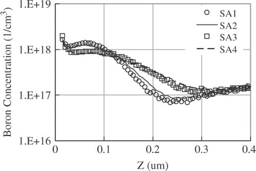
Table 1. Samples used to study segregation during gate oxidation.
2.2. 3-D simulation calibration
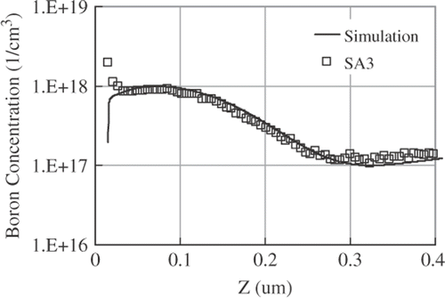
Secondly, a comprehensive process simulation model is accurately calibrated and then exploited to investigate the dependence of device electrical parameters on NMOS/PMOS transistors. As shown in , 2-D and 3-D process simulation are performed with ENEXSS tools and device simulation is performed with Synopsys tools Citation5. For accurate simulation, critical physical dimensions such as length/width of transistor and tunnel oxide thickness are measured by SEM and TEM. To extract process simulation model parameters (boron segregation, oxidation enhanced diffusion (OED) and transient enhanced diffusion (TED)), a variety of NMOS/PMOS transistors with different lengths and widths are tested. After the calibration, we obtained Id-Vg profiles of NMOS/PMOS transistor with different length as shown in . It is seen that ION, IOFF and VTH are correctly simulated on both the length of 0.3 µm and 20 µm. Based on these calibration results, boron concentration profile in Si is constructed as shown in . Since the calibration is performed with typical dry oxidation models while neglecting the effect of plasma nitridation, we compare the boron profile of a SA3 sample for a start. The simulation profile shows a good match to SIMS data in Si, confirming the accuracy of the calibration. Since the 3-D simulation has different material on top of the Si/SiO2 interface, the boron profile near Si/SiO2 the interface is different when compared to SIMS data.
Figure 2. Doping concentration of PMOS transistor constructed by 2-D process simulation.
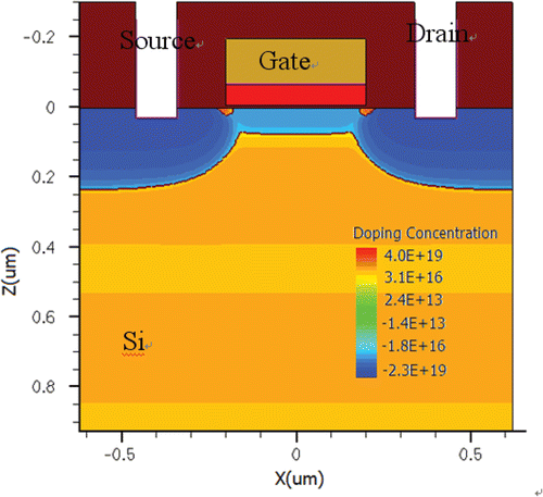
Figure 3. Id-Vg profiles of SA3 (NO annealed gate dielectric) sample for LVN and LVP transistor. Length dependency is shown well fitted due to the calibration of process simulation parameters.
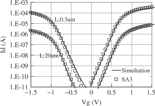
Figure 4. SIMS profile of SA3 sample and calibrated simulation result near Si/SiO2 interface.
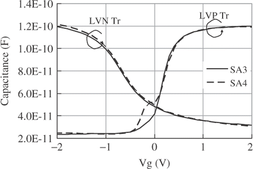
For identifying the electrical characteristics of plasma nitrided gate dielectric, Id-Vg curves for the LVN/LVP transistor are measured experimentally and compared as shown in . While both samples possess the same boron concentration profile in Si, VTH of NMOS and PMOS transistor of plasma nitrided gate oxide is 0.1 V lower than the sample of dry oxidation. Furthermore, in a C-V diagram of each sample as shown in , it is observed that uncommon peak near Vg = 0 V on a buried channel PMOS capacitor exists in the case of plasma nitrided gate dielectric. These results indicate that plasma nitridation alters the physical property in bulk SiO2 and Si/SiO2 surface and changes the electrical characteristics of the NMOS/PMOS transistor.
Figure 5. Id-Vg profiles for LVN and LVP transistor. SA4 sample (plasma nitrided gate dielectric) possesses 0.1 V lower VTH value than SA3 sample.
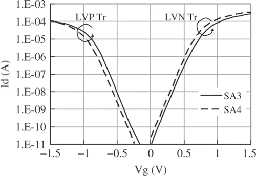
Figure 6. C-V profiles of surface channel NMOS and buried channel PMOS capacitors with different gate oxidation conditions. Buried channel PMOS capacitor of SA4 exhibits uncommon shape near Vg = 0 V.
2.3. C-V diagram of plasma nitrided oxide
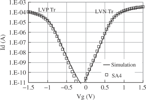
For the purpose of identifying the reason for 0.1 V difference in Id-Vg curve and abnormal peak in C-V diagram, we utilise 3-D simulation. In 3-D simulation, we added several oxide bulk traps and interface traps into the SiO2 and Si/SiO2 interface deliberately, and then observed their device characteristics. As shown in , the C-V curve is reproduced by adding an excessive amount of interface trap in Si/SiO2 interface. The amount of interface trap was measured to be 9e11 which is three times higher than that of dry oxidation. The excessive trap located near interface is regarded as the evidence of positive charge trap of the plasma nitrided gate dielectric Citation1, Citation2. The uncommon peak near Vg = 0 V in the C-V diagram illustrates VTH shift by electron trap/detrap of the trap sites in gate dielectric and appears clearly on the buried channel PMOS capacitor since its C-V curve changes mainly under inversion conditions with abundant supply of electrons from N-Well Citation6, Citation7. Whereas, the surface channel NMOS capacitor shows little change since its C-V curve changes under the depletion condition with few electrons on the Si surface. While oxide bulk trap possesses the same effect on the shift of Id-Vg curve as interface trap, it has no influence on abnormal peak of the C-V diagram. Based on these process and device simulation parameters, Id-Vg characteristics of NMOS and PMOS transistor with plasma nitrided gate dielectric are obtained by the device simulation as shown in . It shows good agreement with experimental data, confirming that 0.1 V VTH shift was attributed by positive charge trap of the plasma nitrided gate dielectric.
Figure 7. C-V profile for buried channel PMOS capacitor with SA4 sample and calibrated simulation result. Nit value equals 9E11 which is three times higher than that of SA3 sample.
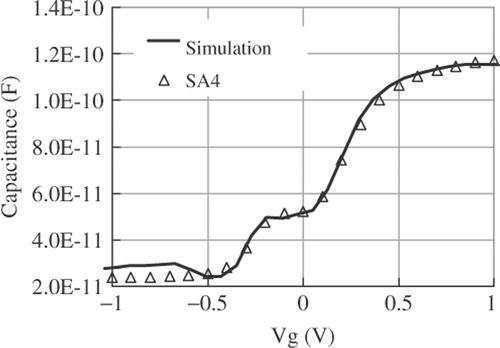
Figure 8. Id-Vg profiles for surface channel NMOS and buried channel PMOS transistor of SA4 sample. Simulation results with NIT value of 9E11 show good agreement with experiments.
3. Conclusions
The effect of plasma nitridation on the gate dielectric in terms of device characteristics is investigated through simulations and experiments. First, based on accurate calibration of 3-D simulation, it is verified that plasma nitridation has no effect on boron segregation near the Si/SiO2 interface and bulk Si. Secondly, we observe uncommon behaviour of the C-V diagram in the case of buried-channel PMOS transistor. We prove that it is due to an excessive amount of interface traps generated by plasma nitridation.
References
- Heo , J , Kim , D , Koo , B , Kim , J , Kim , C , Noh , Y , Baek , S , Shin , Y , Chung , U and Moon , J . 2005 . “ Effects of plasma nitridation on the electrical properties of nitrided oxide gate dielectric for DRAM application ” . In Proceedings of the 35th European Solid-State Device Research Conference 205 – 208 .
- Elnaby , M , Ikeda , A , Hattori , R and Kuroki , Y . 2000 . Effect of nitrogen plasma conditions on the electrical properties of silicon oxynitrided thin films for flash memory applications , 251 – 256 . ICM : in Proceedings of the 12th International Conference on Microelectronics .
- Ghetti , A , Benvenuti , A , Molteni , G , Alberci , S , Soncini , V and Pavan , A . 2004 . “ Electron Devices Meeting ” . In Experimental and simulation study of boron segregation and diffusion during gate oxidation and spike annealing , IEDM Technical Digest, IEEE International 983 – 986 .
- Hur , J-H , Park , S-H , Leex , J-H , Park , J-T , Sel , J-S , Kim , J-W , Song , S-B , Lee , J-Y , Lee , J-H Son , S-J . 2004 . “ 8 Gb MLC (multi-level cell) NAND flash memory using 63 nm process technology ” . In Electron Devices Meeting, IEDM Technical Digest , 873 – 876 . IEEE International .
- Oh , H-S , Lee , S-C , Lee , C-S , Oh , D-Y , Kim , T-K , Song , J-H , Lee , K-H , Park , Y-K , Choi , J-H and Kong , J-T . 2004 . “ 3-dimensional analysis on the cell string current of NAND flash memory ” . In Non-Volatile Memory Technology Symposium Vol. 7 , 137 – 139 .
- White , M , Wiele , F and Lambrot , J . 1980 . High-accuracy MOS models for computer-aided design . IEEE Trans. Electron Devices , 27 : 899 – 906 .
- Tol , MVan der and Chamberlain , S . 1989 . Potential and electron distribution model for the buried-channel MOSFET . IEEE Trans. Electron Devices , 36 : 670 – 688 .