Abstract
The semiconductor industry uses a number of gases classified as perfluorocompounds (PFCs) in both silicon and dielectric layer etching and chamber cleaning in wafer fabrication equipment. The use of PFC gases in these processes is crucial to the production of semiconductor devices, as there are no effective substitutes that can be utilized. Although PFC emissions caused by the semiconductor industry are a tiny fraction of all industry greenhouse gases emissions, the world's semiconductor manufacturers, assembled in the World Semiconductor Council (WSC) and its affiliated associations, have officially agreed to voluntarily reduce atmospheric emissions of PFCs to 10% below baseline levels in 2010. The WSC has established a reporting program to track PFC emissions by the present five semiconductor manufacturing associations (USA, Europe, Japan, Taiwan, Korea). Data released by the WSC today show that the 2008 PFC emissions in most regions are already below the target set for 2010. This cooperative effort by the members of the WSC to reduce PFC emissions is an excellent example of what can be accomplished by collaboration. Because the PFC emission reduction program is considered to be pre-competitive, members freely share information on techniques and strategies. One of the key success factors has also been the strong involvement of equipment and gas suppliers to the semiconductor industry. Key measures that have contributed to substantially reduce PFC emissions are, among others, installation of dedicated post process tool PFC abatement, and application of NF3 gas in combination with so-called remote plasma in chamber cleans. The latter affords a highly efficient process alternative for the semiconductor industry with minimal PFC emission footprint, since the NF3 is utilized with better than 98% conversion efficiency. A gradual trend is visible, i.e. more advanced tools and facilities with relatively low emissions are supplanting relatively old tools and facilities with relatively high emission profiles. Presently, the global semiconductor industry is considering whether and how PFC emissions can be further reduced post-2010. A new global agreement should include other relevant regions with substantial semiconductor production, such as China and Singapore. Such discussions have already commenced. One of the key elements in a new agreement is harmonization of regional reporting. Moreover, it should be emphasized that semiconductor manufacture is no longer the sole or even the largest industry that makes use of PFCs. In this respect, the production of Liquid Crystal Displays (LCDs) and the manufacture of photovoltaic cells are likely to become major players.
1 Policy of the semiconductor industry with respect to global warming by PFCs from the semiconductor industry
1.1 The semiconductor industry
The semiconductor industry features a number of distinct characteristics that position it uniquely in the global economy:
High intensity of R&D spending (up to 20% of annual revenues) and the high level of capital investments for a new semiconductor plant ($2.5–3 billion). | |||||
Semiconductor industry is a technology enabler. Semiconductor products form an increasingly vital part of a whole range of consumer products ranging from electronic devices and systems (e.g. PCs, mobile phones, TV sets) to solutions and services (e.g. Internet providers, telecom operators, broadcasting services, automotive industry). Revenues in the overall microelectronics industry have a multiplier effect on other major downstream sectors where electronic content is central. On a worldwide base the semiconductor market in 2008 is estimated at approximately € 170 billion/US$ 249 billion. | |||||
The European semiconductor market amounted to approximately 15.3% of the world market in 2008. Just like the contributions of the US and Japan, this share is steadily decreasing in favor of the new economies in the Asia-Pacific region. Nevertheless, with its branching into other industry sectors, the semiconductor industry has still remained a key source of employment in the traditional manufacturing areas. | |||||
1.2 PFC uses in the semiconductor industry and their criticality
To produce semiconductor devices, the semiconductor industry requires gaseous fluorinated compounds, silanes, doping and other inorganic gases. Wafers consist of high-purity silicon and are the basic building blocks for all semiconductor components. The PFCs used in semiconductor manufacturing process are: hexafluoroethane (C2F6), octofluoropropane (C3F8), tetrafluoromethane (CF4), octofluorocyclobutane (c-C4F8), nitrogen trifluoride (NF3), sulfur hexafluoride (SF6), and hydrofluorocarbons, such as trifluoromethane (CHF3).
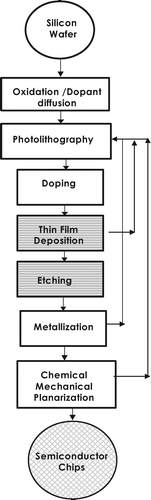
Essentially, these high-purity gases are used as starting compounds in a number of different process steps. For a better understanding of the semiconductor wafer production process, includes a schematic diagram showing the steps where the fluorinated compounds are used (see the patterned rectangles).
PFCs are used as etching gases for plasma etching. The gases etch the sub-micron patterns on metal and dielectric layers of advanced integrated circuits. In addition, the etching PFC gas in question (e.g. SF6), decomposed by the plasma, allows the etching chambers to be cleaned. | |||||
The fluorinated compounds are also used to accurately perform a rapid chemical cleaning of chemical vapor deposition (CVD) tool chambers. When the silicon and silicon-based dielectric layers are being applied, a similar layer is deposited on the CVD chamber walls. To ensure that the wafers do not become contaminated by these deposits in downstream processes, the chambers are cleaned at defined intervals, thereby avoiding frequent mechanical wet cleanings. | |||||
In the wafer testing process stage, SF6 is used as an insulator for power device testing. Power devices are used for automotive applications to simulate the real device working conditions, which are essential to prove semiconductor device reliability. The SF6 reuse concept can allow SF6 to be used in an environmentally friendly manner and to be kept in a closed cycle. | |||||
Figure 1. Semiconductor process flow diagram (wafers undergo multiple iterations of the steps from photolithography to film deposition, metallization, CMP, as indicated by the return arrow).
PFCs have been used in semiconductor fabrication plants because they provide an uniquely effective process performance when etching and, are a safe, reliable source of fluorine which is required for cleaning certain deposition process chambers. Manufacturers of semiconductor devices have been able to reduce PFC emissions by taking a number of actions including process optimization, use of alternative chemicals, employment of alternative manufacturing processes, and improved abatement systems. However, the use of PFC gases in these processes is crucial to the production of semiconductor devices, as there are no effective substitutes that could be utilized.
1.3 Global warming due to PFC gases used in the semiconductor industry
The semiconductor industry is an extremely minor contributor to the overall emissions of greenhouse gases (GHGs) by sector. Based on 2006 European Union GHG emission data of (5143 million tonnes co2 equivalents) (European Commission Report on Greenhouse gas emission trends and projections in Europe 2008), the semiconductor sector emissions accounted for 0.03% of the total. Nevertheless the industry is very committed to its environmental responsibilities and to proactively lowering its emissions.
1.4 Voluntary agreements to reduce PFC emissions in 2010
To demonstrate responsible care for the environment, the global semiconductor industry, assembled in the World Semiconductor Council (WSC) and its affiliated associations, has agreed to voluntarily reduce atmospheric emissions of PFCs to 10% below baseline levels by 2010. For the USA, Europe, and Japan the baseline year is 1995, whereas for Korea and Taiwan, the reference year is 1997. It should be noted that these commitments are based upon absolute emissions and do not take account of increases in production over the time-frame of the agreements. If one takes into account the production increases over these timeframes, the commitment means a reduction of over 90% of PFC emissions per device manufactured relative to the baseline year.
2 Strategy of the industry to reduce PFC emissions and key emission reduction measures
2.1 Prioritization strategy
The semiconductor industry employs a hierarchy in the development of PFC emission reduction technology. This is structured around the pollution prevention concepts of reduce, replace, re-use/recycle, and abate. These development areas are:
-
Process optimization/alternative processing – reduces the amount of PFCs that are used and emitted;
-
Alternative processing chemistries – reduces or eliminates emissions;
-
Capture/recovery – re-uses or recycles PFCs;
-
Abatement – reduces or eliminates PFCs emissions.
2.2.1 Process optimization
Process optimization continues to focus primarily on CVD chamber cleans because they are historically the largest source of PFC emissions; furthermore, they occur in the absence of wafers and can be optimized without negatively affecting product yield. The main PFC gas used in CVD chamber cleans is C2F6. However, in terms of amounts purchased, NF3 is fast replacing C2F6. Process optimization can yield emission reductions of about 10–50% (Allgood et al. 2000) compared with non-optimized process and is a low cost emission reduction option with potential process throughput benefit. Large-scale implementation of process optimization has one major drawback: every single process must be optimized and subsequently qualified prior to release for high-volume production. Optimization is, therefore, time-consuming and it does not always support flexibility, that is required in an ever changing production setting.
2.1.2 Alternative processing chemistries
Replacement of the original process with a new, lower-emitting process, is a technology area which has undergone significant development in the last number of years. The industry has developed remote plasma clean technologies to replace in situ C2F6 chamber cleans. Remote cleans dissociate NF3 into fluorine ions or atoms in a remote plasma and then feed the F ions/atoms into the process chamber to remove silicon-based residues. Remote cleans convert NF3 at 95–99% utilization efficiency. Semiconductor companies have adopted remote plasma technology for chamber cleans across their advanced 200 mm and 300 mm CVD equipment line. Other companies have developed remote plasma technologies utilizing NF3 or other PFC chemistries that can be retrofitted to certain older CVD chambers.
While replacement of high-GWP gases with lower or non-GWP gases is generally preferable, it has not proven feasible in most plasma etching applications. Processing requirements for high aspect ratio plasma etching continue to become more stringent, requiring both fluorine to etch and the right carbon to fluorine ratio to ensure anisotropic etching. While a significant amount of research has been done on alternative etchants, such as iodofluorocarbons, hydrofluorocarbons, and unsaturated fluorocarbons, many of these chemicals are not viable alternative etchants in a manufacturing environment due to excess polymerization, lack of etch selectivity, difficulties in delivering gases to the process chamber, and potential increased employee exposure risks.
Replacement of stable and safe PFCs with highly reactive and certainly less safe fluorine substances is another option for chamber cleaning. In particular ClF3 has been proposed and applied in the Japanese semiconductor industry. Currently, F2 is being proposed and introduced as a potential substitute.
2.1.3 Capture/recovery
Several semiconductor manufacturers and gas suppliers conducted alpha and beta evaluations of PFC capture/recovery systems. No evaluation resulted in successful re-use of PFC, mainly due to the high-quality demands that are made by the semiconductor industry. Besides, all systems are deemed to be too costly to implement. To date, no semiconductor facility has implemented centralized capture/recovery technology. Nevertheless, small capture/recovery systems appear to be appropriate for niche, single PFC, high-volume processes.
2.1.4 Abatement
Significant developments have occurred in the area of PFC abatements, with development of new technologies and commercialization of many new systems (Reduction of perfluorocompound (PFC) emissions 2005). The industry has favored point-of-use abatement over centralized end-of-pipe abatement for PFCs, believing that it is more effective to abate close to the source and, thus, prior to dilution. Most abatement technologies can be applied to PFC emissions from both etch and CVD processes, although several companies have developed plasma abatement systems specifically for etch chamber emissions. These are typically installed prior to the vacuum pump (i.e. the fore line) to avoid dilution of the stream with pump-purge N2.
2.2 Key successful emission reduction measures applied by the semiconductor industry
The two key measures, which have proved the most successful to significantly reduce PFC emissions and that have found the widest application, are:
Application of NF3 gas in combination with so-called remote plasma in chamber cleans. As mentioned above the NF3 is utilized with better than 98% conversion efficiency. | |||||
Installation of dedicated post-process tool point-of-use PFC abatement. | |||||
3 Investments and cost effectiveness
Some years ago, a study on cost estimation for emission reduction as well as a comparison with other industry sectors was performed on behalf of European Commission which showed the costs for the semiconductor industry were higher than for other sectors (Jochen Harnisch (Ecofys) and Winfried Schwarz (Öko-Recherche) 2003).
The age, size, and infrastructure of a fab are the factors that have the greatest impact on the applicability of PFC emission reduction technology. For instance, older fabs process smaller wafers, are typically smaller in size, and may have space and infrastructure constraints to allow the installation of reduction technologies; moreover, manufacturers of the process tools in older fabs are typically no longer supporting those tools with new process development.
The PFC emissions reduction goal comes with significant cost implications for all companies involved in the emission reduction efforts. In comparison with many other industry sectors the semiconductor industry is often confronted with high marginal costs to reduce a small amount of emissions. The costs are high in respect of the absolute reductions achieved, since the PFC emissions by the semiconductor industry are only a very minor aspect of overall industry GHG emissions.
Only process optimization is cost-effective. It affords lower gas consumption and lower emissions and may lead to throughput benefits. However, to achieve this, the processes must be optimized and (partly) re-qualified and this requires significant engineering resources.
The implementation of alternative processes and certainly of abatement measures has entailed significant investments for the semiconductor industry.
These investment costs include:
Qualification costs for alternative processes (every process must be released from production). | |||||
Hardware and installation costs (dedicated process tool configurations, abatement tools) | |||||
Infrastructure costs (gas supply, energy supply, downstream effluent treatment). Space requirements and special safety precautions may significantly enhance these costs. | |||||
Running costs (abatement systems, etc.). | |||||
There may be a large variation in costs. In the case of a new fab the cost impact will be less than in the case of an existing fab. This is because new production facilities can be built according to the newest insights, whereas for older fabs, the implementation of measures and retrofits interferes with running production, and sometimes the existing infrastructure poses problems leading to disproportionate costs.
A gradual trend is visible that more advanced tools and facilities with relatively low emissions are supplanting relatively old tools and facilities with relatively high-emission profiles.
4 Status and outlook of voluntary reductions
The WSC has established a reporting program to track PFC emissions by the present five semiconductor manufacturing associations. The methodology used for emission calculation was suggested in the 1996 IPCC Guidelines for National Greenhouse Inventories, revised in 2001 and in 2006, respectively. Semiconductor companies and associations adopted almost unanimously the Tier 2a calculation method (Intergovernmental Panel on Climate Change 2006).
Data released by the WSC today show that the PFC emissions in most regions are already below the target set for 2010.
In the figures below the WSC data as well as the ESIA (Europe) data collected starting from 1995 are given. In the ESIA figure () yearly data are broken down into the different types of gases emitted.
The figures allow the following conclusions to be drawn:
The decreasing trend of the PFC emissions clearly shows that the global semiconductor industry is well on track to meet its challenging reduction targets in 2010. | |||||
Both the WSC () and the ESIA () emissions have decreased significantly after reaching peak levels between 2001 and 2005. | |||||
Looking at the different gases used in the ESIA () it is evident that NF3 emissions have increased over time reflecting ramp up of advanced 200 mm and 300 mm manufacturing. C2F6 still makes up the bulk of PFC emissions, although there is a strong decline over the past number of years. | |||||
Another very positive result achieved by the industry is a continued decrease in normalized emissions (NER: emissions per square meter of wafer produced). This reduction in NER means that the industry has consistently reduced PFC emissions per square meter of silicon since 2001. | |||||
Figure 2. WSC indexed PFC emissions.
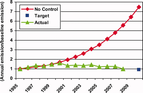
Figure 3. European IC company emission data from 1995 to 2008.
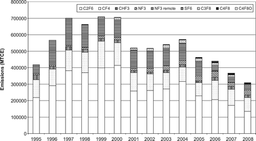
Looking at the data of , it can be appreciated that the 2008 emissions within ESIA are 26% below the 1995 emissions, hence therefore the 2010 target has already been met. However, it should be noted that, due to the current worldwide economic difficulties, overall device production levels have dropped significantly from the fourth quarter of 2008 onwards. Hence, PFC use and emissions are expected to drop likewise. In view of this – presumably temporary – downturn, companies are likely to delay some of the originally planned necessary investments. This makes the final picture rather unclear until such time as the effects of the current downturn have been annulled and the industry has fully recovered.
Collaboration is crucial to the success of the semiconductor industry in meeting the challenging reduction target of 10% in absolute emissions in 2010 versus the baseline year (which after all, means a reduction of about 90% of what the emission would have been if there had been no reduction effort).The cooperative effort by the members of the WSC to reduce PFC emissions is an excellent example of what can be accomplished by a joint approach. Because the PFC emission reduction program is considered to be pre-competitive, members freely share information on techniques and strategies. One of the key success factors has also been the strong involvement of equipment and gas suppliers to the semiconductor industry.
5 Conclusions
The global semiconductor industry, although being a minor contributor to overall emissions and in spite of the high costs associated with emission reduction in the sector, accepts full responsibility for making its contribution to reduce global warming by voluntarily reducing its emissions of PFC gases. As the first industry to coordinate globally and establish a voluntary GHG emissions reduction goal, the semiconductor industry has established itself as a leader and model for other industrial sectors.
The semiconductor industry's 10% reduction goal will be reached in 2010, despite a significant increase in wafer demand over time and despite the current economic difficulties. The latter may have caused some intended investments to be delayed in 2009.
The cooperative effort by the members of the WSC to reduce PFC emissions is an excellent example of what can be accomplished by collaboration. Because the PFC emission reduction program is considered to be pre-competitive, members freely share information on techniques and strategies. One of the key success factors has also been the strong involvement of equipment and gas suppliers to the semiconductor industry.
Beyond 2010, it will be a very significant achievement for the global semiconductor industry to maintain its absolute PFC emissions at the 2010 levels. Continuous production growth, as well as new technological developments, will likely lead to higher PFC consumption, whereas the reasonably affordable PFC emission reduction measures are already in place.
Table 1. Greenhouse gases: GWPs and atmospheric lifetimes.
Acknowledgment
The authors thank Shane Harte from ESIA for supporting them with market data and helpful discussions.
Related Research Data
References
- Allgood , C , Hsu , S , Birmingham , B and Soucy , J . A Critical Comparison of Chamber Cleaning Processes in an Applied Materials PECVD Tools. Proceedings of the SEMICON Southwest `A Partnership for PFC Emissions Reductions' Seminar, paper #9. Austin October 16, 2000 .
- Reduction of perfluorocompound (PFC) emissions . 2005 . 2005 State-of-the-Technology Report Technology Transfer #05104693A-ENG, International SEMATECH
- European Commission Report on Greenhouse gas emission trends and projections in Europe . 2008 . Tracking progress towards Kyoto targets. EEA Report No 5/2008, www.eea. europa.eu/publications
- Forster , P , Ramaswamy , V , Artaxo , P , Berntsen , T , Betts , R , Fahey , D W , Haywood , J , Lean , J , Lowe , D C Myhre , G . 2007 . “ Changes in atmospheric constituents and in radiative forcing ” . In Climate change 2007: the physical science basis. contribution of working group I to the fourth assessment report of the intergovernmental panel on climate change , Edited by: Solomon , S , Qin , D , Manning , M , Chen , Z , Marquis , M , Averyt , K B , Tignor , M and Miller , H L . Cambridge, United Kingdom and New York, NY, , USA : Cambridge University Press .
- Intergovernmental Panel on Climate Change . 2006 . “ IPCC guideline for national greenhouse gas inventories, vol 3 – Edited by Simon Eggelston, Leandro Buendia, Kyoko Miwa, Todd Ngara, Kiyoto Tanabe. Published by the Institute for Global Environmental Strategies (IGES) for the IPCC ISBN 4-88788-032-4 ” .
- Jochen , H , (Ecofys) , Winfried , S and (Öko-Recherche) . 2003 . Costs and the impact on emissions of potential regulatory framework for reducing emissions of hydrofluorocarbons perfluorocarbons and sulphur hexafluoride; [cited 20 January 2010]. Available from: http://www.oekorecherche.de/english/berichte/kurzfassungen/kurzRestrict.html