
ABSTRACT
Conductive fillers made from metal nanoparticles offer many advantages for the fabrication of a variety of electronic devices, but when they have a porous structure, their poor conductivity limits their adoption in many applications. In this study, an Ag-coated Cu micro-nanoparticle paste is used to achieve compact filling of blind vias on flexible copper clad polyimide laminates through a multistep filling and sintering technique. The filled blind vias achieve a resistivity as low as 6.2 μΩ·cm, which is comparable that of electroplated blind vias. Higher sintering pressure and temperature promote the filling performance, while the conductivity deteriorates at a via depth/diameter ratio greater than 1:1. Finite element simulations reveal a stress inhomogeneity in vias with large depth/diameter ratios, which is the key to understanding the evolution of the conductive properties of a paste-filled via. This study provides an effective method for high-performance microvia filling as well as insights into the mechanism that influences its performance.
Graphical abstract
1. Introduction
As electronic devices and integrated circuits continue to be driven toward high integration and miniaturization, advanced packaging technologies, such as 3D packaging and system-in-package, are attracting greater attention. Microvia filling is a fundamental technique for these advanced packaging technologies, as it provides channels for vertical electrical interconnection and signal communication between packaging layers, and thereby improves the communication rate and efficiency and reduces the volume and power consumption of electronic devices. With these advantages, microvia filling technology can be applied broadly in all levels of electronic packaging and manufacturing.
At present, electroplating is the main method used for microvia filling in the electronic industry. To achieve voidless filling of the vias, the deposition rate of copper at the bottom of the vias should be larger than that on the surface, a processing method known as the bottom-up filling mode [Citation1]. By controlling additives (levelers, accelerators, and inhibitors) in the plating solution, the bottom-up filling mode can be achieved. However, the current electroplating microvia filling method also has some drawbacks. First, electroplating is a relatively complex multistep process that includes exposing, developing, etching, and plating procedures, and the byproducts are environmentally unfriendly [Citation2]. Second, for microvias with a large depth/diameter ratio, the concentration of additives and the current density must be controlled precisely. Because of the narrow processing windows that such precise control demands, it is difficult to achieve the bottom-up filling mode, and filling defects such as internal voids, seams, and dimples are prone to occur [Citation3,Citation4]. For microvias with a large depth and diameter, the electroplating filling efficiency will be low [Citation5]. Third, due to the interfacial resistance of the metal seed layer and the influence of electroplating additives, the electrical properties of electroplating-filled vias are significantly lower than that of bulk copper [Citation3,Citation6].
In recent years, a direct microvia filling method that uses conductive fillers made with metallic particle has emerged. Extensive research has been conducted to explore the application of metal particle pastes as die attach materials for electronic packaging [Citation7–9]. For a microvia filling process, the metallic particle conductive fillers are directly printed into the vias and are cured or sintered at temperatures of 150–300°C to achieve electrical interconnection [Citation10,Citation11]. For example, Falat et al. [Citation12] used Ag nanoparticles (Ag NPs) to fill microvias with a depth and diameter of 100 and 30 μm, respectively, on polyimide (PI) substrates, and the filled vias had a resistance of 251.2 mΩ after sintering at 250°C for 30 min, corresponding to a resistivity of 5.6 × 10³ μΩ·cm. Zhou et al. [Citation13] used Ag micro-flakes to fill microvias with a depth and diameter of 1000 and 250 μm, respectively, in isolated printed circuit board layers and obtained a resistivity of 180 μΩ·cm after curing at 150°C for 30 min. Li et al. [Citation14] used Cu/Sn particle-based conductive fillers to fill vias with a depth and diameter of 370 and 100 μm, respectively, on epoxy molding compound boards, and the filled vias had a resistance of 29 mΩ after sintering at 260°C for 30 min, corresponding to a resistivity of 730 μΩ·cm. Compared to the electroplating filling technology, the use of conductive fillers has the advantages of a simpler procedure (avoiding time-consuming steps such as seed layer deposition and masking), a higher filling efficiency for large and deep vias, the ability to fill microvias with different sizes and depth/diameter ratios on different substrates, and eco-friendliness. However, due to the gaps that can form in the metal particle fillers, it is difficult for the fillers to obtain a void-free sintered structure. The resistivity of the microvias filled with metal particles is still 2–4 orders magnitude higher than that of bulk copper, which is unsatisfactory for advanced electronic packaging. Improving the microvia filling performance of metal particles and understanding the factors that affect the structure and electronic properties are crucial for increasing the number of applications of conductive fillers.
In this study, an Ag-coated Cu micro-nanoparticle (Cu@Ag MNP) paste is used to fill blind vias on flexible copper clad PI laminates. The Cu@Ag MNPs have better oxidation resistance than Cu MNPs and have a high weight ratio (~85 wt. %) in the paste. Another component of the paste is ethylene glycol, which is volatile, decomposes easily, and leaves no organic residue after sintering. Through a multistep filling and sintering technique, filled microvias with promising performance are obtained. The effects of sintering pressure and temperature as well as depth/diameter ratio on the filling performance of the vias are systematically explored. Based on the sintering mechanisms of metal MNPs and the stress inhomogeneity in the vias, as revealed by finite element simulations, the evolution of the structure and properties of the filled microvias are presented and explained.
2. Experimental
2.2. Material preparation
Cu MNPs (analytical purity, with a size of ~710 nm), AgNO3 (analytical purity), L-histidine (analytical purity), and ammonia (analytical purity, 25%) were purchased from Aladdin Biochemical Technology Co. Ltd., Shanghai, China. Polyethylene glycol (PEG, analytical grade, molecular weight = 1000 g/mol) was purchased from Solarbio Technology Co., Ltd., Beijing, China. Ethylene glycol (analytical purity) was purchased from Sinopharm Chemical Reagent Co., Ltd., Shanghai, China.
L-histidine and PEG were dissolved in 50 mL of deionized water to achieve concentrations of 0.26 and 0.04 mol/L, respectively. Then 0.64 g of Cu MNPs was added into the solution and dispersed by ultrasonic treatment. After mechanical stirring for 10 min, 0.6 mL of 0.08 mol/L ammonia was added to the solution and stirred for 1 min to remove the residual oxides on the surface of the Cu MNPs. In a separate solution, AgNO3, ammonia, L-histidine, and PEG were dissolved in 200 mL of deionized water to achieve concentrations of 0.005, 0.2, 0.26, and 0.04 mol/L, respectively, and then treated with the same ultrasonic treatment and mechanical stirring for 10 min. Then the solution with Cu MNPs was poured into the second solution and reacted for 20 min with an ultrasonic treatment and mechanical stirring to obtain the Cu@Ag MNPs. The Cu@Ag MNPs were extracted from the solution by centrifugation at 12,000 rpm for 5 min, washed 3 times with deionized water and once with ethanol, and dried in vacuum at room temperature for 8 h. Finally, the Cu@Ag MNPs were mixed with ethylene glycol at a weight ratio of 4:1 with a high-speed mixer (SpeedMixer DACC, Hamm, Germany) at 2000 rpm for 2 min to prepare the Cu@Ag MNP paste as a conductive filler for microvias.
2.2. Microvia filling experiment
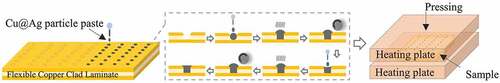
Flexible copper clad laminates (FCCLs) with blind vias were used as the substrate. The thickness of the FCCLs was 70 μm, including 30-μm-thick PI in the center and 20-μm-thick Cu laminates on both surfaces. The diameters of the blind vias were 35, 50, 75, and 100 μm. The microvias were filled with the as-prepared Cu@Ag MNPs with a multistep filling method, as shown in . First, the Cu@Ag MNP filler was printed into the microvias using a nozzle. Then the samples were kept under vacuum for 3 min, during which the air inside the microvias could escape and the pastes permeated into the microvias due to capillary effects. Then the upper surface of the sample was roll pressed to compact the paste into the microvias. More Cu@Ag MNP paste was then applied on the top of the microvias and dried under a 100°C air gas flow for 3 min, during which the ethylene glycol solvent in the paste evaporated. The sample was then roll pressed again to further compact the filling. Finally, the sample was clamped between two glass plates and sintered at 220, 260, or 300°C and 0.5, 1, or 2 MPa in a hot press furnace in a 95:5 Ar–H2 atmosphere. For a typical sintering process, the temperature was ramped up to the pre-curing temperature of 130°C at a heating rate of 6°C/min, held there for 5 min, ramped up to the desired sintering temperature at the same rate, held for 30 min, and then cooled naturally.
Figure 1. Illustration of the microvia filling and sintering procedures.
2.3. Characterization
A scanning electron microscope (SEM, Hitachi SU8220, Tokyo, Japan) and a high-resolution transmission electron microscope (HR-TEM, FIB Talos F200S, Hillsboro, USA) were used to observe the morphologies of the as-synthesized Cu@Ag MNPs and the filled microvias after sintering. The size distribution of the particles was obtained based on statistics of arbitrarily observed 500 particles in the SEM micrographs using the ImageJ software. To observe the cross-section morphology of the filled microvias, the samples were embedded in the epoxy resin and then ground and polished by a polish-grinding machine (DINCER MoPao260E, Laizhou, China), and then milled by an ion beam milling systems (Leica RES102, Heidelberg, Germany). The element distribution of the Cu@Ag MNPs was analyzed with an energy dispersive spectrometer (EDS, Bruker XFlash 6|30, Karlsruhe, Germany). The chemical composition of the Cu@Ag MNPs was measured by an Inductively Coupled Plasma Mass Spectrometry (ICP-MS, Thermo Fisher ICAP RQ). The phase composition of the as-synthesized Cu@Ag MNPs was characterized by an X-ray diffractometer (XRD, Bruker D8 Advance, Karlsruhe, Germany) with a scan rate of 10 °/min over a 2θ range of 20–80°. The thermal decomposition processes of the Cu@Ag MNPs, Cu@Ag MNP paste, ethylene glycol, L-histidine and PEG were detected by a Mettler Toledo thermogravimetric (TG) analyzer in Ar atmosphere from room temperature to 900°C with a heating rate of 10°C·min−1. The resistivity values of the sintered microvias were measured by the four-point probe method using a test platform (Four Probe Technology Co., Ltd., ST-102E, Guangzhou, China) with a source meter unit (Keithley, 6220) and a nanovoltmeter (Keithley, 2182A) [Citation15].
2.4 Microvia sintering stress field simulation
Finite element simulations using the ANSYS program are employed to explore the stress field distribution during the hot-pressing sintering process of the microvias. shows a sketch of the simulation model. The substrate contains a PI layer and upper and lower copper layers, which have the same thickness as in the experiments. A blind via is located at the center of the model, which is filled with the Cu@Ag MNP paste. The diameter of the microvia is set as 35, 50, 75, or 100 μm, matching the experiments. The upper surface of the sample is also covered by the Cu@Ag MNP paste, with a thickness of 20 μm. The model is meshed automatically into tetrahedron elements by the program, as shown in . A ‘SOLID185’ element type is used. A pressure of 2 MPa is applied to the upper surface of the model. The material properties used in the simulations are shown in . The stress field in the model under the loading situation is simulated by the static elastic analysis of the program.
Figure 2. (a) Sketch of the finite element simulation model. (b) Cross-section sketch of the finite element simulation model showing the microvia. (c) Element mesh of the model.
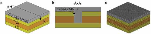
Table 1. Properties of the materials in the simulations.
3. Results
3.1 Characterization of Cu@Ag MNPs
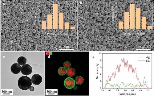
shows the SEM images of the Cu MNPs and the as-prepared Cu@Ag MNPs. The Cu@Ag MNPs are dispersed without obvious aggregation. The Cu MNPs and Cu@Ag MNPs are 300–1300 nm in diameter. The average size of the Cu MNPs and the Cu@Ag MNPs is measured to be 710 and 750 nm, respectively. shows an HR-TEM image of the as-prepared Cu@Ag MNPs and the distribution of Cu and Ag in the Cu@Ag MNPs. A Cu core and Ag shell structure can be observed. The inset in shows the element distribution along the diameter direction of a single Cu@Ag MNP. The signal of Cu forms a peak in the center, and the signal of Ag forms two peaks at the edges, confirming the core-shell structure of the Cu@Ag MNPs. Based on the element mapping, the thickness of the Ag shell is estimated to be 50–100 nm. The ICP-MS result shows that the element ratio of Cu:Ag in the Cu@Ag MNPs is 73.9: 26.1 wt.%. According to this ratio, if the Ag shell is uniformly coated on the Cu core, the Ag shell thickness will be ~5.5% of the particle diameter, which basically agree with the observation of the EDS map.
Figure 3. (a) SEM image of the Cu MNPs. (b) SEM image of the Cu@Ag MNPs. (c) TEM image of the Cu@Ag MNPs. (d) EDS map of Cu@Ag MNPs. (e) Element mapping of the Cu@Ag MNPs.
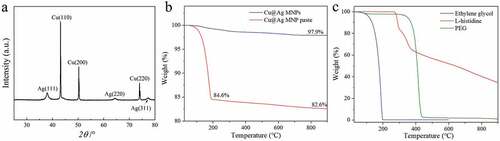
shows the XRD pattern of the as-prepared Cu@Ag MNPs after storage in air for 30 days. Peaks of silver can be observed at the positions of 2θ = 38.1, 64.4, and 77.4°, corresponding to the (111), (220), and (311) crystal planes, respectively. Peaks of copper can be observed at 2θ = 43.2, 50.4, and 74.0°, corresponding to the (111), (200), and (220) crystal planes, respectively. No peaks of copper oxide or silver oxide can be observed in the XRD pattern, indicating the relatively good oxidation resistance of the as-prepared Cu@Ag MNPs. shows the TG curves of the as-prepared Cu@Ag MNPs and Cu@Ag MNP paste. shows the TG curves of ethylene glycol, L-histidine and PEG. It can be found that the weight of the Cu@Ag MNPs decreases in the temperature range from 100 to 700°C and reaches a plateau above 700°C. The weight loss corresponds to the decomposition or evaporation of residual organics. The total weight loss at 900°C is about 2.1%. On the other hand, the weight of the Cu@Ag MNP paste dropped sharply between 100°C and 200°C. It corresponds to the evaporation of the ethylene glycol solvent represented by the blue curve in . Based on the weight fraction at 200°C, a solids content of about 84.6% can be estimated. With the further increase of temperature, the Cu@Ag MNP paste loses weight slowly, and the weight fraction reaches 82.6% at 900°C. The weight loss between 200°C and 900°C is about 2%, which is basically consistent with the TG curve of the Cu@Ag MNPs. From the measured TG curves, it can be inferred that the residual organic content in the Cu@Ag MNPs is about 2%, which may originate from the L-histidine and PEG in the reaction solvent. The role of these two additives is to improve the quality of the Cu@Ag MNPs during the preparation, but they will not promote the sintering process of the particles. As a complexing agent, L-histidine can regulate the deposition potential of Ag ions and thereby improve the coating quality of the Cu@Ag particles [Citation19,Citation20]. PEG is a commonly used dispersant in the preparation of metal nanoparticles, which can prevent the agglomeration of the particles [Citation21].
Figure 4. (a) XRD pattern of the as-prepared Cu@Ag MNPs after storage in air for 30 days. (b) TG curves of the as-prepared Cu@Ag MNPs and Cu@Ag MNP paste. (c) TG curves of ethylene glycol, L-histidine and PEG.
3.2 Effect of sintering pressure on the microvia filling performance
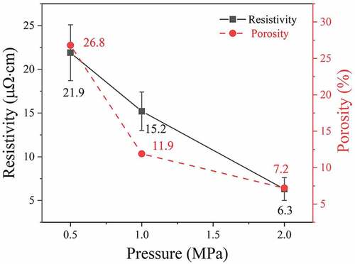
shows cross-section images of filled microvias with a depth and diameter of 50 and 75 μm, respectively, after sintering at 260°C under pressures of 0.5, 1, or 2 MPa for 30 min. The electrical resistivities and porosities of the filled vias are measured and shown in . At a relatively low pressure of 0.5 MPa, the sintered structure still shows the spherical outlines of the original Cu@Ag MNPs, and notable gaps can be observed between the Cu@Ag MNPs. These gaps interconnect with each other and form a network. Based on the cross-section image, the porosity of the sample is estimated to be 26.8%. The electrical resistivity of the sample is measured to be 21.9 μΩ·cm. As the pressure increases to 1 MPa, spherical outlines of the Cu@Ag MNPs can still be observed, but the gaps between the Cu@Ag MNPs become smaller. The porosity of the sample decreases to 11.9%, and the electrical resistivity of the sample decreases to 15.2 μΩ·cm. At a pressure of 2 MPa, the outlines of the original Cu@Ag MNPs are indistinguishable, and the shape of the internal gaps changes from a connected network to small, dispersed pores. This change indicates that the Cu@Ag MNPs have been completely sintered at this pressure and merged with each other. The enlarged images of the three samples show that the sintered Cu@Ag MNPs have merged well with the original copper laminate at the bottom of the vias under the different sintering pressures. The porosity of the sample decreases to only 7.2%, and the electrical resistivity of the sample decreases to 6.3 μΩ·cm.
Figure 5. Low- and high-magnification cross-section SEM images of the filled microvias with depth and diameter of 50 and 75 μm, respectively after sintering at 260°C and 0.5, 1, or 2 MPa for 30 min. The small red or yellow boxes in each image in the top row indicate from where in each sample the high-magnification images in the bottom two rows with the corresponding frame color were obtained.
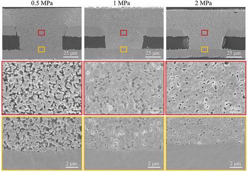
Figure 6. The measured electrical resistivities and porosities of the filled microvias sintered at different pressures.
3.3 Effect of sintering temperature on the microvia filling performance
shows cross-section images of the filled microvias with depth and diameter of 50 and 75 μm, respectively, after sintering at 2 MPa and 220, 260, or 300°C for 10 or 30 min. The measured electrical resistivities and porosities of the filled vias are shown in . At the shorter sintering time of 10 min (), the sample sintered at the relatively low sintering temperature of 220°C still shows the spherical outlines of the original Cu@Ag MNPs, and there is an obvious gap between the sintered Cu@Ag MNP layer and the original copper laminate. This indicates that the Cu@Ag MNPs have not been sufficiently sintered at this low temperature. The porosity of the filled via is 10.8%, and the measured electrical resistivity is 51.0 μΩ·cm. As the sintering temperature increases to 260°C, a compact sintering structure with only small voids is obtained, and there is no gap between the sintered Cu@Ag MNP layer and the original copper laminate. The porosity of the filled via decreases to 8.5%, and the electrical resistivity is reduced to 8.8 μΩ·cm. As the temperature is increased further to 300°C, the morphology and properties of the sintering structure is almost unchanged, with a porosity of 6.0% and an electrical resistivity of 10.6 μΩ·cm. When the sintering time is extended to 30 min, the samples sintered at 220, 260, and 300°C obtain compact sintering structures (), and the measured resistivities and porosities of the samples are 8.2, 6.3, and 8.8 μΩ·cm and 13.1, 7.2, and 5.6%, respectively.
Figure 7. Low- and high-magnification cross-section SEM images of the filled microvias with depth/diameter of 50/75 μm after sintering at 220, 260, or 300°C under a pressure of 2 MPa for (a) 10 min and (b) 30 min. The small red and yellow boxes in each image in the top row indicate from where in each sample the high-magnification images with the corresponding frame color in the bottom two rows were obtained.
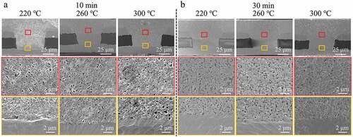
Figure 8. The measured (a) electrical resistivities and (b) porosities of the filled microvias sintered at different temperatures and times.
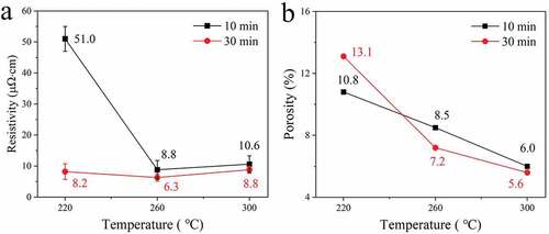
Although it is commonly understood that the resistivity of metal particles decreases with increasing sintering temperature, the results of this study suggest that increasing the temperature further beyond 260°C does not significantly improve performance of Cu@Ag particles and may even result in higher resistance. Some previous studies have also found that the resistivity of sintered Cu@Ag particles will increase slightly when the temperature exceeds 260°C [Citation22]. Such an abnormal increase of resistivity is probably a result of the dewetting phenomenon of Ag shells, which has been widely noticed in the previous studies of Cu@Ag particles [Citation23–26]. Due to the lattice mismatch of 11.7% between Cu and Ag, the Cu-Ag interface is instable [Citation27]. Under a relatively high heating temperature, the Ag shell tends to form Ag nodules, and the inner copper core would be exposed and might react with the residual oxygen in the atmosphere to form copper oxide, resulting in the increased resistivity [Citation26].
3.4 Effect of depth/diameter ratio on the microvia filling performance
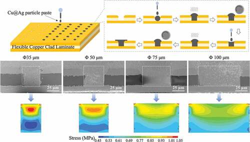
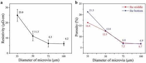
shows cross-section images of the filled microvias with diameters of 35, 50, 75, and 100 μm and a depth of 50 μm after sintering at 260°C and 2 MPa for 30 min. The electrical resistivities and porosities of the filled vias are measured and shown in . For the sample with a diameter of 35 μm, the outline of the original Cu@Ag MNPs can still be observed after sintering, and there is an obvious gap between the Cu@Ag MNP layer and the original FCCL. The porosity in the middle of the via is about 16.4%, and this value increases to 21.3% near the bottom of the via. This morphology indicates that the Cu@Ag MNPs have not been sufficiently sintered in the via that has a relatively high depth/diameter ratio. The average measured electrical resistivity of the filled vias is 25.0 μΩ•cm. For the samples with diameters of 50, 75, and 100 μm, more compact sintering structures with small voids are obtained. The metallurgical bonding between the Cu@Ag MNP layer and the copper laminate is also significantly improved. The measured porosities and electrical resistivities of the samples with diameters of 50, 75, and 100 μm are 12.5, 7.2, and 6.7% and 11.3, 6.3, and 6.2 μΩ·cm, respectively. These results indicate that the filling performance depends strongly on the depth/diameter ratio of the samples. With a depth/diameter below 2:3 (the samples with diameters of 75 and 100 μm), promising filling performance can be obtained, with relatively small porosity and resistivity. However, if the depth/diameter increases further, the filling performance deteriorates, with notably increased porosity and resistivity.
Figure 9. Low- and high-magnification cross-section SEM images of the filled 50-μm-deep microvias with diameters shown on the top row, sintered at 260°C and 2 MPa for 30 min. The red, yellow, and green boxes in each image in the top row indicate from where in each sample the high-magnification images with the corresponding frame color in the bottom three rows were obtained.
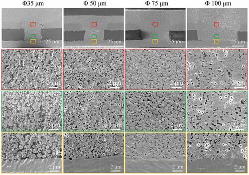
Figure 10. Measured (a) resistivity and (b) cross-section porosity of the filled microvias with different diameters after sintering at 260 °C and 2 MPa for 30 min.
4. Discussion
In , we directly compare our results with previous reports of microvia filling performance of metal-based conductive fillers, demonstrating the promising filling performance of Cu@Ag MNPs in this study. For example, for blind vias with the same depth/diameter ratio of 1:1, Cho et al. [Citation28] filled vias with a diameter of 100 μm by inkjet printing and sintering of Ag NPs, and the filled vias had a resistance of 0.1 Ω, corresponding to a resistivity of 785 μΩ·cm. In this study, we fill vias with a smaller diameter (35–100 μm) by printing and sintering Cu@Ag MNPs, and obtain a resistivity of only 6–25 μΩ·cm, which is much lower than the previously reported values. For the samples with a diameter of 100 μm after sintering at 260°C and 2 MPa for 30 min, the lowest resistivity of 6.2 μΩ·cm is reached, corresponding to a conductivity of 1.6 × 10⁷ S/m. Such performance is comparable to that of electroplated microvias, with a typical conductivity of 1.67 × 10⁷ S/m [Citation29].
Figure 11. Comparison of microvia filling performance of metal-based conductive fillers in references [Citation13,Citation30–32] and in this study.
![Figure 11. Comparison of microvia filling performance of metal-based conductive fillers in references [Citation13,Citation30–32] and in this study.](/cms/asset/827a4b31-9af8-4687-8f00-4e20382ae7e4/tsnm_a_2107114_f0011_c.jpg)
The superior microvia filling performance of this study can be understood from two aspects:
(1) Materials design
Cu and Ag particles have been used to fill microvias in previous reports [Citation31]. However, Cu particles are easily oxidized in air [Citation30,Citation32], and Ag particles are prone to electromigration [Citation33], which limit the use of these two kinds of particles. To prepare the conductive filler, some studies mixed the metal particles with a non-conductive polymer matrix such as epoxy resin and phenolic resin. The polymers play the role of adhesive and can keep the particles in contact with each other to achieve electric conduction after curing at the relatively low temperature of ~180°C [Citation34,Citation35]. However, such a temperature is not sufficient for the metal particles to form thick sintering necks with each other. The epoxy resin and phenolic resin, with a vaporization temperature of 300 ~ 500°C [Citation36], are nonvolatile under the curing temperature. As the metal particles are only in physical contact and lack metallurgical bonds, there is still a large contact resistance between the particles, resulting in poor overall conductivity. Another group of studies has prepared conductive inks and pastes by mixing the metal particles with an organic flux such as rosin, alcohol, or oleic acid, which have a relatively low vaporization temperature of 180 ~ 250°C [Citation37,Citation38]. The solid content in these composites is 40–85 wt. %. With less solid content, the conductive ink has lower viscosity (0.001–0.1 Pa·s [Citation39]) and can more easily fill the vias with small diameter and large depth. To achieve metallurgical bonding, these metal particle inks/pastes need to be sintered at a relatively high temperature, greater than 220°C [Citation40]. After comparing the conductivities of metal-based conductive fillers in literatures, it can be found that the conductivity of fillers containing volatile organic additives is about 1–2 orders of magnitude higher than that of fillers containing nonvolatile organic additives [Citation10].
In this study, we mixed the Cu@Ag MNPs with ethylene glycol as the filling material. The ethylene glycol is volatile at a temperature near 200°C [Citation37,Citation38,Citation41], which is confirmed by the TG curve in . The content of residual organics is in the particles are relatively small, as revealed by the TG curve in . The solid content of the paste is relatively high (~85 wt.%), which is beneficial in terms of more readily achieving greater compactness [Citation42]. The sizes of the Cu@Ag MNPs range widely from 300 to 1300 nm. It has been revealed that a broad size distribution may promote dense packing of the particle fillers, as small particles can fill the gaps between large particles [Citation43]. For these reasons, it can be expected that the Cu@Ag MNPs could achieve better filling performance.
(2) Filling method
Filling density is a key factor for the microvia filling performance of metal particles. The traditional screen-printing method provides an easy way to fill vias and grooves. However, as the depth/diameter ratio of the vias increases, it becomes more difficult for the particles to fill the bottom of the vias, and external pressure is needed to promote the filling process, such as in the extrusion printing method. There is a contradiction between the ability of the particle paste to fill a via and to achieve a high density after sintering. The viscosity of the particle paste with lower solid content and larger particle diameter is lower, and the paste can more easily fill the vias. However, the sintering property of the paste is poor, as the gaps between particles leave pores in the sintered structure. In this study, a multistep filling method is used to improve the ability of the particle paste to fill the vias, with less influence on the sintering properties. First, the wet particle paste is printed into the vias with the assistance of external pressure. Then the paste is dried and the solution in the paste evaporates. After that, the paste is pressed again to further compress and eliminate any voids. By this process, a better filling density can be achieved.
Using the Cu@Ag MNPs and the multistep filling method, promising filling performance is achieved. It is also found that the filling performance of the Cu@Ag MNPs improves with increasing sintering temperature and pressure. Such a trend has been broadly observed in studies of die-attach bonding and the sintering performance of metal particles [Citation38]. The sintering of metal particles is a kinetic process related to the growth of sintering necks [Citation44]. With increasing temperature, this kinetic process is accelerated so that better sintering properties can be obtained [Citation45]. When the sintering temperature is sufficiently high, large sintering necks form between the particles, and there is little performance improvement provided by further temperature increases [Citation22,Citation30]. During the sintering process, the external pressure can also promote the closure of internal voids in the sintering structure. Therefore, better sintering performance can be obtained under a higher sintering pressure [Citation46]. According to the results in , 220 and 260°C are the proper temperatures for sintering the Cu@Ag MNP paste at a pressure of 2 MPa and sintering times of 10 or 30 min.
In , it is noticeable that the depth/diameter ratio has a significant influence on the microvia filling performance, especially for microvias with a depth/diameter above 1:1. One possible reason is that due to the viscosity of the metal particle paste (about 5 and 30 Pa·s [Citation47,Citation48]), it becomes difficult for the particle paste to fill a narrow microvia. Therefore, the filling density of the metal paste will decrease with decreasing microvia diameter. It is consistent with the measured porosity from the cross-section of the samples. Besides, the stress in the microvia under pressure could be non-uniform, due to the different modulus of the materials. To understand this effect, finite element simulations are utilized to explore the stress field during the sintering process in the filled microvias with different depth/diameter ratios. The simulated compressive stress fields are shown in .
Figure 12. Simulated compressive stress distribution of microvias with a depth of 50 μm and diameters shown on the top row. The bottom row of images shows the stress distribution within the via, which is outlined in the image above by a dashed rectangle.
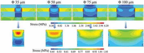
The simulations show that the stress distribution within the sample is not uniform. The stress inside the microvia is relatively low, and the stress outside the microvia is relatively high. The reason for this nonuniform stress is that the modulus of each part of the sample is different, such that the stiffer locations experience higher stress. In the simulations, the modulus of the metal particle paste is set to 10 GPa, which is much lower than that of bulk metal (~100 GPa [Citation18]) and also lower than that of sintered metal particles (on the order of 10 GPa [Citation49]). This is because the metal paste has many pores before sintering, and no sintering neck is formed, such that it is still prone to deformation. Chen et al. [Citation50] have determined that the modulus of Ag NP paste is 6–10 GPa. Because the modulus of the metal particle paste is lower than that of the substrate, the stress inside the microvia will be lower than outside the microvia.
From the enlarged stress field distribution (), it is also found that the stress inside the microvia is not uniform, and a low stress area is formed near the bottom of the microvia. The stress inhomogeneity becomes more pronounced in the microvias with a higher depth/diameter ratio. The porosities in the middle and bottom of the sintered microvias are remeasured and shown by the red and blue curves in , respectively. For the samples with a diameter above 50 μm, the measured porosities in the middle and bottom of the microvias are almost equal. For the samples with a diameter 35 μm, the porosity at the bottom of the microvia is obviously higher. The low stress at the the bottom of the microvia revealed by the simulations could reasonably explain the uneven distribution of porosity in the microvias with small diameter.
5. Conclusion
A facile microvia filling method of printing and sintering Cu@Ag MNPs is proposed. Cu@Ag MNPs with good sphericity and promising oxidation resistance are prepared through a liquid chemical replacement reaction method and are mixed with ethylene glycol into a paste with a solid content of ~85 wt. % to create the conductive filler. The paste is filled and compacted into blind vias on flexible FCCL substrates through a multistep filling procedure and are sintered by heat and pressure. It is shown that higher sintering pressure and temperature can promote the sintering process of the Cu@Ag MNPs, and thereby improve the properties of the filled microvias. After sintering at 260°C and 2 MPa for 30 min, a 100 μm diameter microvia can obtain a porosity as low as 6.7%, and a resistivity as low as 6.2 μΩ·cm. Such performance is comparable to that of electroplated blind vias. With these advantages, this method has broad application opportunities in advanced 3D electronic packaging. It is also found that the conductivity starts to deteriorate at a depth/diameter ratio greater than 1:1. Through finite element simulations, we can see that the stress field in the microvia during hot-press sintering is not uniform. Due to the high flexibility of the Cu@Ag MNP paste, the stress in the microvia is lower than that outside the microvia, and a low stress region will form near the bottom of the microvia. This effect becomes more pronounced in the microvias with a large depth/diameter ratio, leading to a deterioration in filling performance. The control and elimination of this effect by changes in the material, microvia shape, and filling process could enable further applications of this method with smaller and deeper microvias.
Acknowledgments
We acknowledge the supports of the National Key R&D Program of China (2018YFE0204601), the Key-area Research and Development Program of Guangdong Province (2021B0101290001, 2020B0101290001), National Natural Science Foundation of China (61874155, 62174039), Guangdong Basic and Applied Basic Research (2021A1515110656, 2022A1515010141, 2021A1515011642), and Open Project of the State Key Laboratory of Advanced Materials and Electronic Components (FHR-JS-202011005).
Disclosure statement
No potential conflict of interest was reported by the author(s).
Data availability statement
The datasets generated during and/or analyzed during the current study are available from the corresponding author on reasonable request.
Additional information
Funding
References
- Moffat TP, Wheeler D, Kim SK, et al. Curvature enhanced adsorbate coverage model for electrodeposition. J Electrochem Soc. 2006;153(2):C127–C132.
- Zhao F. Improvement on fully filled through silicon vias by optimized sputtering and electroplating conditions. Materials. 2019;12(22):3713–3723.
- Zhang Y, Ding G, Wang H, et al. Optimization of innovative approaches to the shortening of filling times in 3D integrated through-silicon vias (TSVs. J Micromech Microeng. 2015;25(4):045009–045021.
- Tao P, Chen Y, Cai W, et al. Effect of copper sulfate and sulfuric acid on blind hole filling of HDI circuit boards by electroplating. Materials. 2020;14(1):85–96.
- Wang F, Ren X, Zeng P, et al. Dynamics of filling process of through silicon via under the ultrasonic agitation on the electroplating solution. Microelectron Eng. 2017;180:25–29.
- Lee S, Chen K. Development of bumpless stacking with bottom–up TSV Fabrication. IEEE Trans Electron Devices. 2017;64(4):1660–1665.
- Wang Q, Zhang S, Lin T, et al. Highly mechanical and high-temperature properties of Cu-Cu joints using citrate-coated nanosized Ag paste in air. Prog Nat Sci Mater Int. 2021;31(1):129–140.
- Zhang S, Wang Q, Lin T, et al. Cu-Cu joining using citrate coated ultra-small nano-silver pastes. J Manuf Processes. 2021;62:546–554.
- Zhang S, Qi X, Yang M, et al. A study on the resistivity and mechanical properties of modified nano-Ag coated Cu particles in electrically conductive adhesives. Journal of Materials Science: Materials in Electronics. 2019;30(10):9171–9183.
- Yang G, Luo S, Li Z, et al. A mini review on the microvia filling technology based on printed metal nano/microparticles. Front Mater. 2022;9:860710.
- Bach HL, Yu Z, and Letz S, et al., Vias in DBC substrates for embedded power modules, CIPS 2018; 10th International Conference on Integrated Power Electronics Systems Stuttgart, Germany, 2018 (), pp. 1–5.
- Falat T, Felba J, and Moscicki A, et al., Nano-silver inkjet printed interconnections through the microvias for flexible electronics, 2011 11th IEEE International Conference on Nanotechnology Portland, OR, USA, 2011, pp. 473–477.
- Zhou G, Mao Y, Wang C, et al. Fabrication of silver electrically conductive adhesive to apply in through-hole filling for PCB interconnection. J Mater Sci-Mater El. 2016;27(9):9186–9190.
- Li X, Ogawa T, and Shibata T, et al., Imprint-through mold via (i-TMV) with high aspect ratio and narrow pitch for antenna in package. 2020 IEEE 70th Electronic Components and Technology Conference (ECTC) Orlando, FL, USA, 2020, pp. 120–125.
- Li J, Zhou G, Wang J, et al. Nickel-nanoparticles-assisted direct copper-electroplating on polythiophene conductive polymers for PCB dielectric holes. J Taiwan Inst Chem Eng. 2019;100:262–268.
- Tan KS, Cheong KY. Mechanical properties of sintered Ag–Cu die-attach nanopaste for application on SiC device. Mater Des. 2014;64(9):166–176.
- Zhang Q-H, Dai M, Ding M-X, et al. Mechanical properties of BPDA–ODA polyimide fibers. Eur Polym J. 2004;40(11):2487–2493.
- Clayton CR. Materials science and engineering: an introduction: by W. D., Callister Jr.; published by Wiley, Chichester, West Sussex, 1985; 602 pp.; price, £40.40. Mater Sci Eng. 1987;94:266–267.
- Yang G, Wang P, Liu Y, et al. Effect of Ag coating on the oxidation resistance, sintering properties, and migration resistance of Cu particles. J Alloys Compd. 2022;923:166271.
- Wu YN, Zhou MM, Zhang BR, et al. Amino acid assisted templating synthesis of hierarchical zeolitic imidazolate framework-8 for efficient arsenate removal. Nanoscale. 2014;6(2):1105–1112.
- Bhogaraju SK, Elger G, Conti F, et al. Die-attach bonding for high temperature applications using thermal decomposition of copper(II) formate with polyethylene glycol. Scripta Mater. 2020;182:74–80.
- Peng YH, Yang CH, Chen KT, et al. Study on synthesis of ultrafine Cu-Ag core-shell powders with high electrical conductivity. Appl Surf Sci. 2012;263:38–44.
- Lee CH, Choi EB, Lee J-H. Characterization of novel high-speed die attachment method at 225 °C using submicrometer Ag-coated Cu particles. Scripta Mater. 2018;150:7–12.
- Choi EB, Lee JH. Dewetting behavior of Ag in Ag-coated Cu particle with thick Ag shell. Appl Surf Sci. 2019;480(JUN.30):839–845.
- Kim MI, Lee JH. Die sinter bonding in air using Cu@Ag particulate preform and rapid formation of near-full density bondline. J Mater Res Technol. 2021;14:1724–1738.
- Hai HT, Takamura H, Koike J. Oxidation behavior of Cu–Ag core–shell particles for solar cell applications. J Alloys Compd. 2013;564:71–77.
- Bochicchio D, Ferrando R. Morphological instability of core-shell metallic nanoparticles. Phys Rev B. 2013;87(16):165435.
- Cho C-L, Kao H-L, Chang L-C, et al. Inkjet-printed vertical interconnects for ultrathin system-on-package technology. Surf Coat Technol. 2019;359:85–89.
- Li Z, Tan B, Shi M, et al. Bis-(sodium sulfoethyl)-disulfide: a promising accelerator for super-conformal copper electrodeposition with wide operating concentration ranges. J Electrochem Soc. 2020;167(4):042508.
- Das RN, Egitto FD, Markovich VR. Nano- and micro-filled conducting adhesives for z‐axis interconnections: new direction for high‐speed, high‐density, organic microelectronics packaging. Circuit World. 2008;34(1):3–12.
- Quack N, Sadie J, and Subramanian V, et al., Through Silicon Vias and thermocompression bonding using inkjet-printed gold nanoparticles for heterogeneous MEMS integration, 2013 Transducers & Eurosensors XXVII: The 17th International Conference on Solid-State Sensors, Actuators and Microsystems (TRANSDUCERS & EUROSENSORS XXVII) Barcelona, Spain, 2013, pp. 834–837.
- Yang TH, Guo ZL, and Fu YM, et al., A low temperature inkjet printing and filling process for low resistive silver TSV fabrication in a SU-8 substrate, 2017 IEEE 30th International Conference on Micro Electro Mechanical Systems (MEMS) Las Vegas, NV, USA, 2017, pp. 749–752.
- Das RN, Egitto FD, and Lauffer JM, et al., Influence of carbon, metal-coated polymer, and nano powders on sintering and electrical performance of nano-micro-filled conducting adhesives for z-axis interconnections, 2009 59th Electronic Components and Technology Conference San Diego, CA, USA, 2009, pp. 180–187.
- Wu HP, Liu JF, Wu XJ, et al. High conductivity of isotropic conductive adhesives filled with silver nanowires. Int J Adhes Adhes. 2006;26(8):617–621.
- Zhang R, Lin W, Lawrence K, et al. Highly reliable, low cost, isotropically conductive adhesives filled with Ag-coated Cu flakes for electronic packaging applications. Int J Adhes Adhes. 2010;30(6):403–407.
- Tian Y, Ke M, Wang X, et al. A resveratrol-based epoxy resin with ultrahigh Tg and good processability. Eur Polym J. 2021;147:110282.
- Yang G, Lai H, Lin W, et al. Approaching the structure-property relationship of sintered metal nano/microparticles from the perspective of the agglomerate size effect. Powder Technol. 2022;399:117254.
- Liu X, Wang C, Liu W, et al. Low temperature nanojoining of silver–copper nanopaste as die attach material for high temperature packaging. J Mater Sci-Mater El. 2017;28(7):5446–5451.
- Cano-Raya C, Denchev ZZ, Cruz SF, et al. Chemistry of solid metal-based inks and pastes for printed electronics – a review. Appl Mater Today. 2019;15:416–430.
- Zhang Z, Chen C, Suetake A, et al. Pressureless and low-temperature sinter-joining on bare Si, SiC and GaN by a Ag flake paste. Scripta Mater. 2021;198:113833.
- Zhang Y, Liu Q, Liu Y, et al. Green synthesis of novel in-situ micro/submicron-Cu paste for semiconductor interconnection. Nanotechnology. 2022;33(28):285705.
- Yang G, Lai H, Lin W, et al. A quantitative model to understand the microflow-controlled sintering mechanism of metal particles at nanometer to micron scale. Nanotechnology. 2021;32(50):505721.
- Uche OU, Stillinger FH, Torquato S. Concerning maximal packing arrangements of binary disk mixtures. Phys A Stat Mech Appli. 2004;342(3):428–446.
- Ishizaki T, Watanabe R. A new one-pot method for the synthesis of Cu nanoparticles for low temperature bonding. J Mater Chem. 2012;22(48):25198–25206.
- Liu JD, Chen HT, Ji HJ, et al. Highly conductive Cu-Cu joint formation by low-temperature sintering of formic acid-treated Cu nanoparticles. ACS Appl Mater Interfaces. 2016;8(48):33289–33298.
- Liu Y, Zhang H, Wang L, et al. Effect of sintering pressure on the porosity and the shear strength of the pressure-assisted silver sintering bonding. IEEE Trans Device Mater Reliab. 2018;18(2):240–246.
- Al-Ma’aiteh TI, Krammer O. Non-Newtonian numerical modelling of solder paste viscosity measurement. Soldering Surf Mount Technol. 2019;31(3):176–180.
- Xu C, Willenbacher N. How rheological properties affect fine-line screen printing of pastes: a combined rheological and high-speed video imaging study. J Coat Technol Res. 2018;15(6):1401–1412.
- Kahler J, Heuck N, Wagner A, et al. Sintering of copper particles for die attach. IEEE T Comp Pack Man. 2012;2(10):1587–1591.
- Chen X, Li R, Qi K, et al. Tensile behaviors and ratcheting effects of partially sintered chip-attachment films of a nanoscale silver paste. J Electron Mater. 2008;37(10):1574–1580.