
 ?Mathematical formulae have been encoded as MathML and are displayed in this HTML version using MathJax in order to improve their display. Uncheck the box to turn MathJax off. This feature requires Javascript. Click on a formula to zoom.
Abstract
Conventional methods of thermoplastic manufacture suffer from high capital costs, while fused deposition modeling (FDM) faces the challenge of poor adhesion between printed layers. We have previously shown that carbon nanotubes can be used as electric field susceptors to locally heat the interfaces between printed layers. We also showed that dielectric barrier discharge (DBD) plasma applicators mounted on FDM nozzles can pass current to printed parts for welding. Little is known, however, about the interaction between the electric field and the printed part. In this work, we simulate the internal heating behavior of printed parts with local variations in conductivity. These studies show that thermal penetration scales with conductive surface layer thickness; the results also indicate that conductive inclusions within parts can create hotspots. These findings explain the heating behavior of FDM printed parts when coupled to a DBD applicator and show that inclusions within the parts could create mechanical defects.
Graphical Abstract
1. Introduction
Conventional processing of thermoplastics into desired shapes is accomplished by mature technologies like injection molding. Thermoplastics are a class of polymers that can be easily processed by heating the polymer to soften and cooling the polymer to reharden [Citation1, Citation2]. Generally, thermoplastics are low cost and light weight while also having desirable mechanical strength and solvent or chemical resistance. Thermoplastics such as polycarbonate (PC), polyethylene (PE), and polypropylene (PP) are used in a wide range of applications in the medical, aerospace, automotive, and other fields [Citation3, Citation4]. A downside to injection molding is the large capital cost, which makes custom parts prohibitive [Citation5].
Fused deposition modeling (FDM) is an additive manufacturing technique where thermoplastic materials are melted and deposited along digitally defined paths; additive manufacturing allows the user to quickly design and manufacture customized parts [Citation6]. On the commercial scale, the use of additive manufacturing can greatly avoid capital costs associated with creating specialized manufacturing equipment for multiple unique geometries [Citation5].
However, a common difficulty with using FDM printing is poor adhesion between printed layers [Citation4, Citation7, Citation8]. Most FDM prints are manufactured one layer at a time and subsequently have poor interlayer adhesion because the filament cools before the next layer is extruded and bonds with the existing structure [Citation9, Citation10]. The lack of inter-layer bonding causes bulk tensile strength of FDM parts to be significantly lower than those of injection molded parts [Citation11–13].
Our group has previously explored methods to solve this problem by heating FDM printed parts to improve interlayer adhesion. Specifically, we showed that carbon nanotubes (CNTs) and other susceptors can be used as local heaters at the filament interface; these nanofillers show a rapid heating response to applied electric fields [Citation14–17]. One way to apply such fields is via a dielectric barrier discharge (DBD) plasma applicator mounted on the FDM print nozzle. As printing proceeds, the DBD acts as a non-contact means to pass electric current and induce in-situ heating and welding between printed traces [Citation18–20]. Sweeney et al. used an annular, dielectric-coated electrode with a 3D printer nozzle in the center [Citation21]. During printing, a low frequency electromagnetic field was applied to the disk applicator; the electromagnetic field application enables DBD plasma to form between the applicator disk and the part, which causes local heating at the layer interfaces without a direct electrical contact [Citation22–24]. The high voltage is required to generate this plasma in the gap above the printed part. The printer nozzle serves as the ground for the circuit to be completed. The resulting mechanical properties for nylon were competitive with conventional injection molding.
However, there have been no in-depth investigations of the heating interaction between the electric field and the printed thermoplastic part (with conductive CNT-coated interfaces). Maintaining control over the temperature distribution is critical because polymer reptation across the interface is a function of the local time and temperature. Controlling this temperature during a complex print will have a direct impact on the mechanical reliability of the printed part.
In the current work, the DBD interaction with the printed part was simulated using a coupled finite element method (FEM) to model how printed structures heat (with local variations in conductivity). Two studies were done to capture the in-situ temperature profiles of printed structures with such conductivity variations. The first study models a conductive layer at the surface of the structure nearest to the applicator disk; the thickness of this layer was varied to approximate how localized changes in conductivity can affect heating rate. The second study models a non-uniform dispersion of CNTs within the printed structure which could result in localized heating variations at these points; to simulate these CNT inclusions, high-conductivity spheres were included within the structure at varying distances from the applicator disk.
2. Methods
2.1. Simulations
The simulation was carried out in COMSOL Multiphysics 5.2 (FEM) by coupling the AC/DC Module and the Heat Transfer Module. The simulation solved the Electric fields in frequency-domain for a single frequency of 37 kHz ignoring the additional small noise and frequency deviations in real plasma. Next the heat transfer problem was solved in time-domain using the induced currents inside the solids as a constant volumetric heat source given by
(1)
(1)
where
is the power density in W m−3,
is the bulk conductivity in S/m,
is the electric field intensity in V m−1. The plasma conduction via air was replaced by a time-harmonic voltage source specified on the top boundary of the 3D printed wall. This assumption is valid since the high voltage (above air breakdown voltage) causes the air gap to be extremely conductive allowing the plasma to tunnel via air [Citation25].
The shape of this source resembles the shapes and dimensions of both the applicator disk and the nozzle. The nozzle was approximated by a voltage of 23 kV, which includes the averaged effect of pulse width modulation, and the applicator disk was set at reference potential 0 V. The bulk conductivity of the 3D printed wall can be varied; for example, the top layer can exhibit higher conductivity than the remaining solid part. Another example is when treating defects within the 3D printed wall, they can exhibit higher conductivity.
The outer boundary of the simulation environment was set to 60 °C. All outside thermal boundaries in the sample are exposed to ambient air and lose heat via conduction to the air around it. The power was supplied via the print nozzle and the ground was the applicator disk and the simulation was allowed to run for 100 s. The simulation results remained unchanged when the power was supplied via the applicator disk and the nozzle was grounded. The geometric parameters and the material properties used are provided in Table S1 [Citation26, Citation27].
2.2. Experimental
High-temperature Nylon (HTN) thermoplastic filaments were obtained from Essentium, Inc., with varying nanofiller content (precise nanofiller and loadings are proprietary). Representative values of conductivity were measured using a four-point probe: The probe was used to measure sheet resistance in Ohm/sq. (Ω/□) of films, and in-plane conductivity in Siemens (S) was calculated as a reciprocal of sheet resistance. These values were used as reference points in the simulations.
3. Results
3.1. Conductive layers at the surface
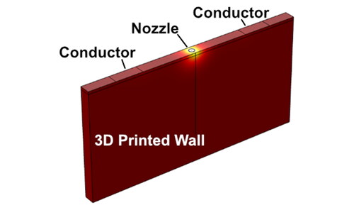
The schematic of the DBD setup in illustrates the 3D printer and printed wall; a DBD applicator disk connected to a power source surrounds a 3D printer head which has extruded a high aspect ratio thermoplastic (nylon) wall. The plasma is generated between the applicator disk and couples with the CNT-filled nylon wall that was extruded. shows a real image of experimental work reported in Sweeney et al.[Citation21] The full simulation geometry can be seen in Figure S1.
Figure 1. a) Schematic of DBD experimental setup; b) image of DBD experimental applicator with a diameter of 5.4 cm; c) COMSOL simulation of 3D printed wall with a single CNT-loaded conductive layer 1 mm in thickness which is coupled to plasma. The wall has a height of 40 mm, length of 80 mm, and width of 4 mm [Citation21].
![Figure 1. a) Schematic of DBD experimental setup; b) image of DBD experimental applicator with a diameter of 5.4 cm; c) COMSOL simulation of 3D printed wall with a single CNT-loaded conductive layer 1 mm in thickness which is coupled to plasma. The wall has a height of 40 mm, length of 80 mm, and width of 4 mm [Citation21].](/cms/asset/5ca5f29a-3b14-4466-ac94-fd7a330cb302/ynan_a_2229187_f0001_c.jpg)
In both the experimental work and simulation work, the print nozzle acts as the ground. An example simulation that reflects this distinction is shown in . In addition, in the simulation, we assumed that only the topmost layer in the z direction of the printed structure is electrically conductive. The finite element simulation first solves the electromagnetic equations to determine the electric field distribution throughout the part. The simulation then computes the time-dependent thermal response to the spatially varying electric field.
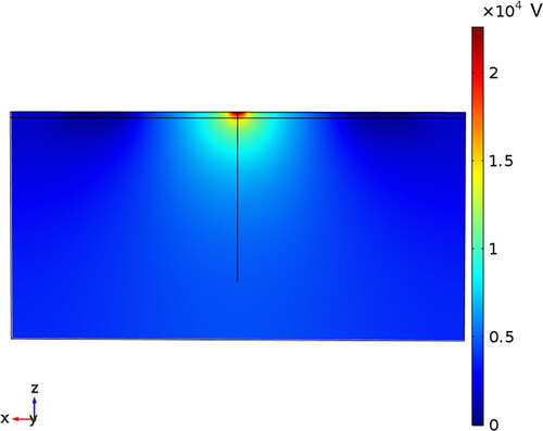
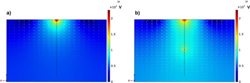
We first examine the electric field that forms when the DBD is coupled with the extruded wall. shows a surface plot of the electric potential (V) through the central X-Z plane of the printed wall. For our model problem, only the top 1 mm of the wall is assumed to be electrically conductive, with an electrical conductivity of 5 × 10⁻⁷ S/m; this mimics the CNT-loaded composite coating in the prior experimental study [Citation21, Citation28]. The electric potential is strongest at the contact point of the nozzle and the weakest at the top surface where power is applied by the applicator disk. The electric field norm is also strongest at the nozzle contact point (Figure S2). The electric field density is greatest below the nozzle, and the electric field streamlines through the wall can be seen in Figure S3.
Figure 2. Electric potential (V) in the center plane of the wall with a conductive surface layer of 1 mm in depth with a conductivity of 5 × 10⁻⁷ S/m. The wall has a height of 40 mm, length of 80 mm, and width of 4 mm.
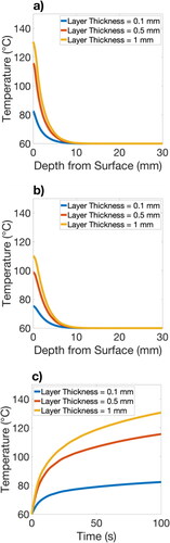
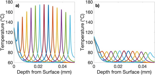
Next, we examine the resulting temperature changes in key locations in the printed wall. show temperature as a function of depth from the top surface of the wall directly below the printer nozzle. shows the temperature profile inside the wall after 100 s of heating. Conductive layer thicknesses of 0.1, 0.5, and 1 mm were analyzed; all three of the simulations show non-uniform heating from 0 to 10 mm and approximately uniform heating below 10 mm. shows the temperature profile directly outside of the wall after 100 s of heating. Similar to the results shown in , there is a significant thermal gradient from 0 to 10 mm. As expected, the max temperature is greater inside the wall than outside the wall. Additionally, the thermal gradient inside the wall is greater than the thermal gradient outside the wall. Similar to our previously published experimental work shown in Figure S5, also shows a decaying temperature profile moving away from the nozzle along the z-axis [Citation21]. shows the transient temperature of the top surface of the wall directly below the printer nozzle for the first 100 s of heating; again, the conductive layer thickness is shown to have a significant effect on the observed heating rate. As this layer becomes thicker, the total generated heat increases.
Figure 3. a) Temperature of the inside of the wall as a function of depth from the top surface, directly below the center of the nozzle at 100 s; b) Temperature of the outside surface of the wall along the z-axis (at the x- and y-center point) at 100 s; c) Temperature of the top surface of the wall directly below the nozzle as a function of time.
3.2. Effects of conductive inclusions
Next, we looked at the case where a conductive inclusion is present in the extruded wall. shows a surface plot of the temperature of a wall with a conductivity of 5 × 10⁻⁷
Figure 4. a) Example of a wall with an inclusion with a conductivity of 1x10⁻⁵ S/m in the center of the wall, directly below the nozzle; b) Center cutaway of a wall with an inclusion with a conductivity of 1 × 10⁻⁵ S/m in the precise center of the wall.
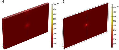
S/m and an inclusion with a conductivity of 1 × 10⁻⁵ S/m directly below the printer head at a depth of 24 mm; shows a cutaway of the central X-Z plane of .
We also looked at the changes to the electric field when a conductive inclusion is present in the extruded wall. shows a surface plot of the electric potential of a wall with a conductivity of 5 × 10⁻⁷ S/m with an inclusion with a conductivity of 1 × 10⁻⁵ S/m at a depth of 1 mm below the top surface of the wall. The directions of the electric field lines are indicated by white arrows. shows a surface plot of the electric potential of a wall with a conductivity of 5 × 10⁻⁷ S/m with an inclusion with a conductivity of 1 × 10⁻⁵ S/m at a depth of 24 mm below the top surface of the wall.
Figure 5. a) Electric potential (V) at the center plane of the wall with an inclusion at a depth of 1 mm. b) Electric potential (V) at center plane of the wall with an inclusion at a depth of 24 mm.
Lastly, we looked at the temperature changes at key locations in the wall when the conductive inclusion is present. shows the temperature profile of the wall with a conductivity of 5 × 10⁻⁷ S/m directly below the printer nozzle where the position an inclusion of 1 × 10⁻⁷ S/m is varied between the top surface of the wall to the bottom of the wall (50 mm) after 100 s of heating. shows the temperature profile inside the wall directly below the nozzle; shows the corresponding temperature profile on the outside surface of the wall.
Figure 6. a) Temperature (°C) of the inside of the wall with an inclusion at varying positions along the z-axis directly below the center of the nozzle at 100 s. b) Temperature (°C) of the outside surface of the wall with an inclusion at various positions along the z-axis directly below the center of the nozzle at 100 s.
4. Discussion
In multi-layer extrusions, since the surface layer is electrically conductive and the entire printed part is thermally conductive, the part heats from the surface and penetrates down through the part. The results in this study show maximum temperature and thermal penetration increase with greater surface layer thicknesses and surface layer conductivity. The electric potential is greatest in the conductive surface layer of the part which induces greater heating and thus thermal penetration with greater surface layer thickness. Since the maximum temperature of the printed part and conductivity scale linearly, as shown in Figure S4, similar relationships will exist for printed parts with any surface layer conductivity sufficient to couple with the DBD applicator.
The results above indicate that conductive inclusions can create hotspots, even deep in the part; in physical parts, such hotspots may result in local melting or even degradation, which can affect bulk mechanical properties, particularly for crack propagation and tensile failure. The heating at these inclusions will be greatest when they are positioned directly under the print nozzle since the electric field is the strongest directly under the nozzle, increasing the electric potential through the inclusion. This can be explained by the low frequency of the plasma which results in long wavelengths that can penetrate far into the wall to induce heating in high conductivity inclusions.
These findings help to characterize the expected heating phenomena when FDM printing and in-situ welding of the interfaces with a DBD applicator. The results indicate that conductivity and coating thickness are easy handles to control the degree of heat generation. However, non-uniformities that may lead to locally conductive spots will induce locally high temperatures and potential thermal degradation.
Supplemental Material
Download MS Word (754.1 KB)Acknowledgments
We would like to acknowledge Essentium, Inc. for financial support, and we also want to thank Nirup Nagabandi, Daniel G. Carey, Natalie Parvidala, Corbin Antu, and Jason Summers from Essentium for their help in understanding DBD/FDM technology. We also thank Anubhav Sarmah of TAMU for his assistance in analyzing DBD-printed structures.
Disclosure statement
No potential conflict of interest was reported by the authors.
Additional information
Notes on contributors
Raymond D. Mee
Raymond D. Mee is a 2022 chemical engineering graduate of Texas A&M University whose research focuses on electric fields and heating within nanocomposite parts. He currently works at Bryan Research and Engineering.
Ava G. Crowley
Ava G. Crowley is a 2022 chemical engineering graduate of Texas A&M University and is currently pursuing her Ph.D. in the Department of Chemical and Biological Engineering at the University of Colorado, Boulder.
Mazin M. Mustafa
Mazin M. Mustafa is a research scientist in the College of Engineering, Architecture, and Technology at Oklahoma State University, and his research focuses on electromagnetic field propagation.
Micah J. Green
Micah J. Green is a Professor of Chemical Engineering at Texas A&M University. He serves as Associate Department Head of Graduate Studies. His research group studies carbon nanomaterial synthesis, processing, composites, and interactions with electric fields, with applications to manufacturing.
References
- Jin Z, Han Z, Chang C, et al. Review of methods for enhancing interlaminar mechanical properties of fiber-reinforced thermoplastic composites: interfacial modification, nano-filling and forming technology. Compos Sci Technol. 2022;228:109660. 10.1016/j.compscitech.2022.109660
- Singh J, Kumar Goyal K, Kumar R. Effect of filling percentage and raster style on tensile behavior of FDM produced PLA parts at different build orientation. Mater Today: Proc. 2022;63:433–439. doi: 10.1016/j.matpr.2022.03.444.
- Krueger L, Miles JA, Popat A. 3D printing hybrid materials using fused deposition modelling for solid oral dosage forms. J Control Release. 2022;351:444–455. doi: 10.1016/j.jconrel.2022.09.032.
- Das A, Chatham CA, Fallon JJ, et al. Current understanding and challenges in high temperature additive manufacturing of engineering thermoplastic polymers. Addit Manuf. 2020;34:101218. doi: 10.1016/j.addma.2020.101218.
- Valino AD, Dizon JRC, Espera AH, et al. Advances in 3D printing of thermoplastic polymer composites and nanocomposites. Prog Polym Sci. 2019;98:101162. doi: 10.1016/j.progpolymsci.2019.101162.
- Mazzanti V, Malagutti L, Mollica F. FDM 3D printing of polymers containing natural fillers: a review of their mechanical properties. Polymers. 2019;11(7):1094. doi: 10.3390/polym11071094.
- Seppala JE, Migler KD. Infrared thermography of welding zones produced by polymer extrusion additive manufacturing. Addit Manuf. 2016;12(Pt A):71–76. doi: 10.1016/j.addma.2016.06.007.
- Seppala JE, Hoon Han S, Hillgartner KE, et al. Weld formation during material extrusion additive manufacturing. Soft Matter. 2017;13(38):6761–6769. doi: 10.1039/c7sm00950j.
- Ali MH, Kurokawa S, Shehab E, et al. Development of a large-scale multi-extrusion FDM printer, and its challenges. Int J Lightweight Mater Manuf. 2023;6(2):198–213. doi: 10.1016/j.ijlmm.2022.10.001.
- Peng X, Zhang M, Guo Z, et al. Investigation of processing parameters on tensile performance for FDM-printed carbon fiber reinforced polyamide 6 composites. Compos Commun. 2020;22:100478. doi: 10.1016/j.coco.2020.100478.
- Andreu A, Kim S, Dittus J, et al. Hybrid material extrusion 3D printing to strengthen interlayer adhesion through hot rolling. Addit Manuf. 2022;55:102773. doi: 10.1016/j.addma.2022.102773.
- Ding S, Zou B, Wang P, et al. Effects of nozzle temperature and building orientation on mechanical properties and microstructure of PEEK and PEI printed by 3D-FDM. Polym Test. 2019;78:105948. doi: 10.1016/j.polymertesting.2019.105948.
- Diederichs EV, Picard MC, Chang BP, et al. Strategy to improve printability of renewable resource-based engineering plastic tailored for FDM applications. ACS Omega. 2019;4(23):20297–20307. doi: 10.1021/acsomega.9b02795.
- Wang C Y, Chen T H, Chang S C, et al. Strong carbon‐nanotube–polymer bonding by microwave irradiation. Adv Funct Mater. 2007;17(12):1979–1983. doi: 10.1002/adfm.200601011.
- Wu T, Pan Y, Liu E, et al. Carbon nanotube/polypropylene composite particles for microwave welding. J Appl Polym Sci. 2012;126(S2):E283–E289. doi: 10.1002/app.36832.
- Poyraz S, Zhang L, Schroder A, et al. Ultrafast microwave welding/reinforcing approach at the interface of thermoplastic materials. ACS Appl Mater Interfaces. 2015;7(40):22469–22477. doi: 10.1021/acsami.5b06484.
- Sweeney CB, Moran AG, Gruener JT, et al. Radio frequency heating of carbon nanotube composite materials. ACS Appl Mater Interfaces. 2018;10(32):27252–27259. doi: 10.1021/acsami.8b06268.
- Noeske M, Degenhardt J, Strudthoff S, et al. Plasma jet treatment of five polymers at atmospheric pressure: surface modifications and the relevance for adhesion. Int J Adhes Adhes. 2004;24(2):171–177. doi: 10.1016/j.ijadhadh.2003.09.006.
- Narahara H, Shirahama Y, Koresawa H. Improvement and evaluation of the interlaminar bonding strength of FDM parts by atmospheric-pressure plasma. Procedia Cirp. 2016;42:754–759. doi: 10.1016/j.procir.2016.02.314.
- Shih C-C, Burnette M, Staack D, et al. Effects of cold plasma treatment on interlayer bonding strength in FFF process. Addit Manuf. 2019;25:104–111. doi: 10.1016/j.addma.2018.11.005.
- Sweeney CB, Burnette ML, Pospisil MJ, et al. Dielectric barrier discharge applicator for heating carbon nanotube-loaded interfaces and enhancing 3D-printed bond strength. Nano Lett. 2020;20(4):2310–2315. doi: 10.1021/acs.nanolett.9b04718.
- Sweeney CB, et al. Three dimensional printer apparatus. US11325303B2; 2017. https://patents.google.com/patent/US11325303B2/en?oq=US11325303B2
- Sweeney CB, et al. Three dimensional printer apparatus. US11376789B2; 2018. https://patents.google.com/patent/US11376789B2/en?oq=US11376789B2
- Sweeney CB, et al. Atmospheric plasma conduction pathway for the application of electromagnetic energy to 3D printed parts. US11446867B2; 2018. https://patents.google.com/patent/US11446867B2/en?oq=US11446867B2
- Roth JR. Industrial plasma engineering: volume 2: applications to nonthermal plasma processing. Boca Raton, FL: CRC press; 2001.
- Du H, Fang C, Zhang J, et al. Segregated carbon nanotube networks in CNT-polymer nanocomposites for higher electrical conductivity and dielectric permittivity, and lower percolation threshold. Int J Eng Sci. 2022;173:103650. doi: 10.1016/j.ijengsci.2022.103650.
- Mora A, Verma P, Kumar S. Electrical conductivity of CNT/polymer composites: 3D printing, measurements and modeling. Compos Part B: Engin. 2020;183:107600. doi: 10.1016/j.compositesb.2019.107600.
- Sweeney CB, Lackey BA, Pospisil MJ, et al. Welding of 3D-printed carbon nanotube–polymer composites by locally induced microwave heating. Sci Adv. 2017;3(6):e1700262. doi: 10.1126/sciadv.1700262.