
 ?Mathematical formulae have been encoded as MathML and are displayed in this HTML version using MathJax in order to improve their display. Uncheck the box to turn MathJax off. This feature requires Javascript. Click on a formula to zoom.
Abstract
Electrochromic (EC) thin films have received considerable attention due to their potential applications in various fields such as smart windows, electrochromic displays, and energy storage devices. This review highlights various methods used for the fabrication and functionalization of EC films for various applications. Various techniques for EC thin film deposition ranging from solution-processable, low-temperature approaches such as sol-gel, spin coating, dip coating, and spray pyrolysis, to advanced techniques for deposition such as physical vapor deposition, chemical vapor deposition, and sputtering are summarized in this review. In addition, various applications of EC thin films and the outcome of different deposition approaches on the opto-electrochromic properties of EC thin films have been discussed elaborately. This review has the potential to spark the interest of researchers from a broad range of disciplines, including photocatalysis, electrocatalysis, nanotechnology and materials science.
Graphical Abstract
1. Introduction
As global energy consumption rises, researchers around the world are searching for innovative approaches to achieve high energy efficiency accompanied by long lives devices [Citation1–3]. In this regard, electrochromic devices (ECDs) have sparked considerable interest due to their use in smart windows that can be adjusted based on the amount of sunlight flux, thereby reducing energy utilization by up to 40% [Citation4]. The ECDs exhibit some advantageous features, such as color change, operation at low voltage, and transparency in the visible spectrum [Citation5]. The electrochromic (EC) thin films are comprised of multilayered structure that typically includes a transparent conductive substrate, an electrochromic layer, an ion-storage layer, and a counter-electrode layer. The EC effect in these films is based on the reversible redox reactions of the EC layer, which is typically composed of metal oxides or conducting polymers. The ion-storage layer serves as a reservoir for ions that are needed to support the EC reactions, while the counter-electrode layer provides the electrical contact for the application of external potential. The visible variations in the color of material owing to an outside stimulus are studied in chromism. It can be categorized as photochromism, thermochromism, magnetochromism, electrochromism, and piezochromism respectively, based on the external stimulus such as light, heat, magnetic field, electricity, or pressure. Electrochromism is a process in which applied voltage charges are induced via the injection/extraction leading to changes in the optical properties [Citation6–8]. Electrochromism enables the control of optical features in devices like rearview mirrors, smart windows, and digital displays [Citation9–12]. The oxides of transition metal elements like W, Ni, Ir, V, Ti, and Mo as EC precursors from inorganic materials have been widely used [Citation13]. Compared to the commonly used inorganic EC materials, tungsten trioxide (WO3) is considered as extremely promising EC material because of its outstanding memory properties, high coloration efficiency, and improved electrochemical stability [Citation14]. The MoO3 films have been widely utilized in gas sensors, catalysis, EC devices, etc., and displayed prominent electrochromism, which has similarities in various properties with WO3 films but not at all. In the colored state MoO3, EC responses display an even and stronger absorption of light and additionally demonstrate an improved open-circuit memory. Furthermore, it displays superior apparent coloration proficiency. Subsequently, molybdenum bronze is more similar to the sensitivity of the human eye [Citation15]. In addition, multi-electrochromism has also been studied from the composite materials comprising organic molecules, transition metal oxides, or conducting polymers. Similarly, various low-cost synthetic procedures have been widely employed simultaneously and the sol-gel procedure got remarkable attention. When the external voltage is applied, the transition metal oxides gain the EC characteristics due to redox reactions of their ions i.e. electron-ion double injection/extraction. Whereas, the performance of ECDs is dominated by the properties of redox reaction which involves the reduced metal ion (i.e. coloration center) and the kinetics of switching in the inorganic materials [Citation8,Citation16]. Nowadays, new opportunities have been opened, discovering novel concepts and mainly motivating uses of electrochromism. Great development has been achieved in the last decade due to progress in two directions mainly. First, various novel materials have joined the pool thanks to advancements in procedures for materials synthesis. Second, the discovery of the applications of EC materials to other areas beyond ‘smart windows’. These developments are reviewed elsewhere for a fundamental understanding of the improvements in the field [Citation7,Citation17–23]. In this review, we summarized various methods used for the synthesis and functionalization of EC thin films. Further, various techniques for thin-film preparation have been discussed elaborately. Besides, the applications of electrochromic thin films, the influence of various thin films formation methods on the optical and EC quality of the EC thin films have been highlighted. This review will attract the broad attention of researchers working in diverse areas ranging from electrocatalysis, photocatalysis, materials science, and nanotechnology.
2. Electrochromic devices (ECDs)
Nowadays, ECDs received considerable interest due to their advantages such as low switching voltage, great viewing angle, high reflective contrast ratio, ability to show numerous colors, memory effect, as well as the probability of watching for extensive times without fatigue [Citation24–26]. Currently, the application of ECDs includes their utilization in sunglasses, price labels, e-paper, sunroofs, rear-view mirrors, architectural smart windows, angle-independent display, variable-emittance planes for controlling temperature of space-craft, and optical switching (active/passive) devices. A complementary ECD includes a film of MoO3 as the central cathodic EC coating, an electrolyte (gel polymer) that functions as an ion conduction cover, and an anodic electrochromic layer made of NiO film. The electron beam evaporation is used for cathodic MoO3 and anodic NiO films growth, and subsequently laminated with an ethyl polymer electrolyte of cellulose-based gel on transparent conductor indium-tin-oxide (ITO) electrode [Citation27]. Compared to the single-layer ECD, the double-layer materials can deliver higher optical variation and coloration efficiency by concurrent switching, while the device can retain an appropriate balance of charge simultaneously, leading to improved device metrics, including a greater open-circuit voltage and switching stability for longer-times [Citation25,Citation26]. displays the schematic of the cross-section of a representative ECD constructed using MoO3 and NiO with the supply voltage and current flow direction.
Figure 1. The schematic configuration of MoO3/NiO ECD. Reproduced with permission from ref. [Citation27]. Copyright 2012, Elsevier.
![Figure 1. The schematic configuration of MoO3/NiO ECD. Reproduced with permission from ref. [Citation27]. Copyright 2012, Elsevier.](/cms/asset/c5692cea-bd33-4716-98a2-9c95a3e17694/ynan_a_2291619_f0001_c.jpg)
2.1. Transparent conducting electrode
The indium-tin-oxide (ITO) [Citation28] is deposited onto a glass substrate as an electrode in ECDs [Citation29]. Initially, ITO was deposited by sputtering (radio frequency or DC diode sputtering) or by evaporation of metal In/Sn under vacuum. And for high temperature i.e. 400–500 °C, post oxidation was required. Afterward, deposition was done by replacing metal or metal alloy with partially/fully oxidized material in a more manageable process. However, because of the scarcity of Indium, other transparent conducting oxides (TCOs) materials like Fluorine doped Tin Oxide (FTO) and Aluminum doped Zinc Oxide (AZO) were developed [Citation30,Citation31]. TCOs have a limitation due to their low electrical conductivities compared to the ITO [Citation28]. The electrodes with great electrical conductivity and desired optical transmittance were made-up by sputtering advanced roll-to-roll (R2R) method [Citation32]. The ITO and FTO are two transparent conductive oxide substrates that are extensively utilized in the fabrication of EC thin films. Both materials have similar features, however, there are some differences that make one substrate superior to the other for particular purposes, for example, (i) Optical characteristics: ITO has higher optical transparency than FTO, particularly in the visible region of the spectrum. This means that the ITO substrate may transmit more light, making it ideal for applications requiring strong light transmission. (ii) Electrical conductivity: FTO is highly conductive than ITO and as a result, the FTO substrate can improve electrical contact with the EC thin film, making it appropriate for applications requiring high electrical conductivity. (iii) Chemical stability: FTO is thought to be more chemically stable than ITO, especially in acidic conditions. Thus, FTO substrates may be ideal for applications involving EC thin films exposed to severe chemical environments. (iv) Price: Since indium is more expensive than tin, ITO is usually more expensive than FTO. The primary benefit of employing ITO substrate is its excellent optical transparency and compatibility with a variety of electrical and optical devices. FTO substrates, on the other hand, have great electrical conductivity and chemical stability, making them appropriate for specific applications. Finally, the choice between ITO and FTO substrates is determined by the unique requirements of EC thin films application [Citation33–35].
2.2. History of electrochromism
The metal oxides thin films were used in electrochromism in different era for self-determining work. A book of inorganic has been cited the text about the EC materials that the color variations in thin WO3 films submerged in acid of sulfur by electrically induced, yield a clear explanation in paper at Balzers AG in Liechtenstein in 1953 [Citation12]. Later on, in 1960s, the work of Deb at the American Cyanamide Corporation ran to similar report for films of WO3, subsequently stated during 1969 and 1973 in two seminal papers [Citation36,Citation37]. These literature data play a starting line for the investigation and expansion of EC devices. It took some time until these pioneering works got recognized. Comparable work appeared in the Soviet Union. In 1974, an article published from the patents by Malyuk et al. originated in 1963, completed on niobium oxide; quoted by ‘USSR Author’s Certificates’. The uses of electrochromism in information shows were motivated by primary studies in the US, Japan, Europe, and Soviet Union during the earlier months of 970s. Prominent enterprises invested in research including the American Cyanamid Corporation [Citation38], IBM [Citation16,Citation39], RCA [Citation40,Citation41] and Zenith Radio in the US, and comparable effort existed at Philips in the Netherlands [Citation42], Brown Boveri in Switzerland [Citation16], Canon in Japan. The Russian experimental investigation was published in 2011, which appears to have started decades ago, repeating nearly bits of this old work recently [Citation43]. In general, liquid-crystal-based displays developed as predominant for the market for small displays, due to which these efforts became less applicable during 1970s described to finish. The EC-based variable-transmission glass for some time remained a cause for concern for the circumstance of cathode-ray tubes [Citation44]. Currently, there is an effective regeneration in interest with superior viewing properties in organic-based full-color displays and more investigation and improvement is committed to EC-based show directed devices (such as ‘electronic paper’) [Citation45–47], affordable printable EC ‘labels’ [Citation48–50], sensor stands with EC-grounded read-out [Citation51] and ‘dynamic’ certification devices [Citation52–54]. A fully black color presenting displays could be accomplished [Citation55].
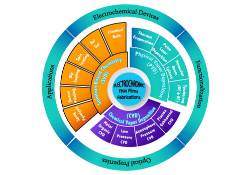
3. Electrochromic thin film deposition techniques
There are several deposition techniques available for the preparation of EC thin films as indicated in , of which most are summarized in subsequent sub-sections of Section 3. These techniques are classified on the basis of physical or chemical processes [Citation56]. The solution and gas-phase deposition methods are involved in chemical processes. Gas-phase methods comprise chemical vapor deposition (CVD) [Citation57], atomic layer epitaxy [Citation58], and atomic layer deposition (ALD) [Citation59]. Spray pyrolysis [Citation60], sol-gel [Citation61], spin [Citation62], and dip-coating [Citation63] processes are included in solution deposition methods. Physical processes include pulsed laser deposition [Citation64], physical vapor deposition (PVD) [Citation65], molecular beam epitaxy [Citation66], and magnetron sputtering [Citation67]. Additional techniques include: chemical bath deposition [Citation68], advanced reactive gas deposition [Citation69], electron beam evaporation [Citation70], vacuum evaporation [Citation71], and anodic oxidation [Citation72]. Each technique has its own advantages and disadvantages; a summarized paragraph and is added for the readers. (i) Physical vapor deposition (PVD): PVD is a renowned method for producing EC thin films. Following are some of the advantages and disadvantages of utilizing PVD for EC thin films. Advantages: PVD is a highly regulated method that yields high-purity films of homogeneous thickness and composition, which can increase EC performance. PVD may deposit a variety of materials such as metals, metal oxides, and alloys, allowing for customization of the EC characteristics of the thin film. PVD can be used to deposit homogeneous coatings on large substrates, ensuring that the substrate’s whole surface is covered uniformly. PVD is a relatively rapid method that can be used to fabricate EC thin films on a wide scale. PVD yields dense films, which can improve mechanical and chemical features. Disadvantages: PVD is an expensive technology that requires specialized equipment and knowledge, raising the entire cost of fabricating EC thin films. The size of the vacuum chamber limits the size of the substrate that can be coated using PVD, which can limit the size of the electrochromic device that can be constructed. Certain PVD processes demand high temperatures, which can limit the substrate selection and the EC film’s compatibility with other materials. PVD is often confined to fabricating thin films with thicknesses of a few micrometers or less, which limits the applications of ECDs. PVD produces films with a distinct morphology, which may be incompatible with some applications requiring specific surface features or structures [Citation73,Citation74]. (ii) Chemical vapor deposition (CVD): CVD is a promising method for producing EC thin films. The process includes the deposition of a thin coating onto a substrate via a gaseous chemical reaction. Although CVD has several advantages for producing EC thin films, it also has certain drawbacks. Advantages: CVD enables the deposition of a homogenous coating across a broad region of the substrate. This is especially crucial for EC thin films because uniformity ensures that the film responds to electrical stimuli in a consistent and predictable manner. CVD can be performed in a vacuum, ensuring that the deposited layer is devoid of impurities. This is critical for ECDs stability and lifetime. The thickness of the deposited layer may be precisely controlled using CVD. This is significant because an EC film’s thickness can impact its optical and electrochemical properties. CVD is a scalable process, which means it may be utilized to produce huge amounts of EC thin films at a reasonable cost. Disadvantages: To operate, CVD requires complex equipment and technical expertise. This can make the process difficult and costly to implement. The materials that can be deposited by CVD are limited. This can be a drawback for EC thin films since some materials have superior EC characteristics. Certain materials require high temperatures for deposition through CVD. Certain materials may not be able to tolerate the high temperatures required, limiting the substrates that can be employed. CVD involves the use of hazardous and flammable gases, which might be dangerous if not handled appropriately [Citation75,Citation76]. (iii) Solution based chemistry (SBC): EC thin films are commonly deposited using solution-based chemical processes. Following are some of the advantages and disadvantages of these techniques. Advantages: Solution-based deposition techniques are less costly than other deposition technologies such as sputtering and evaporation. Solution-based techniques are useful for industrial applications because they can deposit thin films over massive areas. These technologies are easily scalable, allowing for the production of a huge number of ECDs. Solution-based approaches provide substrate material diversity, allowing the deposition of thin films on a range of substrates such as glass, plastic, and metal. The properties of the deposited thin films, such as thickness, porosity, and composition, can be controlled using solution-based techniques. Disadvantages: Solution-based approaches achieve film thicknesses of a few micrometers, which may be insufficient for various applications. Solution-based deposition methods, such as sputtering and evaporation, require longer processing periods. Because of the uneven distribution of the solvents and solutes, solution-based techniques may yield inhomogeneous films. Because of the variance in film thickness across the substrate, achieving uniformity in the deposited films can be difficult. Solution-based approaches can yield lower-quality films than other techniques, such as sputtering and evaporation. The films’ defect density, adhesion strength, and electrical conductivity may be higher [Citation77–81].
Figure 2. Schematic illustration for the classification of thin-film deposition techniques.
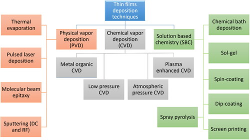
Table 1. Commonly used semiconducting (III–V, II–VI, and IV–VI) and metallic materials for film growth using metal-organic and organometallic precursors systems, methods, advantages, disadvantages and their uses.
In summary, the choice of deposition technique for the fabrication of EC thin films is determined by various aspects, including the desired film qualities, substrate compatibility, and cost concerns. It is difficult to say that one strategy is superior to others because each has advantages and limitations. As a result, the most appropriate technique should be chosen depending on the specific requirements of individual applications.
3.1. Physical vapor deposition
The constituents are changed from a solid phase to a vapor phase and transformed to a thin-film in a PVD process. The precursor is arranged in an active and entropic environment to change the particles to drip from its surface, therefore the thin-film solid is constantly directed toward a substrate surface. The active particles are attracted as they arrive at the strategically placed substrate. Also, the condensation of vaporized particles reaches lower energy substrates, due to which the thin films solid formed on them. The free motion of the gaseous particles is possible due to the vacuum in a deposition chamber. Because the particles struggle to adopt a conventional route in PVD, thin-films tend to grow directionally instead of conformably as commercially used in various fields, comprising manufacturing of thin-film solar panels [Citation82], polyethylene terephthalate film covered with aluminum for food packaging, and balloons [Citation83], and titanium nitride glazed cutting instruments for metalworking [Citation84,Citation85]. A typical PVD method is shown in [Citation86]. The following sub-headings briefly discussed various types of PVD.
Figure 3. Schematic of a typical physical deposition method setup Reproduced with permission from ref. [Citation86]. Copyright 2014, MDPI.
![Figure 3. Schematic of a typical physical deposition method setup Reproduced with permission from ref. [Citation86]. Copyright 2014, MDPI.](/cms/asset/bfcd70e7-4000-4415-9431-cb1ab484d0a7/ynan_a_2291619_f0003_c.jpg)
3.1.1. Thermal evaporation
A solid material is heated in a high vacuum chamber in thermal evaporation, leading to the production of evaporation inside the vacuum chamber as revealed in . This vaporized material form evaporation flow, which crosses the chamber and smashes the substrate, depositing to it as a coating or film [Citation87]. WO3 thin films are commonly produced by this technique. Besides WO3, thermal evaporation deposition can also be employed for thin film deposition of MoO3 and NiO [Citation88,Citation89].
Figure 4. Scheme of thermal evaporation deposition. Reproduced with permission from ref. [Citation87]. Copyright 2018, Elsevier.
![Figure 4. Scheme of thermal evaporation deposition. Reproduced with permission from ref. [Citation87]. Copyright 2018, Elsevier.](/cms/asset/3b914cda-5b95-4aac-89ce-4d8dbe37b214/ynan_a_2291619_f0004_c.jpg)
3.1.2. Pulsed laser deposition (PLD)
The high-energy pulsed-laser beam is directed within a vacuum compartment comprising the deposited source material. This material is vaporized from the target as a plasma cluster and finally thin films are placed on a substrate. The background gas or an ultra-high vacuum is necessary for the PLD process. Oxygen is also applied as background gas for the oxygenation of deposited films when depositing oxides. The primary setup of PLD is easy compared to many other deposition methods. Although, a quite complex physical process of laser-target interaction and the film development is involved as can be seen from [Citation90]. A series of energy conversions are involved in film formation by the PLD technique. The PLD method displayed a series of energy exchanges that results in evaporation, plasma creation, ablation, and exfoliation of particles [Citation91,Citation92]. Therefore, the surrounding vacuum would comprise numerous active forms such as, electrons, ions, particulates, clusters, atoms, molecules and molten globules before the deposition of particles on the substrate. The PLD technique is generally patterned with the Monte Carlo Techniques (MCT) due to the complex methods of thin-film development [Citation93].
Figure 5. Experimental setup of pulse-laser deposition technique for thin films synthesis. permission from ref. [Citation90] Copyright, 2019 MDPI.
![Figure 5. Experimental setup of pulse-laser deposition technique for thin films synthesis. permission from ref. [Citation90] Copyright, 2019 MDPI.](/cms/asset/f335e372-3a43-4686-bf20-4403b7b34348/ynan_a_2291619_f0005_c.jpg)
3.1.3. Molecular beam epitaxy
The epitaxy is made up of two words, epi and taxis (‘Epi’ stands for surface and ‘taxis’ means arrangement). Arthur and Alfred Cho made up molecular beam epitaxy (MBE) is a desirable method for depositing single crystals [Citation94]. For the deposition of thin-film in epitaxy, mono-crystalline substrates are used. The epitaxy is further categorized into two groups; (1) homo epitaxy thin film grown on the substrate surface of the same materials as that of thin-film, (2) hetero-epitaxy crystalline thin film developed over the crystalline substrate of different materials. The most important factor for epitaxial thin film formation is the structural characteristics between thin film materials and the substrate. Regular coordination should be developed between the substrate and thin films. Temperature is also a dominant factor for the epitaxial growth of thin films. Higher temperature led atoms to grow on favorable sites because of increased surface mobility [Citation95–99].
3.1.4. Sputtering
Sputtering is also an essential and outstanding process within PVD methods. It’s a non-thermal vaporization method in which due to the atomic collision, single atom from the targeted surface is removed by the bombardment of high energy ion. The source is produced by ion effect on the target, instead of thermal evaporation. It has surpassed other PVD methods in many cases with more features and operation like cleared attachment. Also, the distance between target and substrate is closer and thicker films can be produced. During the sputtering process, plasma accelerates gaseous ion which removes atoms from the target material’s surface by maintainable momentum transfer from bouncing particle bombardment with atomic-size. At low-pressure plasma of <0.67 Pa in a vacuum, the sputtered particles are in the line of sight and at a higher-pressure force of 0.67–4 Pa, the sputtered particles bounced or reflected from the surface of target through the gaseous phase and heated in advance, reaching the surface of substrate due to collisions. The principle of sputtering is employed to expel atoms from an electrode surface and as an etchant and for design characterization as well [Citation100–102]. The sputtering deposition can be applied as a generic term encompassing several procedures such as bias sputtering, diode sputtering (cathode or radio frequency), ion-beam sputtering, reactive sputtering, and magnetron sputtering [Citation103,Citation104] based on source and method. Variations in working pressure bring about by the power configuration of numerous power sources used in the sputtering deposition method. DC sputtering setup consists of a planar cathode and anode electrodes pair. Generally, the target material is arranged at the surface of cathode to be deposited while the substrate at the anode. Argon is used in the deposition chamber usually because of the larger mass to reduce cost relative to neon and helium and much energetic collision with the target material relative to krypton and xenon. Cathode (target material) and anode (substrate) are connected to a DC supply to maintain the beam discharging. These sustained beam discharges result in gaseous ions speeding to the target material, and the sputtering technique yields in film deposition on the substrate’s surface. Generally, metal is used as a conducting material in target in the DC sputtering system, subsequently; the glow discharge or flow of current is sustained among the electrodes [Citation105–107]. Sputtering involves radio frequency (RF) to escape charge construction over a few kinds of target materials which functions by alternating current flow in the vacuum surroundings at radio frequencies. A blocking capacitor is connected in series in RF sputtering between the cathode that would turn into a thin film and an anode. The power from the RF source transfers to the plasma discharge in a resistance-matching mesh in the capacitor. Ions sputtering of atoms with high energy as layering thin films over the surface are deposited at a stable frequency of 13.56 MHz when the cathode is targeted by a large voltage in a vacuum chamber. The optimization of power occurs for the generation of plasma for the target material, which is possible due to DC self-bias in the effect of the capacitor. RF sputtering provides many benefits like the potential of film growth on non-conducting (insulator) materials, power to maintain low pressure plasma at 0.13–2 Pa, of RF plasma diffusion during the total chamber, decreasing of race track corroding on the exposed surface of the point and power to washing the target materials from developing charge to decrease arcing effect, after each cycle [Citation108–110]. The electrons produce secondary electron due to ion bombardment usually radiated from the target surface and magnetron sputtering during the sputtering method, uses the magnetic field to bound the measure of the secondary electron to the surroundings of the target. The deposition rate can be higher with a better control over the ionization rate proficiency and current conveyed to the target by the arrangement and power of the magnetic field. A direct current (DC) can be employed for the deposition of conductive materials and a radio frequency (RF) power source is employed to deposit insulators [Citation111–114].
3.2. Chemical vapor deposition (CVD)
CVD process is used for depositing material from precursors, which could be volatile, reactive and/or decomposable on the exposed substrate surface to give a film by the gas phase. It has been applied in the semiconductor industry because of its suitability to form large area uniform surface coverage at 100–102 Torr and 350–800 °C [Citation115–117]. Variation of the method has been formulated via alterations in the starting materials, vaporization method, and choice of energy source for the deposition. The volatilization of the precursor is an important step in the CVD process. Average temperature is involved in a normal bubbler, for evaporation or sublimation in precursors for enough vapor pressure. Enough thermal constancy is shown in precursors such that neither gas-phase nor decomposition reactions consume the precursor earlier it attains the substrate. Hence, to alleviate the volatilization and vapor phase transport, there has been considerable power to orient the physical characteristics of precursors.
3.2.1. Metal-organic chemical vapor deposition (MOCVD)
Employing metal organics as precursors makes this variation of CVD. The metal organics are organic radicals in which the metal atoms are bonded to in a compound. Organometallics have one or more direct metal-carbon covalent linkage. The name MOCVD further evolved to organometallic CVD (OMCVD) because of the use of organometallic precursors. MOCVD can be employed to deposit epitaxial, amorphous, and polycrystalline films for large variation of materials. describe methods of metal-organic and organometallic precursor’s that are usually employed to develop III–V, II–VI, and IV–VI semiconducting, dielectric films, and their uses.
3.2.2. Low pressure chemical vapor deposition (LPCVD)
A simple LPCVD system usually consist of a hot-wall tube furnace reactor of diffusion-type (other than a plasma reactor), a gas flow measuring system, a substrate vessel for vertically orienting wafers, a discharge provision, and a vacuum pump [Citation146,Citation147]. shows a sketch of an LPCVD method [Citation148]. Fused silica made heavy-walled round tube in the reaction chamber designed for vacuum application and standard wire-wound resistance elements for heating. A tight stainless-steel cap is used in the entry side of the tube with a loading door, water cooling, gas inlets, and the withdrawal part is compactly linked to a trap water-cooled and filter for condensation and holding supplementary derivatives. Oxide films in LPCVD are heated at low temperature (range 350–450 °C), especially fused quartz or stainless steel made slotted tube has been projected to increase the gas flow regularity in the reactor [Citation147,Citation149]. Wafer vessels or boats are employed to consider substrate wafers with a minimal hindrance in order to enhance film regularity. Usually, perpendicularly placed wafers are used typically at 3–5 mm spacing’s to the gas stream for high-temperature LPCVD, they facing vertically stand to the exit of the tube reactor. Typically, single positioned of more than 100 wafers loads in the spaces, or back-to-back of 200 wafers are used. Wafer contamination is avoided while loading and unloading wafers at the gas entrance side of the tube. A device such as a rotameter, for any flow measurement with pressure-sensitivity, the sensor control valve should be positioned downstream. The pumping method has a leading influence in this LPCVD reactor process. Many LPCVD processes require a 15-to-50 ft3/min-capacity of single- or dual-stage mechanical vacuum pumps that swiftly process the 50–500 cm3/min standard runs at 0–5-torr pressure, available commercially. Certain processes such as 450 °C treated SiO2 and 900 °C treated Si3N4 might require a greater gas flow and/or lesser pressures. When a blower employed as a booster pump in an efficient way to enhance both system’s handling LP capability and capacity between the mechanical pump and the reactor. The blower permits to control the most important variable i.e. reactor pressure using a varied speed motor, either the employ of an automatic feedback loop manual or amendment of the motor speed from the pressure sensor output [Citation150]. The rate of film deposition is affected by differences in pump capacity and the wafer load changes the ambient of downstream gas, which in turn upsets the degree of reorientation of the temperature sketch. For cautious attention of safe low-maintenance process, vacuum pumping might contain flammable, explosive, poisonous, and corrosive gases. Recently two papers have been published conversing different kinds of pumps, fittings, fluids pump, and safe working methods for processes involving a low-pressure [Citation147,Citation151]. Two kinds of LPCVD reactors were shown where the wafer substrates were not placed in vertically. The cylindrical-geometry RF-heated reactor is typically employed for silicon epitaxy, basically the identical to the cold-wall barrel reactor, where the wafers are placed on the indirectly placed susceptor slabs (rotating) [Citation152]. Whereas, the other is a parallel wafer covering form permitting a capability of up to 100 wafers for high-volume as a new design reactor with cheap silicon epitaxy with susceptor disks rotating, a plurality of stirring gas jets performing as dispersion method for gas. The apparatus has been planned for controlling under reduced pressure, although usually controlled at atmospheric pressure [Citation153].
Figure 6. Schematic illustration of an LPCVD system. Reproduced with permission from ref. [Citation148]. Copyright 2014, Hindawi.
![Figure 6. Schematic illustration of an LPCVD system. Reproduced with permission from ref. [Citation148]. Copyright 2014, Hindawi.](/cms/asset/95af109a-6e7a-41b1-b4c8-b5fece4c7f34/ynan_a_2291619_f0006_c.jpg)
3.2.3. Atmospheric pressure chemical vapor deposition (APCVD)
This CVD method is employed for gaseous precursors onto an appropriate substrate for deposition of coatings indicated in [Citation154]. Moreover, the pressure of the reaction chamber in the APCVD technique is preferably at one atmosphere of pressure or close to atmospheric pressure. Volatile liquids or low-melting solids are used as precursors driven by the carrier gas to the reaction chamber. Two kind of processes such as homogeneous and heterogeneous occur inside the reaction vessel in the vapor phase and at the vapor solid surface interface. In different CVD methods, single or dual source precursors can be used. The entire group of elements essential for consecutive coating making are present in single-source precursors. APCVD method uses a compatible precursor, i.e. volatile, and consequently must react for the formation of the desired material [Citation116,Citation155]. In general, a single-source precursor must be simple, volatile, and comprise the suitable atoms necessary. Ideally, the precursor stoichiometry should match with that of the final coating [Citation156]. Instead, multiple precursors are involved in the synthesis of coatings with the interaction of dual-source precursors. In general, dual-source precursors are more cost-efficient and additionally simpler to their single source equals for CVD on glass. Carrier gas should deliver the gas phase precursors for the construction of thin films is vital separately. N2, He, or Ar are the most common carrier gases, particularly when extremely reactive pyrophoric reactants are employed and instead, most of reactions involve energy from the carrier gas, e.g. H2 or O2 [Citation116,Citation155,Citation157].
Figure 7. Schematic illustration of an APCVD reactor. Reproduce with permission from ref. [Citation154]. Copyright 2015, Elsevier.
![Figure 7. Schematic illustration of an APCVD reactor. Reproduce with permission from ref. [Citation154]. Copyright 2015, Elsevier.](/cms/asset/11025d05-cab1-4b99-844d-81329892a89c/ynan_a_2291619_f0007_c.jpg)
3.2.4. Plasma enhanced chemical vapor deposition (PECVD)
This method involves the growth of a thin film of a solid-state from a gaseous state. Plasma is produced by the chemical reaction which results in the production of a film on the desired substrate. Most of the CVD methods use thermal energy, although an electrical source of energy is used in PECVD to produce plasma and tolerate the reaction method. Chemically active ions are produced to initiate homogeneous process to use electrical energy and radicals that participate in heterogeneous processes, which would facilitate layer development on the substrate. Compared to thermal CVD methods, low temperature deposition is the key advantage of PECVD which is suitable for temperature sensitive materials [Citation158–160]. Numerous new reaction routes open up for the deposition by using plasma to significantly stimulate the gas-phase chemistry.
3.3. Solution based chemistry (SBC)
3.3.1. Chemical bath deposition (CBD)
This solution growth method is mostly applied to films growth of metal chalcogenide. It is also called controlled precipitation, or chemical deposition method. It is sometimes considered as liquid phase parallel of the popular chemical vapor deposition. At low temperature (30–80 °C), reaction occurs between the dissolved precursors in solution. Precursor of sulfide family are commonly employed, which include thiourea, thioacetamide, thiosulphate, and sodium sulfide. Whereas, metallic precursors are obtained by forming metal complexed ions having ammonia ligands. The stimulating point between CBD and spray pyrolysis is that the same solvent dissolved precursors (thiourea and thioacetamide and metal salts) are employed for the sulfide deposition [Citation161]. In the case of CBD, an impulsive process from the liquid phase is probable, so the solution chemistry is selected, contrary to spray pyrolysis where the reaction requires a much higher temperature (300–600 °C) to procedure due to different solution chemistry and thus occurring from the vapor phase. This method is currently drawing significant consideration as it needs simple instruments like a hot plate with a magnetic stirrer and does not need advanced or expensive equipment like a vacuum system or furnace. The preliminary chemicals are low-cost and usually accessible. A great number of substrates can be coated in a CBD method in one cycle. The substrates electrical conductivity is not the requirement. The solution which has free access to any insoluble surface will be an appropriate substrate for deposition. The corrosion and oxidation of metallic substrates are avoided by low-temperature deposition. Since the basic assembly is ions in place of atoms, a uniform and pin-hole-free deposit is easily obtained in the chemical deposition. Easily controllable preparative parameters result in better orientations and improved grain structure. The status of CBD has been discussed in several review papers [Citation162–166].
3.3.2. Sol-gel method
In this method, molecular precursors undergo hydrolysis and condensation process under suitable circumstances. The solid phase network is presently formed by two chemical ways: alkoxides metals dissolved in organic solvents via a metal-organic route and metal salts (chlorides, nitrates, sulfides, etc.) dissolved in aqueous solutions through inorganic path. Most variable precursors are the alkoxides. To fabricate hybrid materials, it is possible to apply mixed inorganic and organic precursors as well. The solution of a metal alkoxide M(OR)n precursor that is strongly alcoholic is generally used in the sol-gel process, containing ‘R’ alkyl group. The hydroxyl groups are obtained in a three-dimensional system through hydrolysis of metal alkoxides, followed by their poly-condensation. Simultaneously, by-products of alcohol and water of low molecular weight are generated through the reactions of hydrolysis and poly-condensation. Nucleophilic substitution (SN) initiates both reactions, comprising these steps: nucleophilic addition (AN), transfer of proton within the transition states, and the proton elimination of species (alcohol, water). A tetrahedral SiO2 or a MOx network formation takes place in the process [Citation167]. For metal alkoxides, the sol-gel process can be carried out without using a catalyst and due to its high reactivity. The condensed species result in the formation of oligomers, gels, colloids, or precipitates. Sol’s formation occurs as a result of Oxo polymers and colloidal particles that can be densified, gelled, and dried to obtain films and powders. shows a schematic illustration of different yields of the sol-gel method. Various products obtained in the sol-gel method are shown in . Several different end products can be obtained, dependent on the intermediary methods (coating, gelling, precipitating, etc.), when precursor material transforms to sol during hydrolysis and poly-condensation. For inorganic precursors, the chemical modification of alkoxides controls the polymerization or condensation rate (poly-condensation) with ligands including acetylacetone. The hydrolysis rate and condensation steps could be adequate by using complexing ligands in the sol-gel process. A xerogel with a large surface area, densified form, and sponginess can be obtained when dried under normal conditions. The gel state directly form monoliths, films, fibers, or powders, depending on the post-processing as revealed in [Citation168].
Figure 8. Different products obtained via sol-gel routes. Reproduced with permission from ref. [Citation168]. Copyright 2017, Elsevier.
![Figure 8. Different products obtained via sol-gel routes. Reproduced with permission from ref. [Citation168]. Copyright 2017, Elsevier.](/cms/asset/f6e0aa12-d49e-47e4-81c3-d054c359eac8/ynan_a_2291619_f0008_c.jpg)
3.3.3. Spin coating
This is the most renowned method both within academia and industry for homogeneous layers, because of the well-known processes resulting in thin film formation during deposition. The various steps in this process are shown in . The solution is first dropped on top of the substrate fixed by a vacuum pump on the spin coater. The solution must cover the substrate surface completely earlier to the spinning. The spin coater speeds up to a great RPM and is kept at the same speed for pre-fixed time duration and the substrate is coated with the solution [Citation169]. Combining the liquid flow and evaporation, the thin film resulted when the spinning is finished by completion. Due to various types of precursors employed, heating, or UV treatment, some extra steps are required for the thin films to be formed. The thin films with thicknesses control can be produced, as spin coating processes have undertaken abundant experimentation and modeling. The film thickness follows a common rule for most precursor solutions concerning spin speed and duration. The simple estimate of variations in the speed of spin and duration belonging thickness of the film. There is a relative decrease in thickness of the as-deposited thin film as both speed and duration rise [Citation170]. The range of duration/acceleration/speed values needed for producing the greatest quality, tests are done on fresh solution precursors to control a variety of as-deposited thin film thicknesses. The spin coating involved modeling of the processes which depend on the dynamics of fluid and contact with surface. The operating procedures are adequately detailed for complete understanding of process elsewhere [Citation171–174]. A powerful relationship has been demonstrated between as-grown thin film thickness with spin-coating parameters by modeling a feature of a solution for example viscosity, density, shear-thinning, and the rates of evaporation. Interestingly, a cross-over point analysis can also be employed to control the changes in thin-film thickness during the deposition process. The thickness of a film is controlled by the speed of spin and liquid flow (by acceleration). The evaporation of the precursor solution is the second dominating force. For several materials explained in the previous section, a higher rate of evaporation would mainly affect the morphology of film relative to different solutions, mainly aqueous ones. When a ramp time is longer, it potentially forces the cross-over point to happen earlier in the acceleration step. This may result in adversely affecting the thickness, morphology and consistency of film. It is more challenging for complex metal oxide, to obtain thin films only from precursors without the need for further improvement by post spin steps including exposure to water, air, heat, etc. Uniform thin films of most complex oxides grown still depend on vacuum-based deposition techniques. The mixtures for final coating of more complex composition are delivered in solution-based chemistry. The variable nature of spin coating is sensitive to wetting, evaporation, solidification, and changes in volume which are operative and often non-linear. New models are required for the control of spin coating that is precise for the precursors with a beneficial formation to suitably exact in the spin coating information to retain probability in consistency. Hence, popularity of spin coating for film deposition within academic and industrial environments as a solution-processable route is ensured due to its accessibility, cost efficiency, and uniformity of deposited thin films [Citation169].
Figure 9. Schematic illustration of the steps involved in spin coating to obtain thin films Reproduced with permission from ref. [Citation169]. Copyright 2016, Wiley.
![Figure 9. Schematic illustration of the steps involved in spin coating to obtain thin films Reproduced with permission from ref. [Citation169]. Copyright 2016, Wiley.](/cms/asset/86e4658c-bbdb-4255-ba2e-df6cf11ec831/ynan_a_2291619_f0009_c.jpg)
3.3.4. Dip coating
This process is becoming attractive for film deposition, especially for irregular surfaces. However, it has no wide applications in the semiconductor industry. Compared to spin-coating, dip-coating comes with a compromise over the choice for materials, particularly in measure because of the quantity of precursor needed in the solution tank. The research is under process so that the facts of the procedure can be extended and employed for active depositions. However thin film formation mechanism is understood, and divided for numerous solutions, polymers, and composite liquid-borne species. Dip-coating method has the advantage of predictable variations to the deposition method to obtain complex and varied surface morphologies for thin films. The experimental set up for a standard dip-coating technique is displayed in [Citation175]. The substrate is first dipped into a precursor solution, and then removed. The liquid film is initially formed which changes to a solid film. The solid thin film changed to its final phase by post-processing steps such as thermal treatment for tuning of its property. Multiple and successive deposition steps are carried out to obtain a multi-layered thin film, where thickness of each consecutive layer is slightly higher than the preceding. The thickness of a film is mainly controlled through the withdrawal speed. The thickness can also be controlled by varying deposition temperature and the concentration of precursor solution. In all circumstances, an interactive cause-effect structure is a setup, by which increasing concentration distresses the physical characteristics of the deposit. Brinker et al. made a schematic, which displays the methods taking part in making thin film formation in a regular state method [Citation63,Citation176]. The withdrawing drying line velocity equals the extraction speed in a steady-state method. Different forces interact for forming the thin films during steady-state dip-coating. The forces comprise gravity, inertial forces, viscous dragging, and meniscus surface tension and so on. It is possible through experimental design and examination to employ understanding of the precursor materials as well as solution to plan the thickness of a thin film. Landau et al. introduced a facile way to deposit a film on a substrate highlighting the impact of the viscosity as well as the surface tension related to the material to assure an instantons liquid film growth through a stable removal speed [Citation177]. Hence, the liquid is the solubilized precursor solution, which finally withstands chemical alteration. The liquid height (h0) is achieved by the removal speed (U0), viscosity (η), liquid density (ρ), gravity (g), and surface tension (γ) detected by the Landau-Levich model such that
(1)
(1)
Figure 10. Schematic of dip-coating technique to form thin films. Reproduced with permission from ref. [Citation175]. Copyright 2019, MDPI.
![Figure 10. Schematic of dip-coating technique to form thin films. Reproduced with permission from ref. [Citation175]. Copyright 2019, MDPI.](/cms/asset/a02b825a-db97-46c7-ae64-0d8a291bcb13/ynan_a_2291619_f0010_c.jpg)
In this liquid film method, the solid thin film is deposited via evaporation, gelation, and solidification. Consequently, the obtained thin solid film was regulated by operating the liquid film thickness. When the thickness of film/material via the characteristics of the solution is to be designed through the Landau-Levich model, other procedures must be taken into consideration for a comprehensive explanation of the material used for thin film for optimum thickness. However, because of chemical variations within the liquid coating materials, other factors may also vary for precursors, such as energies of the substrate surface and wetting angle. The film thickness can vary with withdrawal speed for different precursor’s solution. In this case, each of the solutions used with various acid/polymer additives and ethanol solvent for different silica and titania family of materials employed for synthesizing the thin solid film. The graph of withdrawal speed versus thickness underlines a turnaround mode afterward a certain reference when further increase in speed of deposition enhances thickness of film. Faustini et al. mentioned that this phenomenon is due to the alteration in the procedures that control the development and solidification of thin-film because of capillary or draining interactions acting on the film [Citation178]. They pointed out that both the binary phases capillary/evaporation and draining/evaporation procedure led to the formation of the film regardless of removal speeds (slow rate or fast rate) [Citation179]. For the draining procedure, where the Landau-Levich model governs in fast rate deposition, the capillary forces are small enough because of the oppose meniscus properties as a result of the high withdrawal speed. The surface of the substrate is wetted by the solution and through the draining step the extra material is drained; the solid thin film made after evaporation has taken place. Whereas, for the capillary process (slow rate deposition), a thin-film formation is governed by the rate of evaporation of the solution during slow withdrawal. The capillary feeding takes place during slow withdrawal from the surface tension of precursor. Hence gravity and viscosity factors of associated with rates of evaporation of solutions have great influence on the film thickness [Citation171]. Therefore, an intricately linked interplay of draining, capillary, and evaporation forces at the intermediate withdrawal speeds, dominate the film thickness. The effects of solution temperature and the precursor concentration with variation to the polymer supporting the deposition were also considered by Faustini and his co-workers [Citation178]. A significant matter must be taken into the description for numerous dip-coating depositions when employing mixtures of shared precursor solutions with different constituents. While selecting a withdrawal rate for different material, the chemical properties of the material within the solution becomes crucial. As different volatile additives with large alterations in the evaporation rate can take a different drying line, following the maximum rate of evaporation. If the solutions with dissimilar evaporation are used, film deposition may result staggered and lacking in uniformity. As one material evaporates previous to the other, the staggered deposition takes place as observed by Nishida and co-workers. A strong activity was observed because of higher liquid content close to the drying line relative to the aqueous content of the last precursor [Citation171,Citation180]. For a mixture of a solution comprised of various materials, each of the ingredients are accounted mostly those connecting to evaporation and wetting aptitude. For instance, if the solution comprises of both comparatively a unstable solvent, for example EtOH or IPA and non-volatile H2O, it can show evaporation of the solvent earlier than the creation of the liquid film and following solid thin film [Citation180,Citation181].
3.3.5. Screen printing
This altering method has been of all the techniques used for fabrication of two-dimensional patterns at the beginning of twentieth century [Citation182]. The basic principle of screen printing for thin films preparation is displayed in [Citation183]. The squeegee travels and hits the ink paste contrary to the screen. The screen is typically prepared of a stainless steel or porous fabric. The probable pattern, i.e. the stencil, is photochemically or physically demarcated in the grid [Citation184]. The efficient working of the printing process is affected and determined mainly by the viscosity of the ink and wetting of the substrate. The resolution of the printed patterns can be limited by the dimensions of mesh, i.e. a thickness of about 30–385 µm for polyester and about 40–215 µm for stainless steel wires, respectively can be achieved for a 30–200 threads/cm with meshing [Citation185]. Screen printing can be classified based on how it is built with substantial alterations of the two methods, i.e. rotary screen printing and flat-bed screen printing. For large-area printing (up to 10 m2), flat-bed screen printing is suitable due to the facile rearranging between prints, low-cost preparation of the mask and probability of building each print separately. Whereas, in rotary screen printing, a covered rotating cylinder holds the precursor ink. The cover is more costly in this method, though this technique is in fact close to roll-to-roll printing method for its high speed, sharp definition of edges, and wet thickness [Citation186]. It is employed in the screen printing of active layers for fuel cells, solar cells; thin-film based organic field effect transistors (OFET) [Citation123,Citation182,Citation187–189]. The liquid inks used for screen printing are mostly categorized with shear weakening features with viscosity between 0.05 and 5 Pa. Ideally, inks with a high rest viscosity and at low shear viscosity, and rapid viscosity retrieval are preferred. A solid-surface needs an extensive retrieval time to attain a smooth surface when printing there by permitting the ink to flow and attain an even coating after printing. When printing of lines or solid areas, the stream of ink via the screen can cause deficiencies. Sometimes, the ink may drift over and around the single threads of the mesh. Local incomplete pattern happens, if the ink flow is inadequate which consequences in a wonder called mesh pattern (an even patterning of line width). Function of the printing circumstances and the ink features depend on the amount of mesh pattern [Citation190]. Screen printing profits from its easiness, likeness with the change of organic inks, and printing capability ambient pressure. This permits good reliable low-cost printing on plastic substrates [Citation191]. Moreover, in variation with gravure printing, a wet layer of thickness between 10 and 500 µm and consequently a dry thick film is essentially allowed in screen printing technique. This can be helpful for printing of high conductivity electrodes [Citation186]. However, a comparatively low resolution (>75 µm) is a drawback for successful application in the manufacturing with great feature size displays. The active layers with good control over morphology and film thickness can be difficult to obtain with high precision. Additional difficulty during printing is the disclosure of the ink to the atmosphere. For an industrial procedure, it is necessary that during open time of numerous hours the ink should still retain its wetness and viscosity. If volatile solvents are employed it debased the definition of the printed pattern because of dry up in the screen printing mask [Citation182].
Figure 11. Schematic illustration of the screen-printing technique for thin films preparation. Reproduced with permission from ref. [Citation183]. Copyright 2011, MDPI.
![Figure 11. Schematic illustration of the screen-printing technique for thin films preparation. Reproduced with permission from ref. [Citation183]. Copyright 2011, MDPI.](/cms/asset/544006a3-d0b1-4c88-8fae-55a8e56db83b/ynan_a_2291619_f0011_c.jpg)
3.3.6. Spray pyrolysis technique
Spray pyrolysis technique (SPT) is categorized as a solution-supported chemistry grounded on the character of the deposition. The deposition of film solution-based methods is becoming more popular [Citation189]. Great purity at low cost, starting from simply accessible materials is produced in solution-based methods. Varieties of the thin film are depositing in SPT. Using SPT, films with a uniform thickness of very thin layers can be coated on a large area [Citation192]. The thin and thick films, porous films, dense films, multilayered films, ceramic, and powders can be deposit in this technique [Citation193]. Any composition of films can be prepared in this process [Citation98]. It is also useful for high-quality products in the control of target compositions. It permits insufficient precursor treatments for large surface deposition [Citation194]. High-quality films can be obtained by optimization of the preparation conditions. Spray rate, substrate temperature, and concentration, etc., are included in such preparatory conditions. SPT involves a heated surface in spraying solutions of the film [Citation195]. Thereafter, the film segments rejoin forming a chemical compound. The chemical reactants are designated so that unwanted yields pyrolytically deteriorate at the deposition temperature [Citation97]. The experimental set-up of the SPT technique is demonstrated in . SPT apparatus comprise the precursor solution, substrate heat source, an atomizer, and temperature controller [Citation196]. The normally employed atomizers are ultrasonic, electrostatic [Citation197], and air blast [Citation198]. Ultrasonic frequencies are used in ultrasonic atomizers for fine atomization to yield a short wavelength. To take place atomization electrostatic atomizers uncover the liquid to a high electric field. The liquid is exposed to a stream of air-by-air blast atomizers. SPT is a useful method because it is a simple method for the deposition of metal oxides with low apparatus cost, and needs slight preservation. Compared to the vacuum equipment, it does not consume much power. Also, after using SPT for deposition, electricity is not required. The process parameters largely affect the superiority and features of the deposited films. The temperature of the substrate surface disturbs the output of the films. A rougher and porous film is produced with higher substrate temperatures, but low temperatures give a fractured film. Deposition temperature also determines the physical properties, crystallinity, and texture of deposited film [Citation199]. Morphology and features of the deposited film are also affected by precursor solution [Citation200]. SPT is classified into four methods through reaction type [Citation201]. Process 1 requires the droplet occupying on the surface allowing the solid to react and dry as the solvent evaporates. In Process 2, the droplet creates interaction with the surface just after the solvent evaporates. Impinges of dry solid on it allow for breakdown. Procedure 3 is known as actual chemical vapor deposition. As the droplet reaches the substrate, the solvent vaporizes. To bring about the heterogeneous reaction when solids melt and vaporize by diffusing these vapors into the substrates. Process 4 occurs in the vapor state. The droplet has four possible ways before beating the substrate regardless of temperature or initial droplet size [Citation202].
Figure 12. Experimental set-up of the spray pyrolysis technique. Reproduced with permission from ref. [Citation196]. Copyright 2004, Elsevier.
![Figure 12. Experimental set-up of the spray pyrolysis technique. Reproduced with permission from ref. [Citation196]. Copyright 2004, Elsevier.](/cms/asset/4d6b1d62-59f7-4a1e-b41b-381c9734382c/ynan_a_2291619_f0012_b.jpg)
4. Functionalization of electrochromic thin films
The surface of EC thin films is modified to introduce certain functional groups during functionalization. This method enables us to induce and impart additional features, as well as enhance existing properties of materials. This can be accomplished through the use of several strategies such as: (i) Chemical modification: In this approach, the EC thin film is treated with active chemical substances capable of introducing functional groups into the surface. (ii) Electrochemical modification: An electrochemical method is used to introduce functional groups onto the surface of the EC thin film. For instance, anodization can be used to add functional groups to the surface of conducting polymer films. (iii) Plasma treatment: In this process, the EC thin films are subjected to a plasma, which can add functional groups onto the surface. (iv) Self-assembly: In this strategy, certain molecules or nanoparticles are to be self-assembled on the surface of EC thin films, which can lead to the improvement of the material’s existing properties due to the introduction of some active functional groups onto the surface. Based on the materials available and our understanding, it is obvious that functionalizing EC thin films can provide additional qualities such as higher stability, improved functionality, and enhanced performance, making them more useful in a wide range of applications. The choice of functionalization technique depends on the specific requirements of the application and the desired functional groups [Citation203–205]. More detail with selected examples can be seen from subsequent sections.
4.1. Viologen electrochromism and polymeric viologen systems
The herbicides salts called quaternized 4,4/-bipyridine are formed on a great scale. The complete accessibility of 4, 40-bipyridine and the simplicity of changing quaternizing agent’s nature has granted thorough investigation into the EC features of these ‘viologens’ [Citation206]. The 1, 1/-di-methyl-4, 4/-bipyridilium, prototype viologen is famous as methyl viologen (MV), and is called ‘substituent’ viologen with other simple symmetrical bipyridilium types. Out of the three well-known viologen redox states as indicated in , the maximum steady is di-cation and in unadulterated form is colorless otherwise with the counter anion, an optical charge transfer takes place. The radical cation results due to the reductive electron transfer to the viologen di-cation. The stability of which is accessible to the delocalization of the radical electron all over the p-framework of the bipyridyl nucleus, the 1 and 10 substituents normally transport fraction of the charges. The viologen radical cations are extremely colored, having high molar absorption coefficients, because of the optical charge transfer taking place between the (formally) C1 and zero-valent nitrogen. The ideal case of nitrogen replacements in viologens to reach the proper molecular orbital energy levels can principally permit a color choice of the radical cation. For instance, alkyl groups excite a blue/violet color while the radical cation of 1,1/-bis(4-cyanophenyl)-4,4/-bipyridilium (cyanophenyl paraquat, ‘CPQ’) [Citation207] in solution (acetonitrile) displays a deep green color (83,300 dm3 mol−1 cm−1 at the λmax (674 nm)). The color effectiveness showed by di-reduced viologens as indicated in , is weak because no internal transition or optical charge transfer connected to wavelengths in the visible range is obtainable. Schoot et al. [Citation208] described the first electrochromic exhibition employing viologens (of the Philips Laboratories) in 1973. In 1970 Philips had filed Dutch patents [Citation209] for 1,1/-diheptyl-4,4/-bipyridilium as the electrochromic agents, whereas, cyanophenyl paraquat was untested by ICI in 1971 [Citation210]. At this time, Barclay’s group at Independent Business Machines (IBM) and Texas Instruments in Dallas investigated shows based on the heptyl viologen [Citation211]. However, their effort did not get much attention during this time [Citation212]. A 64 × 64 pixel incorporated show with less than ten levels of gray tone on a 1-in2size silicon chip, proficient in displaying reasonably elaborated images, was described [Citation213]. These exhibitions did not popularize more due to LCD rivalry. However, they still offer a size benefit for larger sized instruments. Employing a novel nano-structured type EC organic/inorganic hybrid organism, ‘paper-quality’ railway terminal data long-term data shows are fairly near to commercialization, where the uneven surface of a large area porous oxide film is involved in EC groups including phosphonated viologens and phenothiazine molecules [Citation214,Citation215]. Usually, in these a transparent conductor electrode is deposited and consists of systems of integrated nanomaterials of semi-conducting or conducting metal oxide. Electrons injection takes place into the conduction band of the semi-conductor on relating a negative potential reducing the absorbed molecule to allow color changes to take place. The method is inverted by giving a positive potential. Gentex’s commercialized a noteworthy interior ‘Night Vision Safety’ (NVS) mirror with automatic-dimming utilizing viologen electrochromism [Citation17]. A cell of two electrodes was formed, a solvent holding two electroactive chemical materials functioning as EC materials and supporting electrolyte between ITO-glass surface and the reflective metal surface. Two electroactive chemical species contain a replaced (cationic) viologen. One of these two works as the cathodic, and the other one a phenylene diamine negatively charged EC material acts as the anodically coloring. When the mirror is switched on, these species will transfer to their respective electrodes. These are then transferred into the solution where the respective products after the multiple EC color operation meets and results in the original uncolored species. Due to the loss of the colored electroactive species, these types of electrochromism then use a low current for detachment of the colored elective active species. Bleaching results due to homogeneous electrons transfer of short or open circuit in the bulk of the solution. The sharp control system device is also vital in addition to the EC process. The bright incident light is detected by a photosensitive detector. Though, it can be stimulated in the daylight as well, which may cause an undesirable mirror darkening. The solution is provided by positioning a second detector which is forward looking. The second detector disables the function of first detector upon detecting daylight.
Figure 13. The three well-known redox states of viologens, displaying the two consecutive reactions of electron transfer Reproduced with permission from ref. [Citation216]. Elsevier 2006.
![Figure 13. The three well-known redox states of viologens, displaying the two consecutive reactions of electron transfer Reproduced with permission from ref. [Citation216]. Elsevier 2006.](/cms/asset/05580a77-c9bf-4d46-adae-50ec6b301715/ynan_a_2291619_f0013_b.jpg)
4.2. Tungsten oxide/multi-Walled carbon nanotube hybrids
Nanostructured WO3 films mixed multiwall carbon nanotubes (MWNTs) have been organized by a Sol-gel process, with Peroxotungstic acid. Lithium dodecyl sulfate (LDS) (1%) was introduced to the MWCNT colloidal suspension and ultrasonicated. MWCNTs rendered the mechanical support of electrochromic films, with improved conductivity, and a considerable enhancement of the diffusion rate of lithium ions. However, the long (380 s) bleaching time was detected as the Li ions got captured in the WO3-MWCNT hybrid network. By employing only low quantity of (0.1–0.2 wt. %) carbon nanotube, the superiority and EC features of the WO3-MWCNT hybrid remained established greatly enhanced [Citation217]. The better features such as very firm reply times were attributed to the extremely porous amorphous structure of the composite.
4.3. Metal oxides
Since the discovery of electrochromism, research and development has been ongoing on the EC materials and their uses [Citation21]. Recently, research interest has grown towards EC oxides. Primarily distinct sorts of EC oxides are those called cathodic color and anodic under ion insertion and extraction, respectively [Citation218]. Application of voltage between the EC films cause transport of ions. One direction makes both of these films’ colors, and makes both of them bleached by carrying ions in the other direction. This can be named as the ‘‘rocking chair’’ method similar to one used for the lithium battery technology. Tungsten oxides are the mostly used as cathodic EC oxides [Citation7,Citation219]. The schematic reaction can be outlined as the equation beneath:
(2)
(2)
This is the proton insertion/extraction case. Tungsten oxide has drawn tremendous attention recently, for pseudo-capacitor and EC applications [Citation220,Citation221]. For example, Yang et al. developed multi-role glass windows that integrate electrochromism and energy storage employing film electrodes of WO3 as shown in [Citation222]. Although, films of WO3 displayed large specific capacitance of 639.8 F g−1, the color altered from transparent to the deep blue exhibiting its outstanding energy storage and electrochromism feature with a sharp reduction in transmittance from 91.3 to 15.1% at a 633 nm wavelength and at a voltage of 0.6 V (vs. Ag/AgCl). The WO3 electrode color efficiency was 54.8 cm2 C1. Further, a prototype pseudo-capacitive glass window (15 cm x 15 cm) with WO3 film was produced at a large scale. Afterwards, the charge storage method of film for WO3 was examined quantitatively [Citation223]. Significantly, WO3 film normally stands from ion-trapping induced degeneration of the optical modulation and the cycle reversibility on extended cation-ion exchange. Although, this consequence can be positively removed by the constant current driven de-trapping, allowing for a common foundation for emerging and plotting higher EC instruments [Citation224]. This smart pseudo-capacitive glass window displays pronounced capacity in working as EC-window and simultaneously driving electronic devices. Recently, Xie et al. fabricated a self-powered smart EC-window with adjustable transmittance directed through dye sensitized solar-cells, that can also react as a photo charged supercapacitor with elevated real capacitance and color variations [Citation225]. Another cathodic EC oxide is Niobium oxide (Nb2O5), and the charge-storage mechanism of pseudo-capacitance is classified as an essential merit of Nb2O5 that eases the electrode for capacitive storage-devices [Citation226,Citation227]. Milliron et al. originated a synthetic arrangement for comprising Nb2O5 nanocrystals by attaining the procedure of adding tin-doped indium-oxide nanocrystals into the Nb2O5 glass, thinking of a novel amorphous structure [Citation228]. The calculated coloration competence was about 30 cm2 C1 at 500 nm and the subsequent material offered a hitherto unrealized optical-switching exercise with a potential to assist in harvesting of solar radiation transmittance effectively between gaps. TiO2 is used favorably as cathodic electrochromism material as the unoccupied sites fashioned by the shared edges are sufficiently great to hold protons and Li+-ions [Citation229,Citation230]. Giannuzzi et al. prepared, and employed new anisotropic TiO2 (B) nanocrystals to produce extremely effective electrodes for Li storage [Citation231]. The prominent lithiation/de-lithiation potentiality was used to make the ECDs that exposed a magnificent coloration proficiency of 130 cm2 C1 at a wavelength of 800 nm at employed voltage of 1.5 V, and a tremendously rapid EC-switch (coloration time 5 s). The schematic reaction of nickel oxide based anodic electrochromism oxides can be concise as:
(3)
(3)
Figure 14. Cathodic electrochromism oxides and their application in multifunctional combining energy storage and the electrochromism via the WO3 films electrode (a) cross-section SEM of glass windows device (b) electrochemical performance by IV voltammetry (c) optical images. Adapted from Ref. [Citation222] with permission. Copyright 2014, John Wiley and Sons. (d) The optical transmittance spectra of NiO thin films obtained via the chemical-bath deposition. Adapted from reference [Citation68] with permission. Copyright 2008, Elsevier. (e) The electrochemical efficiency of cation/anion-based surface-controlled NiOx film. Adapted from ref. [Citation233] with permission. Copyright 2015, John Wiley and Sons. (f) Schematic design illustration of gyroid V2O5 EC supercapacitor. Reproduced with permission from Ref. [Citation237]. Copyright 2012, American chemical society.
![Figure 14. Cathodic electrochromism oxides and their application in multifunctional combining energy storage and the electrochromism via the WO3 films electrode (a) cross-section SEM of glass windows device (b) electrochemical performance by IV voltammetry (c) optical images. Adapted from Ref. [Citation222] with permission. Copyright 2014, John Wiley and Sons. (d) The optical transmittance spectra of NiO thin films obtained via the chemical-bath deposition. Adapted from reference [Citation68] with permission. Copyright 2008, Elsevier. (e) The electrochemical efficiency of cation/anion-based surface-controlled NiOx film. Adapted from ref. [Citation233] with permission. Copyright 2015, John Wiley and Sons. (f) Schematic design illustration of gyroid V2O5 EC supercapacitor. Reproduced with permission from Ref. [Citation237]. Copyright 2012, American chemical society.](/cms/asset/0a4dee39-4aa6-4f4f-983e-2aba3d5be8b8/ynan_a_2291619_f0014_c.jpg)
This demonstrates the case of proton insertion/extraction. Because of its high cyclic reversibility and economical preparation, NiO is suitable and efficient electrochromic material [Citation30,Citation232]. Xia et al. developed thin porous NiO films on ITO glass via an easy chemical-bath deposition process accompanying heat-treatment [Citation68]. The NiO films thermally annealed at 300 °C demonstrated a significant electrochromism and effective memory outcome. The coloration effectiveness was estimated to be 42 cm2 C1 at a wavelength of 550 nm, with transmittance deviation of about 82% as shown in . NiO is recognized as one of battery-type material, according to previous clarification. Later, Wen et al. designed a novel form of NiOx (1.16 × 1.32) film through sputter deposition [Citation233]. The electrochromic effect was remarkably increased at great values of x. It is argued that the charge on NiO is generally due to surface phenomenon that is different from an earlier record of NiO as indicated in . Although earlier reports of NiO concentrated on cation-intercalation, and the surface developments-based procedure obtainable here provides a novel standard for scheming and formulating. This demonstrates the case of proton insertion/extraction. Because of its high cyclic reversibility and economical preparation, NiO is suitable and efficient EC material [Citation30,Citation232]. Xia et al. developed thin porous NiO films on ITO glass via an easy chemical-bath deposition process accompanying heat-treatment [Citation68]. The NiO films thermally annealed at 300 °C demonstrated a significant electrochromism and effective memory outcome. The coloration effectiveness was estimated to be 42 cm2 C1 at a wavelength of 550 nm, with transmittance deviation of about 82% as indicated in . NiO is recognized as one of battery-type material, according to previous clarification. Later, Wen et al. designed a novel form of NiOx (1.16 × 1.32) film through sputter deposition [Citation233]. The electrochromic effect was remarkably increased at great values of x. It is argued that the charge on NiO is generally due to surface phenomenon that is different from an earlier record of NiO as indicated in . Although earlier reports of NiO concentrated on cation-intercalation, and the surface developments-based procedure obtainable here provides a novel standard for scheming and formulating electrochromic and the energy storage approaches. Finally, vanadium pentoxide (V2O5), a special metal oxide, which associates cathodic/anodic electrochromism has a usually diverse electronic structure and the procedure had completely been studied in earlier literature [Citation234,Citation235]. Steiner group investigated a productive utilization of a successive gyroid-nanostructured V2O5 system in electrochromic supercapacitors as shown in [Citation236,Citation237]. The extremely well-ordered nano-architecture is perfect for rapid and effective Li-ions intercalation/extraction and the faradaic surface-reactions. These reactions are essential for large power and great energy-density electrochemical vitality storage. The supercapacitor built from vanadium electrodes presented a large specific capacitance of 155 F g1 in Li-salt electrolyte and displayed a clear electrochromic color alteration from green to the yellow, showing the capacitor charge level. Moreover, they proposed a scheme for a recyclable light indicator supported on gyroid structured NiO electrochromic show utilizing a similar scheme [Citation238,Citation239].
4.4. Metal coordination complexes
Metal coordination complexes are good examples in ECDs use and comprise the [MII(bipy)3]2+ (M = Fe, Ru, Os; bipy = 2,2/-bipyridine) sequence. These include red, orange, and green, correspondingly, in the MII redox-state because of deep MLCT absorption band [Citation240]. Loss of the MLCT absorption band results in electrochromicity from on moving to MIII redox-state. Reductive electro-polymerization of properly replaced [MII(bipy)3]2+ complex is one way of permitting the composition of polymer-based films that are EC redox-active [Citation241,Citation242]. The approach, however, depends on the ligand centered-state of three consecutive reduction of [Ru(4-vinyl-4/-methyl-bipy)3]2+ complex, integrated with anionic polymerizability of acceptable ligands [Citation241]. The Vinyl substituted pyridyl-ligands are normally useful, while metallo-polymers had been developed as well from the complex of halo-substituted pyridyl ligands i.e. 4-(bromomethyl)-4/-methyl-bipy via the electrochemically originated carbon-halide bonds boundary [Citation243]. The formation of carbon-carbon bond and oligomerization take place due to the resultant electrochemical reduction radicals. Beyond a crucial dimension, oligomers are no longer soluble, and thus the electroactive metallopolymer thin films are inevitably formed on the surface of electrode. However, the color of these films in the MII redox state for metallopolymer can be nominated through an acceptable selection of the metal. Another procedure for the formulation of EC redox-active polymer films involves oxidative electro-polymerization of appropriately replaced [MII(bipy)3]2+ complexes. It was illustrated for RuII and FeII complexes comprising the amino substituted [Citation244] and the pendant aniline substituted [Citation245] 2,2/-bipyridyl ligand and amino and hydroxy substituted 2,2//:6,2-terpyridinyl ligands [Citation246]. More examples of metallopolymer films with redox electrochromic properties made-up by oxidative-polymerization of the complex type [M(phen)2(4,4/-bipy)2]2+ (M = Fe, Ru, or Os; phen = 1,10-phenanthroline; 4,4/-bipy = 4,4/-bipyridine) also possible. Reduction by the negative potential results in dark-purple films consistent with the viologen dication/radical cation EC. At highly negative potentials, observation of a purple state has also been reported [Citation247]. Electro-polymerized films produced by redox of [Ru(4,4/ bis(ferrocenyl-vinyl))(bipy)2][PF6]2 [Citation248] and the [RuL3][PF6]2 [L = 4-(benzol5-crown-5)vinyl-4/-methyl-bipy or bismethoxy-phenyl-vinyl-bipy] [Citation249] display changeable orange-colorless EC performance related to the RuII/RuIII changeable. Drop-casting of the polymer thin film from soluble metallo-polymers solution such as [Ru(terpy)-(box)PVP20]PF6 [terpy = 2,2/:6,2//-terpyridine; box = 2-(2-hydroxy-phenyl)benzoxazole; PVP is poly(4-vinyl-pyridine), with 1 in 20 monomer units noticeable with the Ru(terpy)(box)] is another perspective approach [Citation250]. This metallo-polymer supports a ruthenium-based oxidation (that can be reversed), color switching from wine-red to the red-orange (mixed-redox composition) and further to light-green. A permanent change is produced in the near-infrared region by oxidation at more positive potentials possibly due to the ligands to metal charge transfer (LMCT) change between phenolate and RuIII. These metallo-polymers, grounded on done backbones, deal the benefits of manmade elasticity, ease of classification, and absorbance alter via adjusting the amount of ruthenium loading.
4.5. Functionalization of thin films with polymers
The functionalization of the thin films with polymers involves the modification of the surface of the thin films through attachment or coating with polymers to introduce new properties in them such as enhanced adhesion, improved biocompatibility, increased hydrophobicity or hydrophilicity, and specific chemical or biological interactions. This may take place via the different methods such as (1): Surface grafting, (2): Layer-by-layer assembly, (3): Physical adsorption (4): Preformed polymer coating, etc. The functionalized thin films with polymers leads to applications in different areas such as biomedical devices, sensors, optoelectronics, microfluidics, and surface coatings. They offer improved performance, tailored surface properties, and enhanced interaction capabilities, making them appreciated for a widespread variety of technological applications. Some of the various thin films polymers coated materials are Anke Dutschke et al. have brought about the synthesis of TiO2 thin film on PS. The polymer functionalized films exhibited improved film adhesion [Citation251], Anna Szczurek et al. studied SiO2-TiO2 film on PET and stated that the comoposite fim coated polymer showed enhanced transparency [Citation252]. Tumsarp et al. investigated the ZnO/PS thin film and showed thermal-proof coating and provides a general protocol for film grading and dewetting inspection at the nanoscale [Citation253], Barimah et al. snthesized the EGC NCs-polymer nanocomposite thin films. They concluded that the nanocomposite showed excelelnt transparency and refractive index and lead the composite to be used in compact low-cost waveguide amplifiers and lasers [Citation254], Buhova et al. synthesized Au/PAZO film and it was confirmed from the results that the composite exhibited effective complex refractive index [Citation255], Fernands et al. have prepared PVA/ZnO thin film. They have verified that the polymer nanocomposite showed the variation in the optical properties [Citation256], Ali and Iliadis have studied the ZnO/polystyrene-polyacrylic acid thin film composite and verified that the dry treatment has better stability and conversion than wet on the Si surface [Citation257]. Abdullah et al. studied ZnO-CuO and ZnO-PbO thin films nanocomposites and found that the material exhibited btter properties relative to individual and was used as biosensor [Citation258], Alsaad et al. (PMMA-PVA)/CuO nanocomposite hybrid thin films. The have obtained the information throuigh the results that the optical, vibrational and thermal properties of both polymeric thin films can be tuned for specific applications by appropriate corporation of particular concentrations of CuO-NPs [Citation14,Citation259], Loh and Chang have brought about the synthesis of ZnO-PSS/PVA thin films. They have studied the piezoelectric performance and dynamic strain sensitivities for the different weight fraction films are calculated and compared [Citation260], Maulidiyah et al. brought about the synthesis of TiO2-PEG thin film. They have obtianed from the results that the composite showed better properties relative to TiO2 [Citation261], El-Hachemi et al. investigated the PVC/ZnTe nanocomposite thin films and found that the synthesized composite film showed a decrease in the electrical resistivity as the concentration of the ZnTe NPs increase [Citation262]. Peerakiatkhajorn et al. have investigated the Ag/TiO2/PVC thin films. The composite was applied for the treatments of benzene, toluene, ethylbenzene and xylene (BTEX) under visible light. They exhibited that the ccomposite degradated the pollutants with their degradation efficiency of xylene (89%), followed by ethylbenzene (86%), toluene (83%) and benzene (79%) [Citation263]. Abed et al. have brought about the preparation of PVC/organosilicon composite. The have studied that the high frequency of dielectric constant and effective mass of the film increased of thin films of PVC modified with organosilicon [Citation264], Tan et al. studied PVDF/ZnO nanocomposite thin films. They concluded from the results that the addition of ZnO nanoparticles into PVDF polymer thin films do not cause any significant effect on thestructure of the PVDF thin films. In fact, ZnO nanoparticle has enhanced the overall pyroelectricityof PVDF [Citation265], Ismail et al. have brought about PVDF-TrFE/PMMA:TiO2 polymer nanocomposite. They have stated that the dielectric constant are affected when depositing a nanocomposite PVDF-TrFE layer on PMMA:TiO2 [Citation266]. Polat investigated the NPs@MgO/CuO@PVDF thin film and it was verified by him that the dielectric properties were significantly improved with the use of graphene and metal oxides together, and PVDF was very successful in terms of flexibility and binding role [Citation267], Iqbal et al. prepared the ZnO-PVDF-NiO composite thin film. The results of the synthesized materials indicated that the materials have enhanced polarization and storage capability [Citation268], Khaleel and Abbas synthesized the PVDF/PMMA/ZnO composite thin film. They have verified that the composite thin film is highly sensitive to humidity because of its high porosity [Citation269], Dahan et al. brought about the PVDF-TrFE/ZnO bilayer thin film. The results indicated that the improved resistivity property at small loading percentage of ZnO nanofillers, recommends that the bilayer film is appropriate to be used as a dielectric film for storage devices [Citation270], Cavallini et al. studied ZnO-NRs/PVDF thin film. They have stated that the films exhibited the highest piezoelectric response [Citation271], Yadav et al. prepared Ni-ZnO/PVDF composite films and investigated their properties [Citation272], Dutta et al. NiO@SiO2/PVDF nanocomposite films. It was confirmed through the results that the increment of the effective surface area subsequent improvement of the dielectric and ferroelectric properties of the nanocomposite films occurred [Citation273], Nayak et al. studied the PVA/ZnO thin film nanocomposite. The results clearly indicated that Maximum AC conductivity and sensitivity was observed in 50 wt% of ZnO in polyvinyl alcohol compared to all PVA-ZnO nanocomposites [Citation274], Sugumaran et al. brought about the Al/PVA-InZnO/Al thin films. They verified that the High dielectric constant, low dielectric loss and low activation energy were obtained from Al/PVA-InZnO/Al [Citation275], Duan et al. have prepared the ZnO@PLA (ZP) and ZnO@PVA/PLA (ZPP) nanocomposite films. The results clearly demonstrated that the ZPP films have great potential to be observed as the applicant of food packing to extend the shelf life of pork [Citation276] etc., have been studied and used by the different researchers.
5. Optical properties of electrochromic thin films
These are well-investigated for smart window thin films, whose optical properties change from the clear to a colored state, significantly upon the use of an electric field. Inorganic metal oxides presenting these optical responses include WO3, Nb2O5, MoO3, V2O5, NiOx, and IrOx [Citation12]. For the cathodic materials (V2O5, MoO3, WO3, Nb2O5,), the EC-effect is produced by a dual injection of both electrons as well as positive ions. Whereas, anodic materials (NiOx, IrOx) same effect occurs by a dual expulsion of positive ions and electrons. The adjustable coloring and decolorizing method for WO3 can be expressed as:
where ‘x’ and ‘y’ values are usually less than 0.5, and 0.03, respectively [Citation277]. For amorphous WO3 films, the colored state represents an absorbing state, although a deep state for the initial crystalline state. The absorption/reflectance of these films depends on the quality of the films used with an appropriate double-injection mechanism. The following configuration may have possible in a thin-film ECD:
Here, ‘TC’ represents the transparent conductor; ‘CE’ stands for counter electrode and ‘IC’ for ion conductor. Transparent conductors help as electrode for employing the electric-field essential for bringing electrons and ions injection (originally reserved in the CE layer) for coloring EC WO3 film. The WO3 then shifts back to a clear form, and hence permitting to modulate the optical transmission by changing the electric field reversibly for the device. An all-solid-state instrument employing amorphous WO3, LiBO2 as an ion conductor, indium tin-oxide (ITO) as the electrodes, and V2O5 as the counter electrode for Li-ions storage was reported [Citation278]. This instrument displayed combined solar/visible transmittance of 58 and 65%, correspondingly, in the bleached form, with specific values of 9 and 13% in the colored format 3 V. Different groups studied numerous extra kinds of smart window methods using thin films. A current study of electrochromic layers coatings and instruments can be useful [Citation22].
6. Applications of electrochromic thin films
This section describes the principal applications of ECDs [Citation279]. Several sectors, including smart windows, display technology, automotive, energy storage, aerospace, and wearable technology, use thin film EC technology. Further research and development in the domain of EC technology hold promise for further innovation and application in a variety of industries [Citation280]. represents the schematic illustration of various applications of EC thin films and detail about various applications of EC thin films is provided in the following subsections.
Figure 15. Schematic illustration for various applications of EC thin films.
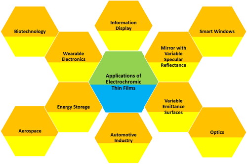
6.1. Information display
The electrochromic devices are studied since the discovery of information displays [Citation281]. The reflectance mode is usually the working mode for these devices. However, the EC display is made to function in either reflectance or transmissive ways. The EC display is used in crowded places such as railway stations, traffic direction boards, airports etc., where people are walking; and thus, can be simply observed from any angle. Efforts are also underway to apply in digital watch and television. The principal inadequacies are with switching time and need for high color reliability or a big amount of switching cycles that need to be addressed. Electrofluorochromism enhances the potential uses of EC displays in low-light environments by improving the emission mode. Simultaneously, the utilization of both electrical and light stimulation (namely, the excitation beam) in the information display amplifies its capability for anti-counterfeiting, encrypting it and diagnostic applications such as biosensors. Currently, two basic display prototypes exist: segmented and pixel displays, which are distinguished by their distinct operational principles as well as information capacity. Suitable EC displays have higher efficiency demands than other EC applications such as smart windows and antiglare rearview mirrors. Faster response speed for quick information display and switching, better stability and resilience to prolong their lifespan, and more optical contrast to ensure a pleasant reading experience are among these benefits. Nowadays, via extensive investigation on EC materials, a wide range of bright and rich colors have been achieved. This serves as the basis for the development of multicolored EC pixel displays. The color adjustment of organic EC materials mostly relies on structural transformation [Citation282,Citation283]. For instance, the viologens colors in the reduced states are significantly influenced by the associated functional group, conjugation degree, and even counter anions [Citation284,Citation285]. Further, the lateral chain functionalization technique is extensively employed to achieve the color adaptation of conjugated polymers [Citation45,Citation286]. In addition, structural color is typically employed to expand the range of colors available in the EC spectrum [Citation287,Citation288].
6.2. Mirror with variable specular reflectance
Important applications of ECDs are the EC mirrors function in a reflectance mode. When a color is made which is optically absorbing over the shiny surface, its reflecting intensity is decreased [Citation10]. To keep a gentle reflection in the darkened state, here total opacity is to be escaped. The most important applications of self-darkening EC rearview mirror are normally accessible for vehicles such as cars. During the daytime, the part of the mirror that is back-reflecting, results in the EC constituent in a bleached state, thereby adjusting the rearview mirror. During night, the mirror is aligned in a way that the headlights of the cars behind only attack a photosensitive sensor on the facade surface of the glass mirror. Consequently, it counters the light resulting from vehicles hence enhancing driver’s ease. This instrument requests to bright to variation about 104–105 cycles at least at a converting time of fewer than 5s, without visible degradation [Citation289].
6.3. Smart windows
The EC windows are one of the most significant uses of ECDs, which are obtainable in the market. It is new technological progress also known as ‘Smart Windows’ which provides comfort by spontaneously controlling the extent of light and solar energy in structures [Citation277,Citation290]. Skylights or architectural glazing also using it to regulate the solar heat arrival and to minimize energy consumption in summer for air conditioning and heating in winter [Citation291,Citation292]. Additionally, in order to avoid dazzling, it is also used in automobiles, trains, and airplanes. Such a device must have switched time within few seconds or maximum up to few minutes and a high transmittance variation and period of 20 years at least. Majority of controlling techniques for flexible EC windows described in the literature rely on fundamental rule-based control methods, that consider factors such as illumination temperature, gaze, and irradiance [Citation291]. For instance, Cannavale et al. [Citation293] conducted a comparison of the influences of all three control techniques (illumination, gaze, and irradiance based) on the energy savings and day lights of EC Windows. The findings confirmed that the illumination-based control technique offers the best balance between achieving maximum energy savings throughout the year and effectively utilizing day lighting. Platzer discovered that the most minimal initial energy utilization was achieved by switching based on room temperature [Citation294]. Tavares et al. [Citation295] performed a study to examine how various environmental parameters affect the energy supply of EC Windows. They demonstrated that optimizing the optical features of EC Windows in response to incident radiation yields the most favorable outcomes in a Mediterranean climate.
6.4. Variable emittance surfaces
EC materials have the ability to alter their optical features when an electric voltage is applied. This change occurs due to the electrochemical redox reactions, resulting in devices that can control the transmission, reflection, absorption, and emittance [Citation296]. These are specially planned WO3 film with good quality crystallinity. The surface whose thermal emittance is high is made by infrared reflecting or absorbing during intercalation/deintercalation ions [Citation279]. For instance, the emissivity of WO3 EC thin films exhibited substantial variation, reaching values as high as 78% and 49% in the mid-wave (3‒5µm) and long-wave (8‒12µm) bands, respectively [Citation297]. The phenomenon of EC results in the reversible change of color by electrochemical processes, which entail the simultaneous injection and extraction of both ions and electrons. During the applied voltage, the EC layer undergoes a color change that is directly correlated with the voltage. This color change is facilitated by the injection or ejection of ions [Citation298,Citation299]. The EC can alter the emissivity properties of materials, allowing us to choose the suitable voltage to regulate infrared radiation precisely and achieve smart thermal control. Radiation modulation can be achieved in the near infrared, thermal infrared, and microwave ranges [Citation300,Citation301]. The EC variable emissivity materials have been extensively explored for their utilization in the visible and near infrared (IR) spectrum bands. These materials include PANI, WO3, polythiophene, and its derivatives [Citation302–304].
6.5. Optics
The EC materials can be integrated into lenses for eyeglasses or camera filters, enabling users to change the color of the lenses according to their desires or the surrounding conditions [Citation305]. The EC thin films have the ability to function as adjustable optical filters in scientific instruments [Citation306]. In fluorescence microscopy, filters can be calibrated to selectively allow certain wavelengths of light to pass through for the purpose of imaging. The EC filters have the capability to regulate the degree and intensity of light that enters the camera, making them suitable for photography purposes. Photographers have the ability to adjust the filter parameters in a dynamic manner in order to obtain specific implications, without the need to manually change the filters [Citation307]. The EC thin films can also be applied on optical lenses, such as those employed in telescopes, to regulate the intensity of sunlight that enters the system. This is particularly advantageous in solar observations or imaging, where precise light adjustment is essential [Citation308].
6.6. Automotive industry
The EC thin films have become increasingly popular in the automobile sector, playing a crucial role in enhancing comfort, safety, and energy efficiency [Citation309]. Rearview mirrors feature EC technology, enabling drivers to adjust the mirror’s tint in order to minimize glare caused by headlights from vehicles behind them. This improves the ability to see clearly and decreases the discomfort in the eyes while driving at night. Further, the EC technology can also be incorporated into rearview camera displays, which allows for the automatic change of brightness and contrast according to the surrounding lighting conditions, assuring the best possible visibility for the drivers [Citation219,Citation310]. Furthermore, the EC thin films can be used in auto-dimming headlights to automatically change the light beam intensity and direction according to the presence of oncoming traffic and the surrounding lighting conditions. This improves safety by minimizing glare for both the driver and other individuals on the road. In addition, a number of luxury vehicles integrate EC technology into their sunroofs and windows. This feature enables passengers to regulate the intensity of sunlight that enters the car, so enhancing comfort and minimizing the need for conventional sunshades [Citation307].
6.7. Energy storage
Electrochromic thin-film technology is used to build electrochromic batteries that can store and release energy on demand in energy storage applications. Electrochromic batteries offer a high energy density and can be repeatedly charged and discharged. Transition metal oxides, MXenes, conjugated polymers, Metal-organic frameworks, and hybrid system have been investigated for the purpose of creating single EC batteries, with particular emphasis on hybrid systems [Citation311–313]. Nevertheless, there are several unresolved challenges concerning the precise capability, stability, coloration efficiency, and response time. Viologen, an organic substance with electrochromic properties, has been currently utilized in EC batteries. Incorporating chalcogens (Se, Te, and S) into the moieties of viologen remarkably enhances the capacity and cyclic stability of batteries. This technique was also utilized for the construction of flexible organic EC batteries, thereby introducing a revolutionary approach for energy storage using viologen molecules [Citation314]. Recently, Wang et al. [Citation315] investigated the use of a metal electrode and an anion exchange membrane to create a Zn–viologen hybrid battery. The system also possesses an additional feature known as the EC mirror state. Electrodeposition of Zn atoms onto the Zn-ITO electrode is facilitated by the viologen reduction (V2+ to V˙+) at cathode. During the charging process of the battery, it is possible that the conversion of electrical energy into chemical energy leads to the creation of a mirror state. The specific capacity was determined to be 65.0 mA h g−1, indicating the estimated stored energy. Furthermore, the same system exhibited a prolonged open-circuit memory effect, achieving a notable optical reflectance (i.e. 84.9%).
6.8. Aerospace
The EC thin films have several uses in the aerospace sector, aiding in the improvement of airplanes and spacecraft by providing increased functionality, energy efficiency, and enhanced safety [Citation316]. The EC windows provide the capability to adjust the darkness of aircraft windows in response to changes in external light conditions. This assists in lowering gaze, improving vision for pilots, and increasing passenger comfort. For example, PPG Aerospace has created electrochromic window systems specifically designed for use in both commercial and military aircraft. EC materials can be incorporated into cockpit displays to enable tailored color or transparency. This feature can be utilized to enhance visibility in varying lighting situations or minimize reflections on instrument panels, hence enhancing pilot performance [Citation317]. Further, EC coatings can be used on airplane cabin surfaces, such as walls and ceilings, to regulate the intensity of sunlight entering the cabin. By regulating the transparency of these coatings, it is feasible to optimize the natural lighting, minimizing the need of artificial lighting, and enhancing the energy efficiency inside the cabin [Citation318,Citation319]. In addition, EC thin films can be utilized on the outside surfaces of spacecraft to manage the heat loads. The EC thin films play a significant role in thermal control for spacecraft operating in severe climates by regulating the reflectance or emissivity of the surfaces according to the thermal conditions [Citation320].
6.9. Wearable electronics
Wearable technology employs EC thin-film technology to fashion smart glasses and other devices that can change color or transparency in response to external stimuli. This technology can be used to produce fashion accessories that change the appearance depending on the wearer’s choices or the environment conditions [Citation321]. For instance, Sinha et al. [Citation322] developed an electrochromic fabric display using a synthetic leather substrate made of poly(ethylene terephthalate). The electrochromic fabric demonstrated a switching speed of approximately 30 s while transitioning from red to blue colors. Additionally, these displays had a desirable fabric quality suitable for wearable purposes. Likewise, Yan et al. [Citation321] utilized Ag nanowires networks incorporated inside a polydimethylsiloxane (PDMS) elastomer matrix as flexible conductors with the stretching ability. The PDMS conductors demonstrated exceptional flexibility, enabling for a 50% strain, while also exhibiting favorable electrochromic performance with coloration occurring in 1 s and bleaching in 4 s.
6.10. Biotechnology
In the realm of biotechnology, EC thin films are utilized in diverse fashions to improve or facilitate numerous processes. The EC thin films can be included into biosensors to detect the presence of particular biomolecules. Thin films have the ability to change their color when target molecules adhere to them, thus producing a visual or electronic signal [Citation299]. Transparent substrates coated with EC thin films can be utilized for real-time monitoring of cell cultures and variations in the coloration of the film may suggest fluctuations in cell viability, growth, or metabolic activity. Further, EC thin films can be integrated into drug delivery devices to visually signify the drugs release and variation in coloration can be initiated by the discharge of particular chemicals from the drugs carriers [Citation323,Citation324]. Furthermore, EC thin films incorporated into cell culture substrates can be utilized to regulate the intensity of light exposure to cells. Researchers can regulate cellular responses with precision and control by using light to stimulate cells [Citation320]. In addition, EC thin films can be integrated into wearable devices for the purpose of monitoring physiological parameters. For example, a relatively advanced bandage with an electrochromic indicator might visually display information regarding the status of wound healing [Citation325].
Based on the considerable literature, it is possible to state that there is a close relationship between the structure and performance of films. The link between film structure and performance is an important component in establishing the film’s functional properties for a certain application. Film structures such as thickness, shape, and composition influence optical and electrochemical properties, which in turn influence the film performance. For example, the shape of a film can influences its electrochemical features such as capacity, stability, and response time. A porous shape can improve ion diffusion and the electrochemical performance of a thin film. A dense morphology, on the other hand, can improve the mechanical properties of the film while also limiting/restricting ion diffusion and lowering electrochemical performance. Similarly, the chemical composition of the film can alter optical features such as transmittance and coloring efficiency. The optical characteristics and coloration efficiency of the film can be affected by the EC material used and the stoichiometry of the film. The optical properties of a film can also be affected by its thickness, with thinner films often exhibiting higher transmittance and faster response times. Yet, increasing the thickness of the film reduces its mechanical strength. As a result, knowing the relationship between film structure and performance is critical for designing and optimizing EC thin films for specific applications. The optical and electrochemical properties of films can be tailored to suit specific application needs by adjusting film shape, composition, and thickness [Citation8,Citation326]. Several electrochromic thin film materials, their coloration efficiency, coloration time, bleaching time, and optical modulation are provided in .
Table 2. Electrochromic thin films devices, their coloration efficiency, coloration and bleaching time, and optical modulation.
7. Conclusions, challenges and future perspectives
In conclusion, in this review we have discussed, various fabrication methods of EC thin films, their functionalization and applications. The ability to change colour or transparency in response to applied voltage leads to products such as energy efficient smart windows, advanced energy storage, wearable electronics, display technology, anti-glare coatings, smart mirrors, Internet of Things (IoT) devices and environmental sensing. EC thin films are transforming the industry by providing dynamic and flexible functionality with a variety of features. These offer the benefits such as energy savings, enhanced user experience, greater privacy control, and integration with emerging technologies such as the IoT.
Conversely, further research and improvement are required to optimize the performance, durability and cost-effectiveness of EC thin films. Challenges such as long-term stability and durability, response time, colour options, colour range and stability, power consumption, and scalability must be addressed to ensure comprehensive approval. With current advances in materials science and engineering, they appear to be more organized, more durable, and commercially sustainable. Addressing these challenges requires continued research and development efforts, collaboration between academia and industry, and improvements in materials science, manufacturing methods, and equipment’s. These footprints will pave the way for fruitful applications of EC thin films in a variety of fields and maximize their potential.
Constant research and innovation in this field can lead to innovative applications impacting energy savings, aesthetics and functionality in a variety of fields. In addition, various synthesis methods of EC thin films are also limited, thus different methods had to be used to synthesize different EC thin films. Moreover, to improve the overall potential applications of this class of materials, it is suggested that the functionalization of EC films using various nanomaterials comprised of binary, ternary, and quaternary composites with thin polymer films has not been well covered in the literature. So, there is a need to address this area of innovative material.
Finally, the future vision of EC thin films is hopeful and has the potential to reshape industries and contribute to a more sustainable and technologically innovative future. Therefore, continued research and development in this area may lead to the development of devices that are more efficient, durable, highly scalable and have a wide range of practical applications.
Author contributions
Conceptualization, M. H., A. K. and M. B.; writing—original draft preparation, M. Y., M. A. K. K. and S. B.; writing—review and editing, M. H., M. U., N. A. K. and A. A. A. P.; supervision, M. H., A. K., R. A. A. and M. B. All authors have read and approved the submission of this manuscript.
Acknowledgments
The authors are grateful to Abdul Wali Khan University Mardan, Pakistan, and Prince Sultan University (PSU), Riyadh, Saudi Arabia for their overall support during this work. The authors would like to thank PSU for paying the APC.
Disclosure statement
No potential conflict of interest was reported by the author(s).
Additional information
Notes on contributors

Abbas Khan
Abbas Khan received his Ph.D. degree in Physical Chemistry from Quaid-I-Azam University, Islamabad, Pakistan, in 2010. After completion of PhD he first joined NCE in Physical Chemistry UOP and then the Department of Chemistry, Abdul Wali Khan University Mardan Pakistan as an Assistant Professor in 2011. In 2013, he worked as a Postdoc Research Fellow at the Universiti Sains Malaysia (USM), Malaysia. Currently, he is working as a Full Professor of Physical Chemistry at the same University. He is the author/co-author of more than 133 international peer-reviewed publications with citations over 2800 (h-index 26). In addition, Dr. Khan has also published several book chapters, conference proceedings. His research interests include Polymer Science, Colloidal Science; Surfactants, and Functional Materials Chemistry.

Mohamed Bououdina
Mohamed Bououdina received his PhD degree in Physics from Grenoble Alpes University, France. Currently, he is the Leader of the Energy, Water, and Environment Lab at Prince Sultan University Riyadh Saudi Arabia. He has over 25 years of teaching and research experience. He has a broad background and extensive expertise in Physics, Materials Science and Engineering, Nanotechnology, and Energy, specifically in Materials fabrication, analytical/spectroscopic characterizations, and properties/performance for cutting-edge technologies alongside computational modelling. He published over 500 papers in ISI journals with a H-index of 59, over 20 book chapters, and 2 indexed books.

Muhammad Usman
Muhammad Usman received a Ph.D. degree from the Chinese Academy of Sciences in 2014. He has completed two postdoctoral fellowships from Tsinghua University, China, and UC-Berkeley Global Science Institute node King Fahd University of Petroleum and Minerals (KFUPM). Since Sept 2018, he has been working as a Research Scientist (Assistant Professor) in the Interdisciplinary Research Center for Hydrogen and Energy Storage (previously known as the Center of Excellence in Nanotechnology, or CENT), at KFUPM, Saudi Arabia. His research activities are aimed at the utilization of zeolites and MOFs for CO2 capture, separation, and conversion. He holds several US patents and has published more than 80 publications in peer-reviewed international journals, in addition to several book chapters, conference proceedings/presentations.

Muhammad Humayun
Muhammad Humayun earned his Ph.D. in Physical Chemistry from Heilongjiang University China in 2017 and received Distinguished International Ph.D. Scholar award from Chinese Government. From Aug 2017 to Feb 2023, he worked as a Postdoc at Wuhan National Laboratory for Optoelectronics, Huazhong University of Science and Technology China. Currently, he is working as a Researcher (Assistant Professor) at the Energy, Water and Environment Lab, College of Humanities and Sciences, Prince Sultan University Riyadh Saudi Arabia. He has more than 120 publications with citations over 4980 (H-index 39). He has been included in Stanford University’s list of World’s top 2% scientists in 2023. His research interests include the design of functional nanomaterials for energy and environmental applications.
References
- Saqib N, Radulescu M, Usman M, et al. Environmental technology, economic complexity, renewable electricity, environmental taxes and CO2 emissions: implications for low-carbon future in G-10 bloc. Heliyon. 2023;9(6):e16457. doi: 10.1016/j.heliyon.2023.e16457.
- Saqib N, Usman M, Mahmood H, et al. The moderating role of technological innovation and renewable energy on CO2 emission in O.E.C.D. countries: evidence from panel quantile regression approach. Econ Res Ekon. 2023;36(3):2168720. doi: 10.1080/1331677X.2023.2168720.
- Uddin I, Usman M, Saqib N, et al. Correction to: the impact of geopolitical risk, governance, technological innovations, energy use, and foreign direct investment on CO2 emissions in the BRICS region. Environ Sci Pollut Res Int. 2023;30(31):77957–77957. doi: 10.1007/s11356-023-28076-w.
- Kim KH, Jeong SJ, Koo BR, et al. Surface amending effect of N-doped carbon-embedded NiO films for multirole electrochromic energy-storage devices. Appl Surf Sci. 2021;537:147902. doi: 10.1016/j.apsusc.2020.147902.
- Kim KH, Koo BR, Ahn HJ. Effects of Sb-doped SnO2–WO3 nanocomposite on electrochromic performance. Ceram Int. 2019;45(13):15990–15995. doi: 10.1016/j.ceramint.2019.05.109.
- Lusis A, Kleperis J, Pentjušs E. Model of electrochromic and related phenomena in tungsten oxide thin films. J Solid State Electrochem. 2003;7(2):106–112. doi: 10.1007/s10008-002-0315-2.
- Niklasson GA, Granqvist CG. Electrochromics for smart windows: thin films of tungsten oxide and nickel oxide, and devices based on these. J Mater Chem. 2007;17(2):127–156. doi: 10.1039/B612174H.
- Somani PR, Radhakrishnan S. Electrochromic materials and devices: present and future. Mater Chem Phys. 2003;77(1):117–133. doi: 10.1016/S0254-0584(01)00575-2.
- Yang P, Sun P, Mai W. Electrochromic energy storage devices. Mater Today. 2016;19(7):394–402. doi: 10.1016/j.mattod.2015.11.007.
- Buch VR, Chawla AK, Rawal SK. Review on electrochromic property for WO3 thin films using different deposition techniques. Mater Today. 2016;3(6):1429–1437. doi: 10.1016/j.matpr.2016.04.025.
- Granqvist CG, Arvizu MA, Pehlivan IB, et al. Electrochromic materials and devices for energy efficiency and human comfort in buildings: a critical review. Electrochim Acta. 2018;259:1170–1182. doi: 10.1016/j.electacta.2017.11.169.
- Granqvist CG. Handbook of inorganic electrochromic materials. Amsterdam: Elsevier B.V.; 1995.
- Sibilio S, Rosato A, Scorpio M, et al. A review of electrochromic windows for residential applications. IJHT. 2016;34(S2):S481–S488. doi: 10.18280/ijht.34S241.
- Patel K, Bhatt G, Ray J, et al. All-inorganic solid-state electrochromic devices: a review. J Solid State Electrochem. 2017;21(2):337–347. doi: 10.1007/s10008-016-3408-z.
- Monk PM, Ali T, Partridge RD. The effect of doping electrochromic molybdenum oxide with other metal oxides: correlation of optical and kinetic properties. Solid State Ion. 1995;80(1–2):75–85. doi: 10.1016/0167-2738(95)00130-X.
- Chang I, Kmetz A, Von Willisen F. Nonemissive electrooptic displays. New York: Plenum; 1976.
- Rosseinsky DR, Mortimer RJ. Electrochromic systems and the prospects for devices. Adv Mater. 2001;13(11):783–793. doi: 10.1002/1521-4095(200106)13:11%3C783::AID-ADMA783%3E3.0.CO;2-D.
- Granqvist CG. Electrochromic tungsten oxide films: review of progress. Sol Energy Mater Sol Cells. 2000;60(3):201–262. doi: 10.1016/S0927-0248(99)00088-4.
- Granqvist C. Progress in electrochromics: tungsten oxide revisited. Electrochim Acta. 1999;44(18):3005–3015. doi: 10.1016/s0013-4686(99)00016-x.
- Mortimer RJ. Organic electrochromic materials. Electrochim Acta. 1999;44(18):2971–2981. doi: 10.1016/S0013-4686%2899%2900046-8.
- Mortimer RJ. Electrochromic materials. Chem Soc Rev. 1997;26(3):147–156. doi: 10.1039/cs9972600147.
- Granqvist CG, Avendaño E, Azens A. Electrochromic coatings and devices: survey of some recent advances. Thin Solid Films. 2003;442(1–2):201–211. doi: 10.1016/S0040-6090(03)00983-0.
- Granqvist CG. Electrochromic metal oxides: an introduction to materials and devices. In: Mortimer RJ, Rosseinsky DR, Monk PMS, editors. Electrochromic materials and devices. Germany: Wiley‐VCH Verlag GmbH & Co. KGaA; 2013. p. 1–40. doi: 10.1002/9783527679850.ch1.
- Ohno H, Yamazaki H. Preparation and characteristics of all solid-state electrochromic display with cation-conductive polymer electrolytes. Solid State Ionics. 1993;59(3–4):217–222. doi: 10.1016/0167-2738(93)90053-6.
- Granqvist CG. Electrochromic devices. J Eur Ceram. 2005;25(12):2907–2912. doi: 10.1016/j.jeurceramsoc.2005.03.162.
- Corr D, Bach U, Fay D, et al. Coloured electrochromic paper quality displays based on modified mesoporous electrodes. Solid State Ionics. 2003;165(1–4):315–321. doi: 10.1016/j.ssi.2003.08.054.
- Lin SY, Chen YC, Wang CM, et al. Study of MoO3–NiO complementary electrochromic devices using a gel polymer electrolyte. Solid State Ionics. 2012;212:81–87. doi: 10.1016/j.ssi.2012.02.005.
- Riza MA, Ibrahim MA, Ahamefula UC, et al. Prospects and challenges of perovskite type transparent conductive oxides in photovoltaic applications. Part I–material developments. Sol Energy. 2016;137:371–378. doi: 10.1016/j.solener.2016.08.042.
- Bright C. Review of transparent conductive oxides (TCO). In: Mattox DM, Mattox VH, editors. 50 Years of vacuum coating technology and the growth of the society of vacuum coaters. Tuscon (AZ): 3M Company; 2007. p. 38–45.
- Chen Y, Wang Y, Sun P, et al. Nickel oxide nanoflake-based bifunctional glass electrodes with superior cyclic stability for energy storage and electrochromic applications. J Mater Chem A. 2015;3(41):20614–20618. doi: 10.1039/C5TA04011F.
- Bisht H, Eun HT, Mehrtens A, et al. Comparison of spray pyrolyzed FTO, ATO and ITO coatings for flat and bent glass substrates. Thin Solid Films. 1999;351(1–2):109–114. doi: 10.1016/S0040-6090(99)00254-0.
- Kim TH, Park SH, Kim DH, et al. Roll-to-roll sputtered ITO/Ag/ITO multilayers for highly transparent and flexible electrochromic applications. Sol Energy Mater Sol Cells. 2017;160:203–210. doi: 10.1016/j.solmat.2016.10.033.
- Akanda MR, Osman AM, Nazal MK, et al. Review recent advancements in the utilization of indium tin oxide (ITO) in electroanalysis without surface modification. J Electrochem Soc. 2020;167(3):037534. doi: 10.1149/1945-7111/ab64bd.
- Way A, Luke J, Evans AD, et al. Fluorine doped tin oxide as an alternative of indium tin oxide for bottom electrode of semi-transparent organic photovoltaic devices. AIP Adv. 2019;9(8):085220. doi: 10.1063/1.5104333.
- Kawashima T, Ezure T, Okada K, et al. FTO/ITO double-layered transparent conductive oxide for dye-sensitized solar cells. J Photochem Photobiol A. 2004;164(1–3):199–202. doi: 10.1016/j.jphotochem.2003.12.028.
- Deb S. A novel electrophotographic system. Appl Opt. 1969;8(S1):192–195. doi: 10.1364/AO.8.000192.
- Deb S. Optical and photoelectric properties and colour centres in thin films of tungsten oxide. Philos Mag. 1973;27(4):801–822. doi: 10.1080/14786437308227562.
- Giglia R. Features of an electrochromic display device. SID Symp Digest. 1975;6:52.
- Chang I, Gilbert B, Sun T. Electrochemichromic systems for display applications. J Electrochem Soc. 1975;122(7):955–962. doi: 10.1149/1.2134377.
- Goodman L. Passive liquid displays: liquid crystals, electrophoretics and electrochromics. IEEE Trans Consumer Electron. 1975;CE-21(3):247–259. doi: 10.1109/TCE.1975.266744.
- Faughnan BW, Crandall RS, Heyman PM. Electrochromism in WO3 amorphous films. RCA Rev. 1975;36(1):177–197.
- Lorteije J. A survey of drive methods for gas discharge, light emitting diode, liquid crystal and electrochromic displays. 1975;28(6):196–200.
- Mikhailov D, Yefanova V, Mikhailova A. Solid-state electrochromic indicator. Russ J Electrochem. 2011;47(8):871–876. doi: 10.1134/S1023193511080106.
- Beaujuge PM, Reynolds JR. Color control in π-conjugated organic polymers for use in electrochromic devices. Chem Rev. 2010;110(1):268–320. doi: 10.1021/cr900129a.
- Dyer AL, Thompson EJ, Reynolds JR. Completing the color palette with spray-processable polymer electrochromics. ACS Appl Mater Interfaces. 2011;3(6):1787–1795. doi: 10.1021/am200040p.
- Jang JE, Cha SN, Lee JM, et al. Multiple color reflection in a single unit cell using double-layer electrochromic reaction. Opt Lett. 2012;37(2):235–237. doi: 10.1364/OL.37.000235.
- Jensen J, Dam HF, Reynolds JR, et al. Manufacture and demonstration of organic photovoltaic‐powered electrochromic displays using roll coating methods and printable electrolytes. J Polym Sci B Polym Phys. 2012;50(8):536–545. doi: 10.1002/polb.23038.
- Tehrani P, Hennerdal LO, Dyer AL, et al. Improving the contrast of all-printed electrochromic polymer on paper displays. J Mater Chem. 2009;19(13):1799–1802. doi: 10.1039/b820677e.
- Tehrani P, Engquist I, Robinson ND, et al. Printable organic electrochemical circuit to record time–temperature history. Electrochim Acta. 2010;55(23):7061–7066. doi: 10.1016/j.electacta.2010.06.073.
- Said E, Andersson P, Engquist I, et al. Electrochromic display cells driven by an electrolyte-gated organic field-effect transistor. Org Electronics. 2009;10(6):1195–1199. doi: 10.1016/j.orgel.2009.06.008.
- Liu H, Crooks RM. Paper-based electrochemical sensing platform with integral battery and electrochromic read-out. Anal Chem. 2012;84(5):2528–2532. doi: 10.1021/ac203457h.
- Baloukas B, Lamarre JM, Martinu L. Active metameric security devices using an electrochromic material. Appl Opt. 2011;50(9):C41–C49. doi: 10.1364/AO.50.000C41.
- Baloukas B, Martinu L. WO3/SiO2 composite optical films for the fabrication of electrochromic interference filters. Appl Opt. 2012;51(16):3346–3356. doi: 10.1364/AO.51.003346.
- Piegari P, Flory F. Optical thin films and coatings: from materials to applications. Cambridge: Woodhead Publishing; 2018.
- Shin H, Kim Y, Bhuvana T, et al. Color combination of conductive polymers for black electrochromism. ACS Appl Mater Interfaces. 2012;4(1):185–191. doi: 10.1021/am201229k.
- Ukoba KO, Eloka-Eboka AC, Inambao FL. Review of nanostructured NiO thin film deposition using the spray pyrolysis technique. Renew Sust Energ Rev. 2018;82:2900–2915. doi: 10.1016/j.rser.2017.10.041.
- Morosanu CE. Thin films by chemical vapour deposition. In: Volume 7 of Thin films science and technology. Amsterdam: Elsevier Science; 1990.
- Leskelä M, Ritala M. Atomic layer deposition (ALD): from precursors to thin film structures. Thin Solid Films. 2002;409(1):138–146. doi: 10.1016/S0040-6090(02)00117-7.
- Yang TS, Cho W, Kim M, et al. Atomic layer deposition of nickel oxide films using Ni (dmamp) 2 and water. J Vac Sci Technol. 2005;23(4):1238–1243. doi: 10.1116/1.1875172.
- Rozati S, Akesteh S. Characterization of ZnO:Al thin films obtained by spray pyrolysis technique. Mater Charact. 2007;58(4):319–322. doi: 10.1016/j.matchar.2006.05.012.
- Sta I, Jlassi M, Hajji M, et al. Structural, optical and electrical properties of undoped and Li-doped NiO thin films prepared by sol–gel spin coating method. Thin Solid Films. 2014;555:131–137. doi: 10.1016/j.tsf.2013.10.137.
- Xu X, Xia C, Huang S, et al. YSZ thin films deposited by spin-coating for IT-SOFCs. Ceram Int. 2005;31(8):1061–1064. doi: 10.1016/j.ceramint.2004.11.005.
- Brinker C, Frye G, Hurd A, et al. Fundamentals of sol-gel dip coating. Thin Solid Films. 1991;201(1):97–108. doi: 10.1016/0040-6090(91)90158-T.
- Wang H, Wang Y, Wang X. Pulsed laser deposition of the porous nickel oxide thin film at room temperature for high-rate pseudocapacitive energy storage. Electrochem Commun. 2012;18:92–95. doi: 10.1016/j.elecom.2012.02.023.
- Mahan JE. Physical vapor deposition of thin films. New York: Wiley; 2000.
- Herman MA, Sitter H. Molecular beam epitaxy: fundamentals and current status. Berlin, Heidelberg: Springer; 2012.
- Zhao Y, Wang H, Wu C, et al. Structures, electrical and optical properties of nickel oxide films by radio frequency magnetron sputtering. Vacc. 2014;103:14–16. doi: 10.1016/j.vacuum.2013.11.009.
- Xia X, Tu J, Zhang J, et al. Electrochromic properties of porous NiO thin films prepared by a chemical bath deposition. Sol Energy Mater Sol. 2008;92(6):628–633. doi: 10.1016/j.solmat.2008.01.009.
- Luyo C, Ionescu R, Reyes LF, et al. Gas sensing response of NiO nanoparticle films made by reactive gas deposition. Chem Sens. 2009;138(1):14–20. doi: 10.1016/j.snb.2008.11.057.
- Kalita PK, Sarma B, Das H. Structural characterization of vacuum evaporated ZnSe thin films. Bull Mater Sci. 2000;23(4):313–317. doi: 10.1007/BF02720089.
- Tanuševski A, Poelman D. Optical and photoconductive properties of SnS thin films prepared by electron beam evaporation. Sol Energy Mater Sol Cells. 2003;80(3):297–303. doi: 10.1016/j.solmat.2003.06.002.
- Lampert C, Omstead T, Yu P. Chemical and optical properties of electrochromic nickel oxide films. Sol Energy Mater. 1986;14(3–5):161–174. doi: 10.1016/0165-1633(86)90043-2.
- Liang F, Yang J, Zhao Y, et al. A review of thin film electrolytes fabricated by physical vapor deposition for solid oxide fuel cells. Int J Hydrog Energy. 2022;47(87):36926–36952. doi: 10.1016/j.ijhydene.2022.08.237.
- Rossnagel SM. Thin film deposition with physical vapor deposition and related technologies. J Vac Sci Technol A. 2003;21(5):S74–S87. doi: 10.1116/1.1600450.
- Sun L, Yuan G, Gao L, et al. Chemical vapour deposition. Nat Rev Methods Primers. 2021;1(1):5. doi: 10.1038/s43586-020-00005-y.
- Sequeda FO. Thin film deposition techniques in microelectronics. JOM. 1986;38(2):55–65. doi: 10.1007/BF03257928.
- Livage J, Ganguli D. Sol–gel electrochromic coatings and devices: a review. Sol Energy Mater Sol Cells. 2001;68(3–4):365–381. doi: 10.1016/S0927-0248(00)00369-X.
- Nishio K, Tsuchiya T. Electrochromic thin films prepared by sol-gel process. Sol Energy Mater Sol Cells. 2001;68(3–4):279–293. doi: 10.1016/S0927-0248(00)00362-7.
- Ezekoye BA, Offor PO, Ezekoye VA, et al. Chemical bath deposition technique of thin films: a review. Int J Recent Sci Res. 2012;2:589–592. doi: 10.15373/22778179/AUG2013/149.
- Tajima K, Kubota T, Jeong CY. Preparation of electrochromic thin films by humidity-controlled spin coating. Thin Solid Films. 2022;758:139412. doi: 10.1016/j.tsf.2022.139412.
- Park JH, Kang JS, Cha IY, et al. Preparation of WO3 thin film by successive dip coating for electrochromic and photoelectrochromic devices. Bulletin Korean Chem Soc. 2015;36(9):2213–2220. doi: 10.1002/bkcs.10424.
- Selvakumar N, Barshilia HC. Review of physical vapor deposited (PVD) spectrally selective coatings for mid-and high-temperature solar thermal applications. Sol Energy Mater Sol Cells. 2012;98:1–23. doi: 10.1016/j.solmat.2011.10.028.
- Lagaron J, Catalá R, Gavara R. Structural characteristics defining high barrier properties in polymeric materials. Mater Sci Technol. 2004;20(1):1–7. doi: 10.1179/026708304225010442.
- Kalss W, Reiter A, Derflinger V, et al. Modern coatings in high performance cutting applications. Int J Refract Hard Met. 2006;24(5):399–404. doi: 10.1016/j.ijrmhm.2005.11.005.
- Andreev AA, Gavrilko IV, Gavrilov AG, et al. Multilayer coatings of metal-cutting tools. United States Patents. US4554201A. 1985 Nov 19.
- Wang W, Chen W, Wang B, et al. Ultrathin ferroelectric films: growth, characterization physics and applications. Mater. 2014;7(9):6377–6485. doi: 10.3390/ma7096377.
- Chaffar Akkari F, Ben Jbara H, Abdelkader D, et al. Effect of angle deposition γ on the structural, optical and electrical properties of copper oxide zigzag (+γ, −γ) nanostructures elaborated by glancing angle deposition. Thin Solid Films. 2018;657:61–69. doi: 10.1016/j.tsf.2018.05.006.
- Pereira S, Gonçalves A, Correia N, et al. Electrochromic behavior of NiO thin films deposited by e-beam evaporation at room temperature. Sol Energy Mater Sol Cells. 2014;120:109–115. doi: 10.1016/j.solmat.2013.08.024.
- Sivakumar R, Shanthakumari K, Thayumanavan A, et al. Molybdenum oxide (MoO3) thin film based electrochromic cell characterisation in 0·1M LiClO4. PC electrolyte. Surf Eng. 2009;25(7):548–554. doi: 10.1179/174329408X282523.
- Duta L, Popescu A. C. Current status on pulsed laser deposition of coatings from animal-origin calcium phosphate sources. Coatings. 2019;9(5):335. doi: 10.3390/coatings9050335.
- Chrisey DB, Hubler GK. Pulsed laser deposition of thin films. New York: John Wiley & Sons; 1994.
- Eason R. Pulsed laser deposition of thin films: applications-led growth of functional materials. London: John Wiley & Sons; 2007.
- Rashidian Vaziri M, Hajiesmaeilbaigi F, Maleki M. Monte Carlo simulation of the subsurface growth mode during pulsed laser deposition. J Appl Phys. 2011;110(4):043304. doi: 10.1063/1.3624768.
- Cho AY, Arthur J. Molecular beam epitaxy. Prog Solid State Ch. 1975;10:157–191. doi: 10.1016/0079-6786(75)90005-9.
- Ohring M. Materials science of thin films: deposition and structure. San Diego (CA): Academic Press; 2002.
- Belmoubarik M, Nozaki T, Endo H, et al. Investigation of ZnO thin films deposited on ferromagnetic metallic buffer layer by molecular beam epitaxy toward realization of ZnO-based magnetic tunneling junctions. J Appl Phys. 2013;113(17):17C106. doi: 10.1063/1.4794875.
- Jabari‐Seresht R, Jahanshahi M, Rashidi A, et al. Fabrication and of non‐porous graphene by a unique spray pyrolysis method. Chem Eng Technol. 2013;36(9):1550–1558. doi: 10.1002/ceat.201300002.
- Udayakumar R, Khanaa V, Saravanan T. Synthesis and structural characterization of thin films of SnO2 prepared by spray pyrolysis technique. IJST. 2013;6(sp6):1–4. doi: 10.17485/ijst/2013/v6isp6.19.
- Cho M, Harada C, Suzuki H, et al. ZnO homoepitaxy. Superlattices Microstruct. 2005;38(4–6):349–363. doi: 10.1016/j.spmi.2005.08.022.
- Mattox DM. Atomistic film growth and some growth-related film properties. In: Handbook of physical vapor deposition (PVD) processing. 2nd ed. New York: William Andrew Publishing; 2010. p. 333–398.
- Schultz PG, Xiang XD, Goldwasser I, et al. Polymer arrays from the combinatorial synthesis of novel materials United States Patent, US 6,794,052 B2, 2004 Sep. 21.
- Seyfert U, Heisig U, Teschner G, et al. 40 Years of industrial magnetron sputtering in Europe. MRS Bull. 2015;26:182–189.
- Seshan K, Schepis D. Handbook of thin film deposition. New York: William Andrew Publishing; 2018.
- Seshan K. Handbook of thin film deposition processes and techniques. New York: William Andrew Publishing; 2001.
- Teixeira V, Cui H, Meng L, et al. Amorphous ITO thin films prepared by DC sputtering for electrochromic applications. Thin Solid Films. 2002;420-421:70–75. doi: 10.1016/S0040-6090(02)00656-9.
- Utsumi K, Iigusa H, Tokumaru R, et al. Study on In2O3–SnO2 transparent and conductive films prepared by dc sputtering using high density ceramic targets. Thin Solid Films. 2003;445(2):229–234. doi: 10.1016/S0040-6090(03)01167-2.
- Gómez A, Galeano A, Saldarriaga W, et al. Deposition of YBaCo4O7+ δ thin films on (001)-SrTiO3 substrates by dc sputtering. Vacc. 2015;119:7–14. doi: 10.1016/j.vacuum.2015.04.020.
- Cash JH, Jr, Cunningham JA. Rf sputtering method United States Patent, US3677924A, 1972 July 18.
- You T, Niwa O, Tomita M, et al. Characterization and electrochemical properties of highly dispersed copper oxide/hydroxide nanoparticles in graphite-like carbon films prepared by RF sputtering method. Electrochem Commun. 2002;4(5):468–471. doi: 10.1016/S1388-2481(02)00340-5.
- Torng C, Sivertsen JM, Judy JH, et al. Structure and bonding studies of the C: n thin films produced by RF sputtering method. J Mater Res. 1990;5(11):2490–2496. doi: 10.1557/JMR.1990.2490.
- Constantin DG, Apreutesei M, Arvinte RA, et al. Magnetron sputtering technique used for coatings deposition; technologies and applications. 7th International Conference on Materials Science and Engineering. 2011. p. 29–33.
- Christie DJ. Making magnetron sputtering work: modelling reactive sputtering dynamics, part 1. SVC Bulletin. 2014;127:24–27.
- Arnell RD, Kelly PJ. Recent advances in magnetron sputtering. Surf Coat Technol. 1999;112(1–3):170–176. doi: 10.1016/S0257-8972(98)00749-X.
- Musil J. Recent advances in magnetron sputtering technology. Surf Coat Technol. 1998;100–101:280–286. doi: 10.1016/S0257-8972(97)00633-6.
- Oluwatosin Abegunde O, Titilayo Akinlabi E, Philip Oladijo O, et al. Overview of thin film deposition techniques. AIMS Mater Sci. 2019;6(2):174–199. doi: 10.3934/matersci.2019.2.174.
- Jones AC, Hitchman ML. Chemical vapour deposition: precursors, processes and applications. Cambridge: Royal Society of Chemistry; 2009.
- Henley W, Sacks G. Deposition of electrochromic tungsten oxide thin films by plasma‐enhanced chemical vapor deposition. J Electrochem Soc. 1997;144(3):1045–1050. doi: 10.1149/1.1837528.
- Holonyak N, Jr, Kolbas R, Dupuis R, et al. Quantum-well heterostructure lasers. IEEE J Quant Electron. 1980;16(2):170–186.
- Duchemin J, Bonnet M, Koelsch F, et al. A new method for the growth of GaAs epilayer at low H2 pressure. J Cryst Growth. 1978;45:181–186. doi: 10.1016/0022-0248(78)90432-3.
- Kurishima K, Nakajima H, Yamahata S, et al. High‐performance Zn‐doped‐base InP/InGaAs double‐heterojunction bipolar transistors grown by metalorganic vapor phase epitaxy. Appl Phys Lett. 1994;64(9):1111–1113. doi: 10.1063/1.110844.
- Zvonkov NB, Zvonkov NB, Ershov AE, et al. Semiconductor lasers emitting at the 0.98 μm wavelength with radiation coupling-out through the substrate. Quantum Electron. 1998;28(7):605–607. doi: 10.1070/QE1998v028n07ABEH001287.
- Motoda T, Kato M, Kadoiwa K, et al. Multi-wafer growth of highly uniform and high-quality AlGaInP/GaInP structure using high-speed rotating disk metalorganic chemical vapor deposition. J cryst Growth. 1994;145(1–4):650–654. doi: 10.1016/0022-0248(94)91121-5.
- Shaheen SE, Radspinner R, Peyghambarian N, et al. Fabrication of bulk heterojunction plastic solar cells by screen printing. Appl Phys Lett. 2001;79(18):2996–2998. doi: 10.1063/1.1413501.
- Egawa T, Ishikawa H, Jimbo T, et al. Heteroepitaxial growth of III–V compound semiconductors for optoelectronic devices. Bull Mater Sci. 1999;22(3):363–367. doi: 10.1007/BF02749943.
- Toda A, Kawasumi T, Imanishi D, et al. Blue-green ZnCdSe light-emitting diodes grown by MOCVD. Electron Lett. 1995;31(3):235–237. doi: 10.1049/el:19950157.
- Sugiura S, Shigenaka K, Nakata F, et al. Misfit dislocation microstructure and kinetics of HgCdTe/CdZnTe under tensile and compressive stress. J Cryst Growth. 1994;145(1–4):547–551. doi: 10.1016/0022-0248(94)91105-3.
- Fujita S, Fujita S. Metalorganic vapor-phase epitaxy of p-type ZnSe and p/n junction diodes. J Cryst Growth. 1994;145(1–4):552–556. doi: 10.1016/0022-0248(94)91106-1.
- Anderson P, Erbil A, Nelson C, et al. A high-speed, rotating-disc metalorganic chemical vapor deposition system for the growth of (Hg, cd) Te and related alloys. J Cryst Growth. 1994;135(3–4):383–400. doi: 10.1016/0022-0248(94)90127-9.
- Pautrat JL, Monterrat E, Ulmer L, et al. Band gap engineering in II–VI based heterostructure. J Cryst Growth. 1992;117(1–4):454–459. doi: 10.1016/0022-0248(92)90791-G.
- Manasevit H, Simpson W. The use of metalorganics in the preparation of semiconductor materials: VI. Formation of IV–VI lead and tin salts. J Electrochem Soc. 1975;122(3):444–450. doi: 10.1149/1.2134233.
- Stamenković L. Chemical vapor deposition of coatings. Zaštita Materijala. 2007;48(2):25–48.
- Chandraboss V, Karthikeyan B, Kamalakkannan J, et al. Sol-Gel synthesis of TiO2/SiO2 and ZnO/SiO2 composite films and evaluation of their photocatalytic activity towards methyl green. J Nanopart. 2013;2013(7):1–7. doi: 10.1155/2013/507161.
- Peng YY, Hsieh TE, Hsu CH. White-light emitting ZnO-SiO2 nanocomposite thin films prepared by the target-attached sputtering method. Nanotechnol. 2005;17(1):174–180. doi: 10.1088/0957-4484/17/1/028.
- Alotaibi AM, Sathasivam S, Williamson BA, et al. Chemical vapor deposition of photocatalytically active pure brookite TiO2 thin films. Chem Mater. 2018;30(4):1353–1361. doi: 10.1021/acs.chemmater.7b04944.
- Lang J, Takahashi K, Kubo M, et al. Preparation of TiO2-CNT-Ag ternary composite film with enhanced photocatalytic activity via plasma-enhanced chemical vapor deposition. Catalyst. 2022;12(5):508. doi: 10.3390/catal12050508.
- de Oliveira AG, Nascimento JP, de Fátima Gorgulho H, et al. Electrochemical synthesis of TiO2/graphene oxide composite films for photocatalytic applications. J Alloys Compd. 2016;654:514–522. doi: 10.1016/j.jallcom.2015.09.110.
- Chien DT, Long PD, Van HP, et al. Nanocomposite thin film TiO2/CdS electrodes prepared by thermal evaporation process for photovoltaic applications. Comm in Phys. 2011;21(1):57–57. doi: 10.15625/0868-3166/21/1/95.
- Popescu-Pelin G, Ristoscu C, Duta L, et al. Fish bone derived bi-phasic calcium phosphate coatings fabricated by pulsed laser deposition for biomedical applications. Mar Drugs. 2020;18(12):623. doi: 10.3390/md18120623.
- Sugumaran S, Bellan CS, Nadimuthu M. Characterization of composite PVA–Al2O3 thin films prepared by dip coating method. Iran Polym J. 2015;24(1):63–74. doi: 10.1007/s13726-014-0300-5.
- Mohammad T, Alam F, Sadhanala A, et al. In sulfide (SnS) films deposited by an electric field-Assisted continuous spray pyrolysis technique with application as counter electrodes in Dye-Sensitized solar cells. ACS Omega. 2022;7(44):39690–39696. doi: 10.1021/acsomega.2c03454.
- LeClair P, Berera GP, Moodera J. Titanium nitride thin films obtained by a modified physical vapor deposition process. Thin Solid Films. 2000;376(1–2):9–15. doi: 10.1016/S0040-6090(00)01192-5.
- Sharma N, Hooda M, Sharma S. S. Synthesis and characterization of LPCVD polysilicon and silicon nitride thin films for MEMS applications. J Mater. 2014;2014:1–8. doi: 10.1155/2014/954618.
- Klobukowski ER, Tenhaeff WE, McCamy JW, et al. Atmospheric pressure chemical vapor deposition of high silica SiO2–TiO2 antireflective thin films for glass based solar panels. J Mater Chem C. 2013;1(39):6188–6190. doi: 10.1039/c3tc31465k.
- Lang J, Takahashi K, Kubo M, et al. Ag-doped TiO2 composite films prepared using Aerosol-Assisted, plasma-enhanced chemical vapor deposition. Catalyst. 2022;12(4):365. doi: 10.3390/catal12040365.
- Zhou L, Hoffmann RC, Zhao Z, et al. Chemical bath deposition of thin TiO2-anatase films for dielectric applications. Thin Solid Films. 2008;516(21):7661–7666. doi: 10.1016/j.tsf.2008.02.042.
- Ogirima M, Saida H, Suzuki M, et al. A multiwafer growth system for low pressure silicon epitaxy. J Electrochem Soc. 1978;125(11):1879–1881. doi: 10.1149/1.2131316.
- Kern W, Schnable GL. Low-pressure chemical vapor deposition for very large-scale integration processing—a review. IEEE Trans Electron Devices. 1979;26(4):647–657. doi: 10.1109/T-ED.1979.19473.
- Sharma N, Hooda M, Sharma KS. Synthesis and characterization of LPCVD polysilicon and silicon nitride thin films for MEMS applications. J Mater. 2014;2014:954618. doi: 10.1155/2014/954618.
- Venkatesan V. Low pressure chemical vapor deposition of silicon dioxide and phosphosilicate glass thin films [master’s thesis-1128]. New Jersey Institute of Technology; 1996. https://digitalcommons.njit.edu/theses/1128.
- Kern W, Rosler RS. Advances in deposition processes for passivation films. J Vacc Sci Technol. 1977;14(5):1082–1099. doi: 10.1116/1.569340.
- Baron M, Zelez J. Vacuum systems for plasma etching, plasma deposition; and low pressure CVD. Solid State Technol. 1978;21(12):61–82.
- Logar R, Herring R, Wauk M. C356–C356. Reduced pressure silicon epitaxy in a cylindrical geometry reactor. Pennington (NJ): Electrochemical Society Inc.; 1978.
- Ban VS. Novel reactor for high volume low-cost silicon epitaxy. J Cryst Growth. 1978;45:97–107. doi: 10.1016/0022-0248(78)90420-7.
- Drosos C, Vernardou D. Perspectives of energy materials grown by APCV. Sol Energy Mater Sol Cells. 2015;140:1–8. doi: 10.1016/j.solmat.2015.03.019.
- Hou X, Choy KL. Processing and applications of aerosol‐assisted chemical vapor deposition. Chem Vap Depos. 2006;12(10):583–596. doi: 10.1002/cvde.200600033.
- Lewkebandara TS, Winter CH. CVD routes to titanium disulfide films. Adv Mater. 1994;6(3):237–239. doi: 10.1002/adma.19940060313.
- Marchand P, Hassan IA, Parkin IP, et al. Aerosol-assisted delivery of precursors for chemical vapour deposition: expanding the scope of CVD for materials fabrication. Dalton Trans. 2013;42(26):9406–9422. doi: 10.1039/C3DT50607J.
- Price J, Wu SY. Plasma enhanced CVD, plasma enhanced CVD United States Patents, US4692343A, 1987 Sept. 08.
- Li Y, Mann D, Rolandi M, et al. Preferential growth of semiconducting single-walled carbon nanotubes by a plasma enhanced CVD method. Nano Lett. 2004;4(2):317–321. doi: 10.1021/nl035097c.
- Hozumi A, Takai O. Preparation of ultra water-repellent films by microwave plasma-enhanced CVD. Thin Solid Films. 1997;303(1-2):222–225. doi: 10.1016/S0040-6090(97)00076-X.
- Said B, Belgacem S, Dachraoui M, et al. Structural and optical properties of cdsub (1-y) znsub (y) S/CuPc bilayers: exhibition of a photovoltaic effect. Rev Phys Appl. 1986;21(7):407–415.
- Nair P, Nair M, Fernandez A, et al. Prospects of chemically deposited metal chalcogenide thin films for solar control application. J Phys D: appl Phys. 1989;22(6):829–836. doi: 10.1088/0022-3727/22/6/021.
- Suryanarayana C, Lakshmanan A, Subramanian V, et al. Preparation of thin film electrodes for electrochemical solar cells-chemical bath deposition. Bull Electrochem. 1986;2(1):57–58.
- Lokhande C. Chemical deposition of metal chalcogenide thin films. Mater Chem Phys. 1991;27(1):1–43. doi: 10.1016/0254-0584(91)90158-Q.
- Ibanez JG, Gomez F, Konik I, et al. Preparation of semiconducting materials in the laboratory, part 2: microscale chemical bath deposition of materials with band gap energies in the UV, VIS, and IR. J Chem Educ. 1997;74(10):1205. doi: 10.1021/ed074p1205.
- Lokhande CD, Ennaoui A, Patil PS, et al. Process and characterisation of chemical bath deposited manganese sulphide (MnS) thin films. Thin Solid Films. 1998;330(2):70–75. doi: 10.1016/S0040-6090(98)00500-8.
- Brinker CJ. Hydrolysis and condensation of silicates: effects on structure. J Non Cryst Solids. 1988;100(1–3):31–50. doi: 10.1016/0022-3093(88)90005-1.
- Fakoya MF, Shah SN. Emergence of nanotechnology in the oil and gas industry: emphasis on the application of silica nanoparticles. Petroleum. 2017;3(4):391–405. doi: 10.1016/j.petlm.2017.03.001.
- Glynn C, O'Dwyer C. Solution processable metal oxide thin film deposition and material growth for electronic and photonic devices. Adv Materials Inter. 2017;4(2):1600610. doi: 10.1002/admi.201600610.
- Bhuiyan M, Paranthaman M, Salama K. Solution-derived textured oxide thin films—a review. Supercond Sci Technol. 2006;19(2):R1–R21. doi: 10.1088/0953-2048/19/2/R01.
- Schneller T, Waser R, Kosec M, et al. Chemical solution deposition of functional oxide thin films. Vienna: Springer-Verlag Wien; 2013.
- Meyerhofer D. Characteristics of resist films produced by spinning. J Appl Phys. 1978;49(7):3993–3997. doi: 10.1063/1.325357.
- Birnie DP, Hau SK, Kamber DS, et al. Effect of ramping-up rate on film thickness for spin-on processing. J Mater Sci: Mater Electron. 2005;16(11–12):715–720. doi: 10.1007/s10854-005-4973-6.
- Emslie AG, Bonner FT, Peck LG. Flow of a viscous liquid on a rotating disk. J Appl Phys. 1958;29(5):858–862. doi: 10.1063/1.1723300.
- Rezende BA, dos Santos AJ, Câmara MA, et al. Characterization of ceramics coatings processed by sol-gel for cutting tools. Coat. 2019;9(11):755. doi: 10.3390/coatings9110755.
- Brinker C, Hurd A, Schunk P, et al. Review of sol-gel thin film formation. J Non-Cryst Solids. 1992;147–148:424–436. doi: 10.1016/S0022-3093(05)80653-2.
- Landau L, Levich B. Dragging of a liquid by a moving plate. In: Dynamics of curved fronts. Amsterdam: Elsevier, 1988. p. 141–153. doi: 10.1016/B978-0-08-092523-3.50016-2.
- Faustini M, Louis B, Albouy PA, et al. Preparation of sol − gel films by dip-coating in extreme conditions. J Phys Chem C. 2010;114(17):7637–7645. doi: 10.1021/jp9114755.
- Glynn C, Creedon D, Geaney H, et al. Inking precursor alterations to nanoscale structure and optical transparency in polymer assisted fast-rate dip-coating of vanadium oxide thin films. Sci Rep. 2015;5(1):11574. doi: 10.1038/srep11574.
- Nishida F, Dunn B, McKiernan J, et al. In-situ fluorescence imaging of sol-gel thin film deposition. J Sol-Gel Sci Technol. 1994;2(1–3):477–481. doi: 10.1007/BF00486294.
- Hurd AJ, Brinker CJ. Optical sol-gel coatings: ellipsometry of film formation. J Phys France. 1988;49(6):1017–1025. doi: 10.1051/jphys:019880049060101700.
- Krebs FC. Fabrication and processing of polymer solar cells: a review of printing and coating techniques. Sol Energy Mater Sol Cells. 2009;93(4):394–412. doi: 10.1016/j.solmat.2008.10.004.
- Abadi MHS, Hamidon MN, Shaari AH, et al. SnO2/Pt thin film laser ablated gas sensor array. Sensors. 2011;11(8):7724–7735. doi: 10.3390/s110807724.
- Moonen PF, Yakimets I, Huskens J. Fabrication of transistors on flexible substrates: from mass‐printing to high‐resolution alternative lithography strategies. Adv Mater. 2012;24(41):5526–5541. doi: 10.1002/adma.201202949.
- Menard E, Meitl MA, Sun Y, et al. Micro-and nanopatterning techniques for organic electronic and optoelectronic systems. Chem Rev. 2007;107(4):1117–1160. doi: 10.1021/cr050139y.
- Søndergaard R, Hösel M, Angmo D, et al. Roll-to-roll fabrication of polymer solar cells. Mater Today. 2012;15(1–2):36–49. doi: 10.1016/S1369-7021(12)70019-6.
- Xia C, Chen F, Liu M. Reduced-Temperature solid oxide fuel cells fabricated by screen printing. Electrochem Solid-State Lett. 2001;4(5):A52. DOI doi: 10.1149/1.1361158.
- Zielke D, Hübler AC, Hahn U, et al. Polymer-based organic field-effect transistor using offset printed source/drain structures. Appl Phys Lett. 2005;87(12):123508. doi: 10.1063/1.2056579.
- Guo Q, Ford GM, Yang WC, et al. Fabrication of 7.2% efficient CZTSSe solar cells using CZTS nanocrystals. J Am Chem Soc. 2010;132(49):17384–17386. doi: 10.1021/ja108427b.
- Gamota D R, Brazis P. Kalyanasundaram K, Zhang J, editors. Printed organic and molecular electronics. Boston, New York, London: Springer; 2004.
- Wen Y, Liu Y, Guo Y, et al. Experimental techniques for the fabrication and characterization of organic thin films for field-effect transistors. Chem Rev. 2011;111(5):3358–3406. doi: 10.1021/cr1001904.
- Nehru L, Umadevi M, Sanjeeviraja C. Studies on structural, optical and electrical properties of ZnO thin films prepared by the spray pyrolysis method. IJME. 2012;2(1):12–17. doi: 10.5923/j.ijme.20120201.03.
- Ilegbusi OJ, Khatami SN, Trakhtenberg LI. Spray pyrolysis deposition of single and mixed oxide thin films. MSA. 2017;08(02):153–169. v doi: 10.4236/msa.2017.82010.
- Messing GL, Zhang SC, Jayanthi GV. Ceramic powder synthesis by spray pyrolysis. J Am Ceram Soc. 1993;76(11):2707–2726. doi: 10.4236/msa.2017.82010.
- Seeber W, Abou-Helal M, Barth S, et al. Transparent semiconducting ZnO: al thin films prepared by spray pyrolysis. Mater Sci Semicond Process. 1999;2(1):45–55. doi: 10.1016/S1369-8001(99)00007-4.
- Okuya M, Shiozaki K, Horikawa N, et al. Porous TiO2 thin films prepared by spray pyrolysis deposition (SPD) technique and their application to UV sensors. Solid State Ionics. 2004;172(1–4):527–531. doi: 10.1016/j.ssi.2004.02.060.
- Chen C, Kelder E, Jak M, et al. Electrostatic spray deposition of thin layers of cathode materials for lithium battery. Solid State Ionics. 1996;86–88:1301–1306. doi: 10.1016/0167-2738(96)00305-0.
- Balkenende A, Bogaerts A, Scholtz J, et al. Thin MgO layers for effective hopping transport of electrons. Philips J Res. 1996;50(3–4):365–373. doi: 10.1016/S0165-5817(97)84680-3.
- Filipovic L, Selberherr S, Mutinati GC, et al. Modeling and analysis of spray pyrolysis deposited SnO2 films for gas sensors. In: Transactions on engineering technologies. Dordrecht: Springer Science + Business Media; 2014. p. 295–310.
- Perednis D, Gauckler LJ. Thin film deposition using spray pyrolysis. J Electroceram. 2005;14(2):103–111. doi: 10.1007/s10832-005-0870-x.
- Viguié JC, Spitz J. Chemical vapor deposition at low temperatures. J Electrochem Soc. 1975;122(4):585–588. doi: 10.1149/1.2134266.
- Siefert W. Properties of thin In2O3 and SnO2 films prepared by corona spray pyrolysis, and a discussion of the spray pyrolysis process. Thin Solid Films. 1984;120(4):275–282. doi: 10.1016/0040-6090(84)90242-6.
- Liu J, Daphne Ma XY, Wang Z, et al. Highly stable and rapid switching electrochromic thin films based on metal-organic frameworks with redox-active triphenylamine ligands. ACS Appl Mater Interfaces. 2020;12(6):7442–7450. doi: 10.1021/acsami.9b20388.
- Rai V, Singh RS, Blackwood DJ, et al. A review on recent advances in electrochromic devices: a material approach. Adv Eng Mater. 2020;22(8):2000082. doi: 10.1002/adem.202000082.
- Mostafavi AH, Mishra AK, Gallucci F, et al. Advances in surface modification and functionalization for tailoring the characteristics of thin films and membranes via chemical vapor deposition techniques. J of Applied Polymer Sci. 2023;140(15):e53720. doi: 10.1002/app.53720.
- Liu X, Neoh K, Kang E. Synthesis and characterization of viologen‐containing poly (vinylidene fluoride) redox‐sensitive membranes. Surface & Interface Analysis. 2004;36(8):1037–1040. doi: 10.1002/sia.1831.
- Paul M. Electron paramagnetic resonance spectroscopy of electrodeposited species from solutions of 1, 1′-bis-(p-cyanophenyl)-4, 4′-bipyridilium (cyanophenyl paraquat, CPQ). J Chem Soc Faraday Trans. 1990;86(14):2583–2586. doi: 10.1039/FT9908602583.
- Schoot C, Ponjee J, Van Dam H, et al. New electrochromic memory display. Appl Phys Lett. 1973;23(2):64–65. doi: 10.1063/1.1654808.
- Stolar M. Organic electrochromic molecules: synthesis, properties, applications and impact. Pure Appl Chem. 2020;92(5):717–731. doi: 10.1515/pac-2018-1208.
- Rosseinsky DR, Monk PMS. Studies of tetra-(bipyridilium) salts as possible polyelectrochromic materials. J Appl Electrochem. 1994;24(12):1213–1221. doi: 10.1007/BF00249884.
- Barclay D, Bird CL, Kirkman D, et al. An integrated electrochromic data display. Sid 80 Dig. 1980;124:124–125.
- Jasinski RJ. n‐heptylviologen radical cation films on transparent oxide electrodes. J Electrochem Soc. 1978;125(10):1619–1623. doi; doi: 10.1149/1.2131256.
- Howells ER. Technology of chemicals and materials for electronics. London: Society of Chemical Industry; 1984.
- Grätzel M. Ultrafast colour displays. Nature. 2001;409(6820):575–576. doi: 10.1038/35054655.
- Cummins D, Boschloo G, Ryan M, et al. Ultrafast electrochromic windows based on redox-chromophore modified nanostructured semiconducting and conducting film. J Phys Chem B. 2000;104(48):11449–11459. doi: 10.1021/jp001763b.
- Mortimer RJ, Dyer AL, Reynolds JR. Electrochromic organic and polymeric materials for display applications. Displays. 2006;27(1):2–18. doi: 10.1016/j.displa.2005.03.003.
- Lin CK, Tseng SC, Cheng CH, et al. Electrochromic performance of hybrid tungsten oxide films with multiwalled-CNT additions. Thin Solid Films. 2011;520(5):1375–1378. doi: 10.1016/j.tsf.2011.08.074.
- Rosseinsky DR, Monk PMS, Mortimer RJ. Electrochromic materials and devices. New York: John Wiley and Sons; 2015.
- Gillaspie DT, Tenent RC, Dillon AC. Metal-oxide films for electrochromic applications: present technology and future directions. J Mater Chem. 2010;20(43):9585–9592. doi: 10.1039/c0jm00604a.
- Tian Y, Cong S, Su W, et al. Synergy of W18O49 and polyaniline for smart supercapacitor electrode integrated with energy level indicating functionality. Nano Lett. 2014;14(4):2150–2156. doi: 10.1021/nl5004448.
- Sun P, Deng Z, Yang P, et al. Freestanding CNT–WO3 hybrid electrodes for flexible asymmetric supercapacitors. J Mater Chem A. 2015;3(22):12076–12080. doi: 10.1039/C5TA02316E.
- Yang P, Sun P, Chai Z, et al. Large‐scale fabrication of pseudocapacitive glass windows that combine electrochromism and energy storage. Angew Chem. 2014;126(44):12129–12133. doi: 10.1002/ange.201407365.
- Yang P, Sun P, Du L, et al. Quantitative analysis of charge storage process of tungsten oxide that combines pseudocapacitive and electrochromic properties. J Phys Chem C. 2015;119(29):16483–16489. doi: 10.1021/acs.jpcc.5b04707.
- Wen R-T, Granqvist CG, Niklasson GA. Eliminating degradation and uncovering ion-trapping dynamics in electrochromic WO3 thin films. Nat Mater. 2015;14(10):996–1001. doi: 10.1038/nmat4368.
- Xie Z, Jin X, Chen G, et al. Integrated smart electrochromic windows for energy saving and storage applications. Chem Commun (Camb). 2014;50(5):608–610. doi: 10.1039/C3CC47950A.
- Aegerter MA. Sol–gel niobium pentoxide: a promising material for electrochromic coatings, batteries, nanocrystalline solar cells and catalysis. Sol Energy Mater Sol Cells. 2001;68(3–4):401–422. doi: 10.1016/S0927-0248(00)00372-X.
- Come J, Augustyn V, Kim JW, et al. Electrochemical kinetics of nanostructured Nb2O5 electrodes. J Electrochem Soc. 2014;161(5):A718–A725. doi: 10.1149/2.040405jes.
- Llordés A, Garcia G, Gazquez J, et al. Tunable near-infrared and visible-light transmittance in nanocrystal-in-glass composites. Nature. 2013;500(7462):323–326. doi: 10.1038/nature12398.
- Qiang P, Chen Z, Yang P, et al. TiO2 nanowires for potential facile integration of solar cells and electrochromic devices. Nanotechnol. 2013;24(43):435403. doi: 10.1088/0957-4484/24/43/435403.
- Chen JZ, Ko WY, Yen CY, et al. Hydrothermally processed TiO2 nanowire electrodes with antireflective and electrochromic properties. ACS Nano. 2012;6(8):6633–6639. doi: 10.1021/nn300787r.
- Giannuzzi R, Manca M, De Marco L, et al. TiO2 (B) nanorods with superior lithium-ion storage performance. ACS Appl Mater Interfaces. 2014;6(3):1933–1943. doi: 10.1021/am4049833.
- Cai G, Wang X, Cui M, et al. Electrochromo-supercapacitor based on direct growth of NiO nanoparticles. Nano Energy. 2015;12:258–267. doi: 10.1016/j.nanoen.2014.12.031.
- Wen RT, Granqvist CG, Niklasson GA. Anodic electrochromism for energy‐efficient windows: cation/anion‐based surface processes and effects of crystal facets in nickel oxide thin films. Adv Funct Materials. 2015;25(22):3359–3370. doi: 10.1002/adfm.201500676.
- Talledo A, Granqvist CG. Electrochromic vanadium–pentoxide–based films: structural, electrochemical, and optical properties. J Appl Phys. 1995;77(9):4655–4666. doi: 10.1063/1.359433.
- Wei Q, Liu J, Feng W, et al. Hydrated vanadium pentoxide with superior sodium storage capacity. J Mater Chem A. 2015;3(15):8070–8075. doi: 10.1039/C5TA00502G.
- Scherer MR, Li L, Cunha PM, et al. Enhanced electrochromism in gyroid‐structured vanadium pentoxide. Adv Mater. 2012;24(9):1217–1221. doi: 10.1002/adma.201104272.
- Wei D, Scherer MR, Bower C, et al. A nanostructured electrochromic supercapacitor. Nano Lett. 2012;12(4):1857–1862. doi: 10.1021/nl2042112.
- Scherer MR, Steiner U. Efficient electrochromic devices made from 3D nanotubular gyroid networks. Nano Lett. 2013;13(7):3005–3010. doi: 10.1021/nl303833h.
- Wei D, Scherer MR, Astley M, et al. Visualization of energy: light dose indicator based on electrochromic gyroid nano-materials. Nanotechnol. 2015;26(22):225501. doi: 10.1088/0957-4484/26/22/225501.
- Juris A, Balzani V, Barigelletti F, et al. Ru (II) polypyridine complexes: photophysics, photochemistry, eletrochemistry, and chemiluminescence. Coord Chem Rev. 1988;84:85–277. doi: 10.1016/0010-8545(88)80032-8.
- Abruna HD, Denisevich P, Umana M, et al. Rectifying interfaces using two-layer films of electrochemically polymerized vinylpyridine and vinylbipyridine complexes of ruthenium and iron on electrodes. J Am Chem Soc. 1981;103(1):1–5. doi: 10.1021/ja00391a001.
- Murray RW. Polymer modification of electrodes. Annu Rev Mater Sci. 1984;14(1):145–169. doi: 10.1146/annurev.ms.14.080184.001045.
- Gould S, Strouse GF, Meyer TJ, et al. Formation of thin polymeric films by electropolymerization. Reduction of metal complexes containing bromomethyl-substituted derivatives of 2, 2'-bipyridine. Inorg Chem. 1991;30(14):2942–2949. doi: 10.1021/ic00014a022.
- Ellis CD, Margerum LD, Murray RW, et al. Oxidative electropolymerization of polypyridyl complexes of ruthenium. Inorg Chem. 1983;22(9):1283–1291. doi: 10.1021/ic00151a005.
- Horwitz CP, Zuo Q. Oxidative electropolymerization of iron and ruthenium complexes containing aniline-substituted 2, 2'-bipyridine ligands. Inorg Chem. 1992;31(9):1607–1613. doi: 10.1021/ic00035a017.
- Hanabusa K, Nakamura A, Koyama T, et al. Electropolymerization and characterization of terpyridinyl iron (II) and ruthenium (II) complexes. Polym Int. 1994;35(3):231–238. doi: 10.1002/pi.1994.210350303.
- Beer PD, Kocian O, Mortimer RJ, et al. Electrochemical polymerisation studies of aza-15-crown-5 vinyl-2, 2′-bipyridine ruthenium (II) complexes. J Electroanal Chem. 1996;408(1-2):61–66. doi: 10.1016/0022-0728(95)04465-5.
- Beer PD, Kocian O, Mortimer RJ. Novel mono-and di-ferrocenyl bipyridyl ligands: syntheses, electrochemistry, and electropolymerisation studies of their ruthenium (II) complexes. J Chem Soc, Dalton Trans. 1990;11(11):3283–3288. doi: 10.1039/dt9900003283.
- Beer PD, Kocian O, Mortimer RJ, et al. New alkynyl-and vinyl-linked benzo-and aza-crown etherbipyridyl ruthenium (II) complexes which spectrochemically recognize group IA and IIA metal cations. J Chem Soc, Dalton Trans. 1993;17(17):2629–2638. doi: 10.1039/dt9930002629.
- Zeng Q, McNally A, Keyes TE, et al. Redox induced switching dynamics of a three colour electrochromic metallopolymer film. Electrochim Acta. 2008;53(24):7033–7038. doi: 10.1016/j.electacta.2008.05.027.
- Dutschke A, Diegelmann C, Löbmann P. Preparation of TiO2 thin films on polystyrene by liquid phase deposition. J Mater Chem. 2003;13(5):1058–1063. doi: 10.1039/b212535h.
- Szczurek A, Tran LTN, Varas S, et al. SiO2-TiO2 hybrid coatings applied on polymeric materials for flexible photonics applications. Proc. SPIE 12142, Fiber Lasers and Glass Photonics: Materials through Applications III, 1214208 (25 May 2022). doi: 10.1117/12.2621465.
- Tumsarp P, Pangpaiboon N, Sujaroon K, et al. Inorganic nanoparticle-blended polymer nanofilm and its wettability improvement: film grading and dewetting cause analysis. Appl Surf Sci. 2020;521:146399. doi: 10.1016/j.apsusc.2020.146399.
- Kumi Barimah E, Rahayu S, Ziarko MW, et al. Erbium-doped nanoparticle–polymer composite thin films for photonic applications: structural and optical properties. ACS Omega. 2020;5(16):9224–9232. doi: 10.1021/acsomega.0c00040.
- Berberova-Buhova N, Sharlandjiev P, Mateev GL, et al. Composite thin films of azopolymer and embedded gold nanosized particles: evaluation of the effective complex refractive index. J Chem Technol Metall. 2022;57(2):241–246.
- Fernandes D, Hechenleitner AW, Lima S, et al. Preparation, characterization, and photoluminescence study of PVA/ZnO nanocomposite films. Mater Chem Phys. 2011;128(3):371–376. doi: 10.1016/j.matchemphys.2011.03.002.
- Ali H, Iliadis A. Thin ZnO nanocomposite poly (styrene–acrylic acid) films on Si and SiO2 surfaces. Thin Solid Films. 2005;471(1-2):154–158. doi: 10.1016/j.tsf.2004.05.074.
- Abdullah H, Azmy NAN, Naim NM, et al. Synthesis and fabrication of ZnO–CuO doped PVA and ZnO–PbO doped PVA nanocomposite films by using γ-radiolysis and it’s microbial sensor application. J Sol-Gel Sci Technol. 2015;74(1):15–23. doi: 10.1007/s10971-014-3565-4.
- Alsaad A, Ahmad A, Al Dairy AR, et al. Characterization of as-prepared (PMMA-PVA)/CuO-NPs hybrid nanocomposite thin films. Preprints. 2021:2021010607. doi: 10.20944/preprints202101.0607.v1.
- Loh KJ, Chang D. Zinc oxide nanoparticle-polymeric thin films for dynamic strain sensing. J Mater Sci. 2011;46(1):228–237. doi: 10.1007/s10853-010-4940-3.
- Ritonga H, Faiqoh CE, Wibowo D, et al. Preparation of TiO2-PEG thin film on hydrophility performance and photocurrent response. Biosci, Biotech Res Asia. 2015;12(3):1985–1989. doi: 10.13005/bbra/1865.
- El-Hachemi B, Miloud S, Sabah M, et al. Structural, electrical and optical properties of PVC/ZnTe nanocomposite thin films. J Inorg Organomet Polym. 2021;31(9):3637–3648. doi: 10.1007/s10904-021-01994-3.
- Peerakiatkhajorn P, Chawengkijwanich C, Onreabroy W, et al. Novel photocatalytic Ag/TiO2 thin film on polyvinyl chloride for gaseous BTEX treatment. MSF. 2012;712:133–145. doi: 10.4028/www.scientific.net/MSF.712.133.
- Abed RN, Yousif E, Abed ARN, et al. Synthesis thin films of poly (vinyl chloride) doped by aromatic organosilicon to absorb the incident light. Silicon. 2022;14(17):11829–11845. doi: 10.1007/s12633-022-01893-3.
- Tan K, Gan W, Velayutham T, et al. Pyroelectricity enhancement of PVDF nanocomposite thin films doped with ZnO nanoparticles. Smart Mater Struct. 2014;23(12):125006. doi: 10.1088/0964-1726/23/12/125006.
- Lyly Nyl I, Mohd Wahid MH, Habibah Z, et al. Dielectric properties of PVDF-TrFE/PMMA: tiO2multilayer dielectric thin films. AMR. 2012;576:582–585. doi: 10.4028/www.scientific.net/AMR.576.582.
- Polat S. Dielectric properties of GNPs@ MgO/CuO@ PVDF composite films. Fen Bilim Derg. 2021;37(3):412–422.
- Iqbal T, Haq KU, Irfan M, et al. Structural and optical investigations on ZnO-PVDF-NiO advanced polymer composites for modern electronic devices. Mater Res Express. 2023;10(4):045302. doi: 10.1088/2053-1591/acc92b.
- Khaleel AK, Abbas LK. Synthesis and characterization of PVDF/PMMA/ZnO hybrid nanocomposite thin films for humidity sensor application. Optik. 2023;272:170288. doi: 10.1016/j.ijleo.2022.170288.
- Mohd Dahan R, Arshad AN, Md Razif MH, et al. Structural and electrical properties of PVDF-TrFE/ZnO bilayer and filled PVDF-TrFE/ZnO single layer nanocomposite films. Adv Mater Process Technol. 2017;3(3):300–307. doi: 10.1080/2374068X.2017.1330630.
- Cavallini D, Fortunato M, De Bellis G, et al. PFM characterization of piezoelectric PVDF/ZnONanorod thin films. 2018 IEEE 18th International Conference on Nanotechnology (IEEE-NANO), 23-26 July 2018 2018:1–3. doi: 10.1109/NANO.2018.8626362.
- Yadav AK, Dey R, Bhunia R, et al. Local structure studies of Ni doped ZnO/PVDF composite free-standing flexible thin films using XPS and EXAFS studies. J Polym Res. 2016;23(12):1–10. doi: 10.1007/s10965-016-1162-7.
- Dutta B, Kar E, Sen G, et al. Flexible NiO@ SiO2/PVDF nanocomposite film for UV protection and EMI shielding application. Mater Res Bull. 2020;124:110746. doi: 10.1016/j.materresbull.2019.110746.
- Nayak SM, Anjum R, Husain J, et al. PVA-ZnO nanocomposites thin films for sensing devices. Ferroelectric. 2021;577(1):221–228. doi: 10.1080/00150193.2021.1916365.
- Sugumaran S, Bellan CS, Muthu D, et al. Novel hybrid PVA–InZnO transparent thin films and sandwich capacitor structure by dip coating method: preparation and characterizations. RSC Adv. 2015;5(14):10599–10610. doi: 10.1039/C4RA14817G.
- Duan L, Yan F, Zhang L, et al. ZnO@ polyvinyl alcohol/poly (lactic acid) nanocomposite films for the extended shelf life of pork by efficient antibacterial adhesion. ACS Omega. 2022;7(49):44657–44669. doi: 10.1021/acsomega.2c03016.
- Svensson J, Granqvist C. Modulated transmittance and reflectance in crystalline electrochromic WO3 films: theoretical limits. Appl Phys Lett. 198;45(8):828–830. doi: 10.1063/1.95415.
- Truong VV, Tanemura S, Haché A. Optical properties of thin films. In: Singh J, editor. Optical properties of materials and their applications. New York: John Wiley & Sons Ltd; 2019. p. 403–434. doi: 10.1002/9781119506003.ch14.
- Jayachandran M, Vijayalakshmi R, Visalakshi R, et al. Review on WO, thin films: materials properties, preparation techniques and electrochromic devices. Trans SAEST. 2005;40(2):42–61. doi: 10.1002/9781119506003.ch14.
- Ponraj JS, Attolini G, Bosi M. Review on atomic layer deposition and applications of oxide thin films. Crit Rev Solid State Mater Sci. 2013;38(3):203–233. doi: 10.1080/10408436.2012.736886.
- Tajima K, Yamada Y, Bao SM, et al. All-solid-state switchable mirror on flexible sheet. Surf Coat Technol. 2008;202(22–23):5633–5636. doi: 10.1016/j.surfcoat.2008.06.098.
- Österholm AM, Nhon L, Shen DE, et al. Conquering residual light absorption in the transmissive states of organic electrochromic materials. Mater Horiz. 2022;9(1):252–260. doi: 10.1039/D1MH01136G.
- Xu X, Webster RD. Primary coloured electrochromism of aromatic oxygen and sulfur diesters. RSC Adv. 2014;4(35):18100–18107. doi: 10.1039/c4ra02523g.
- Huang ZJ, Li F, Xie JP, et al. Electrochromic materials based on tetra-substituted viologen analogues with broad absorption and good cycling stability. Sol Energy Mater Sol Cells. 2021;223:110968. doi: 10.1016/j.solmat.2021.110968.
- Shi Y, Liu J, Li M, et al. Novel electrochromic-fluorescent bi-functional devices based on aromatic viologen derivates. Electrochim Acta. 2018;285:415–423. doi: 10.1016/j.electacta.2018.07.236.
- Beverina L, Pagani GA, Sassi M. Multichromophoric electrochromic polymers: colour tuning of conjugated polymers through the side chain functionalization approach. Chem Commun (Camb). 2014;50(41):5413–5430. doi: 10.1039/C4CC00163J.
- Wang Z, Wang X, Cong S, et al. Towards full-colour tunability of inorganic electrochromic devices using ultracompact fabry-perot nanocavities. Nat Commun. 2020;11(1):302–311. doi: 10.1038/s41467-019-14194-y.
- Atighilorestani M, Jiang H, Kaminska B. Electrochromic-polymer-based switchable plasmonic color devices using surface-relief nanostructure pixels. Adv Opt Mater. 2018;6(23):1801179. doi: 10.1002/adom.201801179.
- Wang B, Zhang W, Zhao F, et al. An overview of recent progress in the development of flexible electrochromic devices. Nano Mater Sci. 2022. doi: 10.1016/j.nanoms.2022.08.002.
- Lee ES, Claybaugh ES, LaFrance M. Electrochromic tungsten oxide films for energy efficient windows. Energy Build. 2012;47:267–284. doi: 10.1016/j.enbuild.2011.12.003.
- Granqvist CG. End user impacts of automated electrochromic windows in a pilot retrofit application. Smart Mater Bull. 2002;2002(10):9–10. doi: 10.1016/j.enbuild.2011.12.003.
- Azens A, Gustavsson G, Karmhag R, et al. Electrochromic devices on polyester foil. Solid State Ion. 2003;165(1–4):1–5. doi: 10.1016/j.ssi.2003.08.009.
- Cannavale A, Ayr U, Fiorito F, et al. Smart electrochromic windows to enhance building energy efficiency and visual comfort. Energies. 2020;13(6):1449. doi: 10.3390/en13061449.
- Platzer W, Platzer W. Switchable facade technology - energy efficient office buildings with smart facades. Solar World Congress; 2003. p. 6.
- Tavares PF, Gaspar AR, Martins AG, et al. Evaluation of electrochromic windows impact in the energy performance of buildings in Mediterranean climates. Energy Policy. 2014;67:68–81. doi: 10.1016/j.enpol.2013.07.038.
- Qu H, Zhang H, Zhang X, et al. Review: recent progress in ordered macroporous electrochromic materials. J Mater Sci. 2017;52(19):11251–11268. doi: 10.1007/s10853-017-1077-7.
- Sauvet K, Sauques L, Rougier A. Electrochromic properties of WO3 as a single layer and in a full device: from the visible to the infrared. J Phys Chem Solids. 2010;71(4):696–699. doi: 10.1016/j.jpcs.2009.12.069.
- Ali F, Neelakantan L, Swaminathan P. Electrochromic displays via the room-temperature electrochemical oxidation of nickel. ACS Omega. 2022;7(43):39090–39096. doi: 10.1021/acsomega.2c04859.
- Kraft A. Electrochromism: a fascinating branch of electrochemistry. ChemTexts. 2018;5(1):1. doi: 10.1007/s40828-018-0076-x.
- Shchegolkov AV, Jang SH, Shchegolkov AV, et al. A brief overview of electrochromic materials and related devices: a nanostructured materials perspective. Nanomaterials. 2021;11(9):2376. doi: 10.3390/nano11092376.
- Zhang L, Xu G, Wang L, et al. Achieving variable infrared emissivity modulation regions of poly(aniline) films: the effect of film surface morphology on the optical tunability. Dyes Pigm. 2021;187:109084. doi: 10.1016/j.dyepig.2020.109084.
- Zhang L, Wang B, Li X, et al. Further understanding of the mechanisms of electrochromic devices with variable infrared emissivity based on polyaniline conducting polymers. J Mater Chem C. 2019;7(32):9878–9891. doi: 10.1039/C9TC02126D.
- Zhang Y, Zhao L. The electrochromic properties of the film enhanced by forming WO3 and PANI core–shell structure. J Mater Sci: Mater Electron. 2022;33(26):20802–20811. doi: 10.1007/s10854-022-08889-0.
- Deepa M, Ahmad S, Sood KN, et al. Electrochromic properties of polyaniline thin film nanostructures derived from solutions of ionic liquid/polyethylene glycol. Electroch Acta. 2007;52(26):7453–7463. doi: 10.1016/j.electacta.2007.06.031.
- Marks ZD, Glugla D, Friedlein JT, et al. Switchable diffractive optics using patterned PEDOT: PSS based electrochromic thin-films. Org Electron. 2016;37:271–279. doi: 10.1016/j.orgel.2016.07.004.
- Hein A, Kortz C, Oesterschulze E. Tunable graduated filters based on electrochromic materials for spatial image control. Sci Rep. 2019;9(1):15822. doi: 10.1038/s41598-019-52080-1.
- Gu C, Jia AB, Zhang YM, et al. Emerging electrochromic materials and devices for future displays. Chem Rev. 2022;122(18):14679–14721. doi: 10.1021/acs.chemrev.1c01055.
- Kang JH, Paek SM, Hwang MS, et al. Optical iris application of electrochromic thin films. Electrochem Commun. 2008;10(11):1785–1787. doi: 10.1016/j.elecom.2008.09.013.
- Malik G, Mourya S, Hirpara JG, et al. Urface modification of sputter deposited γ-WO3 thin film for scaled electrochromic behaviour. Surf Coat Technol. 2019;375:708–714. doi: 10.1016/j.surfcoat.2019.08.008.
- Akkurt N, Pat S, Mohammadigharehbagh R, et al. Investigation of TiO2 thin films as a Cathodic material for electrochromic display devices. J Mater Sci: Mater Electron. 2020;31(12):9568–9578. doi: 10.1007/s10854-020-03499-0.
- Zhao Q, Pan Z, Liu B, et al. Electrochromic-Induced rechargeable aqueous batteries: an integrated multifunctional system for cross-Domain applications. Nano-Micro Lett. 2023;15(1):87. doi: 10.1007/s40820-023-01056-y.
- Xu C, Dong J, He C, et al. Precise control of conjugated polymer synthesis from step-growth polymerization to iterative synthesis. Giant. 2023;14:100154. doi: 10.1016/j.giant.2023.100154.
- Tao C A Y, Li Y, Wang J. The progress of electrochromic materials based on metal–organic frameworks. Coord Chem Rev. 2023;475:214891. doi: 10.1016/j.ccr.2022.214891.
- Li G, Zhang B, Wang J, et al. Electrochromic poly(chalcogenoviologen)s as anode materials for high-performance organic radical lithium-ion batteries. Angew Chem Int Ed. 2019;58(25):8468–8473. doi: 10.1002/ange.201903152.
- Wang C, Wang Z, Ren Y, et al. Flexible electrochromic Zn mirrors based on Zn/viologen hybrid batteries. ACS Sustainable Chem Eng. 2020;8(13):5050–5055. doi: 10.1021/acssuschemeng.9b06818.
- Novak TG, Kim J, Tiwari AP, et al. 2D MoO3 nanosheets synthesized by exfoliation and oxidation of MoS2 for high contrast and fast response time electrochromic devices. ACS Sustainable Chem Eng. 2020;8(30):11276–11282. doi: 10.1021/acssuschemeng.0c03191.
- Mortimer RJ. Switching colors with electricity: electrochromic materials can be used in glare reduction, energy conservation and chameleonic fabrics. Am Sci. 2013;101(1):38. doi: 10.1511/2013.100.38.
- Xu JW, Chua MH, Shah KW. Electrochromic smart materials: fabrication and applications. London: Royal Society of Chemistry; 2019. doi: 10.1039/9781788016667.
- Johannes C, Macher S, Niklaus L, et al. Flexible electrochromic device on polycarbonate substrate with PEDOT: PSS and color-Neutral TiO2 as ion storage layer. Polymers. 2023;15(9):1982. doi: 10.3390/polym15091982.
- Alfonso FS, Zhou Y, Liu E, et al. Label-free optical detection of bioelectric potentials using electrochromic thin films. Proc Natl Acad Sci U S A. 2020;117(29):17260–17268. doi: 10.1073/pnas.2002352117.
- Yan C, Kang W, Wang J, et al. Stretchable and wearable electrochromic devices. ACS Nano. 2014;8(1):316–322. doi: 10.1021/nn404061g.
- Sinha S, Daniels R, Yassin O, et al. Electrochromic fabric displays from a robust, open-air fabrication technique. Adv Mater Technol. 2022;7(3):2100548. doi: 10.1002/admt.202100548.
- Taga Y. Recent progress of nanotechnologies of thin films for industrial applications. Mater Sci Eng C. 2001;15(1–2):231–235. doi: 10.1016/S0928-4931(01)00269-7.
- Krukiewicz K, Zawisza P, Herman AP, et al. An electrically controlled drug delivery system based on conducting poly(3,4-ethylenedioxypyrrole) matrix. Bioelectrochemistry. 2016;108:13–20. doi: 10.1016/j.bioelechem.2015.11.002.
- Fan H, Wei W, Hou C, et al. Wearable electrochromic materials and devices: from visible to infrared modulation. J Mater Chem C. 2023;11(22):7183–7210. doi: 10.1039/D3TC01142A.
- Fu H, Zhang L, Dong Y, et al. Recent advances in electrochromic materials and devices for camouflage applications. Mater Chem Front. 2023;7(12):2337–2358. doi: 10.1039/D3QM00121K.
- Shen L, Du L, Tan S, et al. Flexible electrochromic supercapacitor hybrid electrodes based on tungsten oxide films and silver nanowires. Chem Commun (Camb). 2016;52(37):6296–6299. doi: 10.1039/C6CC01139J.
- Bi Z, Li X, He X, et al. Integrated electrochromism and energy storage applications based on tungsten trioxide monohydrate nanosheets by novel one-step low temperature synthesis. Sol Energy Mater Sol Cells. 2018;183:59–65. doi: 10.1016/j.solmat.2018.04.001.
- Shen W, Huo X, Zhang M, et al. Synthesis of oriented core/shell hexagonal tungsten oxide/amorphous titanium dioxide nanorod arrays and its electrochromic-pseudocapacitive properties. Appl Surf Sci. 2020;515:146034. doi: 10.1016/j.apsusc.2020.146034.
- Xie S, Bi Z, Chen Y, et al. Electrodeposited Mo-doped WO3 film with large optical modulation and high areal capacitance toward electrochromic energy-storage applications. Appl Surf Sci. 2018;459:774–781. doi: 10.1016/j.apsusc.2018.08.045.
- Zhou K, Wang H, Jiu J, et al. Polyaniline films with modified nanostructure for bifunctional flexible multicolor electrochromic and supercapacitor applications. J Chem Eng. 2018;345:290–299. doi: 10.1016/j.cej.2018.03.175.
- Bi Z, Li X, Chen Y, et al. Bi-functional flexible electrodes based on tungsten trioxide/zinc oxide nanocomposites for electrochromic and energy storage applications. Electrochim Acta. 2017;227:61–68. doi: 10.1016/j.electacta.2017.01.003.
- Zhang S, Ren J, Zhang Y, et al. PEDOT hollow nanospheres for integrated bifunctional electrochromic supercapacitors. Org Electron. 2020;77:105497. doi: 10.1016/j.orgel.2019.105497.
- Yin Y, Gao T, Xu Q, et al. Electrochromic and energy storage bifunctional Gd-doped WO3/Ag/WO3 films. J Mater Chem A. 2020;8(21):10973–10982. doi: 10.1039/D0TA02079F.
- Li J, Guo Q, Lu Y, et al. Polyindole vertical nanowire array based electrochromic-supercapacitor difunctional device for energy storage and utilization. Eur Polym J. 2019;113:29–35. doi: 10.1016/j.eurpolymj.2019.01.011.