
ABSTRACT
The mechanical behavior of nanolaminates is dominated by interfaces that act as sources, barriers, and preferred sites for storage and dynamic recovery of glide dislocations. In this article, the deformation mechanisms of a variety of metal-based nanolaminates are reviewed with emphasis on unusual mechanical properties such as ultra-high flow strength without loss of plastic deformability.
GRAPHICAL ABSTRACT
IMPACT STATEMENT
This paper reviews the current understanding of the mechanisms and mechanics of nanolaminated composites, and discusses the future direction in predicting the mechanical behavior of laminated composites.
1. Introduction
Future energy, transportation, and defense technologies demand novel materials that tolerate extremes in temperature, stress, strain rate, and radiation to an extent that far exceeds the limits of the most advanced materials to date. Nanolaminated materials have been demonstrated as promising to meet these needs due to their unusual mechanical, electrical, and magnetic properties, and radiation damage tolerance [Citation1–9].
Nanolaminated materials can be processed in the form of thin films via bottom-up processes such as physical vapor deposition (PVD) [Citation10,Citation11] and electrodeposition [Citation12], or in the form of bulk materials via top-down processes such as solid-state phase transformation [Citation13,Citation14], accumulative roll bonding (ARB) [Citation15,Citation16], or solidification [Citation13,Citation17,Citation18]. In epitaxial films, solid-state phase transformation, or eutectic solidification, energetically favorable crystallographic orientation relationships and interface habit planes develop naturally during synthesis [Citation10,Citation11,Citation14,Citation18]. On the other hand, ARB techniques not only lead to mechanically driven interfaces in order to maintain the compatibility of plastic deformation between the adjacent layers, but can also result in preferred orientation relationships [Citation15]. For example, in Cu–Nb, the interface habit planes are {111}Cu||{110}Nb for PVD [Citation3,Citation19–21] and {112}Cu||{112}Nb for ARB [Citation15,Citation21], both with the same Kurdjumov–Sachs (KS) orientation relationship [Citation5,Citation22–27].
Unlike traditional materials, nanolaminated structures contain a high density of interfaces that give rise to unprecedented properties [Citation3–9,Citation13,Citation22,Citation26–31]. Interfaces play multiple roles in determining mechanical properties: sources for nucleating plastic deformation carriers (dislocations, phase transformation bands, twins, and shear bands), barriers for impeding the propagation of these carriers, and preferred sites for storage, reassembly, and reaction (that may lead to recovery) of interface defects. With the ‘right’ characteristics, interfaces can possess significantly enhanced abilities to absorb and eliminate defects, granting the composite a highly effective healing mechanism and an unparalleled ability to mitigate damage accumulation induced under severe loading conditions and/or environments. For instance, Cu–Nb-laminated composites with nanometer-scale layers exhibit outstanding thermal stability [Citation22–24], ultra-high strength and plastic deformability [Citation3,Citation8,Citation18,Citation19,Citation23,Citation32,Citation33], shock resistance [Citation31,Citation34], and high resistance to ion-irradiation-induced damage [Citation26,Citation35]. A fundamental understanding of interfaces and interface-dominated deformation events is, therefore, critical.
In this article, we review mechanisms of deformation and strengthening of metal–metal, metal–ceramics, and metal–amorphous nanolaminated materials.
2. Strengthening mechanisms
The flow strength of materials corresponds to the stress required, at a given strain rate, for continuous nucleation, multiplication, and propagation of plastic deformation carriers, such as dislocations and twins in crystalline materials and shear transformation zones (STZs) in amorphous materials. Strengthening of laminated materials can be realized through tailoring layer thickness, layer crystallography, a combination of constituent phases, and structure and properties of interfaces.
2.1. Layer thickness
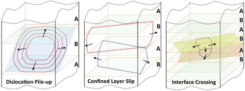
Layer thickness is a microstructural parameter in determining the mechanical properties of laminated composites because the predominant deformation mechanism in a laminate changes with decreasing thickness of the constituent layers [Citation3,Citation36]. Assuming that a certain interface acts as a barrier for the continuous motion of lattice dislocations, the development of plastic deformation requires high local stresses that act on the dislocation to overcome the barrier. Corresponding to this theoretical assumption, the dislocation pile-up-based Hall–Petch scaling law [Citation8,Citation37–43],h−1/2 (
is the flow strength and h is the layer thickness), is applicable at h greater than ∼100 nm, varying with the properties of constituent phases ((a)). For h in the range of approximately ∼10 to ∼100 nm, dislocation pile-up on the same plane is unlikely due to the strong repulsion among like-sign coplanar dislocations. The dominant deformation mechanism is confined layer slip (CLS) [Citation25,Citation44–49] that involves the propagation of single dislocation loops parallel to the interfaces within layers ((b)). At h less than approximately 10 nm, experimental data on a variety of metallic nanolaminates indicate that the hardness or strength of laminated materials [Citation3,Citation8,Citation36,Citation45] shows no significant increase in the flow strength with decreasing h. This behavior has been interpreted as a change in dominant deformation mechanism from CLS to interface crossing of single dislocations ((c)). The interface barrier strength to the transmission of a single glide dislocation, without the mechanical advantage of a dislocation pile-up, is largely dependent on interface structures and properties, while being independent of the layer thickness, but may drop when the layer thickness is on the order of dislocation core dimension [Citation27,Citation29,Citation50–58].
Figure 1. Predominant deformation mechanisms in laminated A/B composites: dislocation pile-up, confined layer slip, and interface crossing, with respect to layer thickness. Arrows indicate the motion direction of dislocations.
2.2. Crystallography of the layers
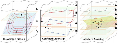
The crystallography of the layers defines the geometric relations of slip systems (slip planes and slip vectors) in the adjacent layers with respect to the interface plane. The transmissibility of slip across an interface is related to the degree of continuity of slip planes and slip vectors across the interface. It is widely accepted that the occurrence of slip transmission is geometrically favored when a slip system of a crystal on one side of the interface is well-aligned with a slip system of the adjacent crystal. Thus, a geometric factor can be introduced to describe the extent of the slip continuity. If we let κ be the minimum angle between their Burgers vector and θ the minimum angle between the traces that the slip plane makes with the interface ((a)), then an efficient transmission pathway would be defined as the value of
(1)
equal to or close to unity, where the angles θc and κc are the limiting angles for κ and θ, respectively[Citation59]. The angle θc is reasonably estimated to be ∼15 degrees corresponding to the bow-out of a 1∼2 nm long dislocation segment which is pinned by the neighboring glide planes. The angles κc may be larger, approximately 60 degrees. This leads to transferring most components of the Burgers vector of the incoming dislocation into the adjacent layer. According to Equation (1), when either κ or θ exceeds their corresponding thresholds, direct transmission is not possible unless the incoming dislocation line climbs in the interface to be parallel to the trace of the slip plane in the adjacent crystal. In addition, slip transmissibility is also dependent on stresses and energy barriers associated with the transmission of a dislocation across the interface. The Schmid factor of the outgoing slip system
that determines the glide direction leads to a modification of Equation (1) to
. The difference in slip vectors of the paired slip systems associated with the transmission would lead to transmission anisotropy between two layers because of the energy penalty associated with the residual dislocation at the interface after slip transmission.
Figure 2. The crystallography of slip across interface: (a) general case, (b) parallel slip systems case, and (c) twin-oriented case. The arrows indicate the glide direction of lattice dislocations under compression normal to the interface.
For laminates that share the same crystal structure and the same crystallographic orientation, the slip planes and slip vectors are nearly continuous across the interfaces ((b)), that is, κ = 0 and θ = 0. Thus χ = 1. For example of Cu/Ni and Cu/Ag systems that hold the cube-on-cube orientation relation [Citation17,Citation18,Citation30,Citation39,Citation51,Citation60–62], a small change in the magnitude of the slip vector at the interface poses a very minor resistance (or energy penalty) to slip, relative to the strength levels achievable in these materials. The strengthening effect in such kind of materials is thus ascribed to coherency stresses associated with the coherent interface as in Cu–Ni [Citation29,Citation50]. However, Cu–Ag does not have coherency stresses due to large lattice misfit and the slip transmission barrier is derived from the grid of misfit dislocations at the interface. When the two crystals hold the twin orientation relation, for example, eutectic Cu/Ag laminated composites with the twin orientation [Citation63–65] or nanotwinned metals[Citation66–72], the slip planes and slip vectors are of the mirror symmetry across the interface ((c)), that is, >
and θ = 0. Thus χ = 0. In addition, resolved shear stresses on both slip systems have mirror symmetry across the interface under a given applied stress; slip transmission is thus suppressed because of the negative
associated with the outgoing slip system. High strength in these materials is thus attributed to the discontinuity of the slip system.
For laminates that are composed of dissimilar crystal structures, the discontinuity of slip systems intrinsically exists in terms of slip planes and slip vectors. For example, in the Cu/Nb system, the large difference in the slip vectors (associated with a full dislocation in Nb and a partial dislocation in Cu) favors slip transmission from Nb to Cu, while opposing slip transmission from Cu to Nb [Citation27,Citation53]. Correspondingly, the flow strength is determined with respect to slip transmission from Cu to Nb. In addition, the crystallographic orientation influences the active slip systems within the individual nanolayers. For example, in bcc/hcp systems (Mg/Nb nanolaminates), the {0001}Mg||{110}Nb interface is thermodynamically favored [Citation73–75]. The primary slip system {0001}<1120> (referred to as basal slip) in a hexagonal close-packed (hcp) structure is suppressed because of the zero Schmid factor when the laminate is subjected to loading normal to the interface. Non-basal slip systems with higher critical resolved shear stresses (CRSSs) compared to basal slip thus accommodate plastic deformation in Mg nanolayers [Citation76–80]. Correspondingly, the Mg/Nb nanolaminates show unusually high flow strength, about five times higher than bulk Mg [Citation73].
2.3. Combination of constituent phases
An appropriate combination of constituent phases enables the optimization of strength and ductility of laminated materials. According to plastic deformation mechanisms of constituent phases, laminated materials can be categorized into three groups (). Both constituent phases in groups 1 and 2 are crystalline and plastically deform via nucleation and propagation of dislocations. For group 1, the CRSS for slip in both phases is similar (e.g. metal–metal nanolaminates). But for group 2, the CRSS in one constituent phase is much higher than that in the other, for example, metal-hard phase where ‘hard phase’ is crystalline ceramic or intermetallic. Unlike groups 1 and 2, group 3 is composed of one crystalline phase that plastically deforms via dislocations, and the other amorphous phase wherein STZs or shear bands accommodate plastic deformation.
Figure 3. Maximum strength of nanolaminated materials with respect to the combination of constituent phases: (a) metal–metal crystalline laminates (b) metal-crystalline hard phase laminates, and (c) metal-metallic glass laminates. Black squares indicate the strength of constituent 1 under the black line and red circles represent the strength of constituent 2 above the black line in the horizontal axis. Blue triangles represent the strength of nanolaminated composites.
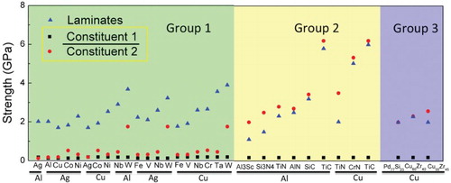
shows the maximum strengths of laminated composites with respect to the combination of constituent phases. For comparison, the maximum strength of each constituent phase refers to the strength of the bulk single crystal form. The strength of group 1 nanolaminates is higher than that of each constituent counterpart, (2) Group 2 nanolaminates have strengths in between the strengths of the two constituent counterparts, and (3) Group 3 nanolaminates can reach the yield strength of a single amorphous phase.
The unusually high strength achieved for group 1 nanolaminates can be accounted for based on three strengthening mechanisms with respect to three types of interfaces. Type 1 interface is fully coherent and generally occurs in very fine layers. Coherency stresses resulting from lattice mismatch must be overcome in order to achieve slip transmission [Citation29,Citation52,Citation81]. Type 2 interface is twin interface that causes crystallographic discontinuity of the slip system, for example, corresponding to the twin orientation strengthening mechanism [Citation63–72]. Type 3 interface is semi-coherent that has a low shear resistance in general, corresponding to weak shear interface strengthening mechanisms [Citation27,Citation28,Citation50,Citation53,Citation54,Citation57,Citation82]. It is worth pointing out that a general rule of mixtures in terms of materials strength breaks down in these nanolaminates.
In group 2 and 3 nanolaminated materials, the soft metal phases are strengthened, while the hard phases are softened. This can be accounted for by dislocation–interface interactions. In order to maintain the geometric compatibility of a laminated microstructure during straining, the elastic and plastic deformation in layers can be rationalized as follows. When a laminate is subjected to normal compression, plastic deformation first commences in softer layers and more plastic deformation develops in softer layers because of the lower yield strength and higher mobility of dislocations in the soft phase compared to the hard phase. Dislocations glide in the layers confined by the bounded interfaces, and deposit interface dislocations at the interfaces. The deposited dislocation arrays at interfaces produce residual stresses: tensile () in harder layers and compressive (
) in softer layers ((a)) [Citation83]. Both increase with the increase in the density (
) of the accumulated interface dislocations. The density
increases as the total deformation increases. Continuous deformation requires an increase in the applied loading in order to overcome the residual compressive stress in the softer layer, resulting in strain hardening of the softer phase. While the residual tensile stress in harder phases and the interaction force between these deposited dislocations at the adjacent interfaces produce a positive resolved shear stress ((b)), these reduce the required applied stress for activating dislocations in the harder layers. Due to plastic co-deformability, the group 2 nanolaminates exhibit high strength and plasticity.
Figure 4. Stress fields in 10 nm Al—5 nm TiN in association with the deposited interface dislocations with the average spacing of 10 nm, showing (a) the normal stress parallel to the interface and (b) the resolved shear stress with respect to a glide plane (denoted as dashed white lines) [Citation83].
![Figure 4. Stress fields in 10 nm Al—5 nm TiN in association with the deposited interface dislocations with the average spacing of 10 nm, showing (a) the normal stress parallel to the interface and (b) the resolved shear stress with respect to a glide plane (denoted as dashed white lines) [Citation83].](/cms/asset/9867a3c5-fd6e-4538-93c2-28c90913e2d5/tmrl_a_1225321_f0004_c.jpg)
For group 3 crystal-amorphous nanolaminated composites, plastic deformation in amorphous layers (specifically in metallic glasses) is mainly carried out by STZs at small strains and shear banding at large strains [Citation84–89]. The deposited dislocations activate STZs in amorphous layers, and further deformation increases the density of STZs, resulting in shear banding in amorphous layers. Since the metal–amorphous interfaces are less ordered, the incoming lattice dislocations are smeared along the interface, reducing the local strain/stress concentration [Citation82,Citation90–96]. The maximum strength that metal–amorphous nanolaminates can reach is mainly determined by the yield strength of the single amorphous phase [Citation97–100], although the nanolaminate composites exhibit plasticity.
2.4. Structures and properties of interfaces
Interfaces play triple roles in plastic deformation: sources for nucleating dislocations, barriers for impeding the motion of dislocations, and platforms for dislocation reactions. In group 1 laminated composites, interfaces play an obvious strengthening role: the strength of the composites is higher than that of each constituent phase. In group 2 and 3 laminated materials, the constraint from the layered geometry leads to induced plasticity in the hard phase facilitated by accumulated interface dislocations.
The difficulty of dislocation transmission through an interface is ascribed to different mechanisms with respect to interface types. For coherent interface, coherency stresses play a crucial role in defining the maximum strength that can be achieved ((a)). The strength model suggested by Hoagland et al. [Citation29] is based on the idea that a dislocation cannot traverse the composite unless the net forces on the dislocation in all layers are the same sign. Thus, a stress must be applied that at least cancels the coherency stress in one of the two constituents. In systems such as Cu–Ni with equal layer thickness, the calculated coherency stresses are on the order of 2 GPa, comparable to the experimentally measured strengths [Citation8,Citation28,Citation60]. For twin boundary in single-phase or bi-phase metals [Citation63–72], the change in crystal orientations between matrix and twinned crystals [Citation101] results in the discontinuity of slip systems across twin boundaries ((b)) [Citation102,Citation103]. Consequently, a high resolved shear stress is required to transmit a single dislocation across twin interfaces, thereby increasing the strength [Citation67,Citation68,Citation104–110].
Figure 5. Schematic of key strengthening mechanisms in nanolaminates: (a) coherency stresses associated with lattice-matched nanolayers, (b) discontinuity of slip across twin interface, (c) glide dislocations pinned by grid of misfit dislocations at a semi-coherent interface, and (d) cross-slip of lattice dislocation in the weak shear interface.
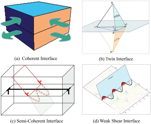
A semi-coherent interface is composed of patches of atomic coordination separated by misfit dislocations that relax the long-range coherency stresses. The arrays of misfit dislocations at interfaces must be cut (c) for a single dislocation transmission across the interface [Citation30,Citation55]. Because of the intrinsic discontinuity of slip across a semi-coherent interface, slip transmission naturally involves a re-nucleation process, as demonstrated in Cu–Nb multilayers using atomistic simulations [Citation27,Citation28,Citation111]. More importantly for a semi-coherent interface, interfaces show lower shear resistance than the theoretical estimates of shear strengths on glide planes in perfect crystals, because intersections of misfit dislocations act as preferred sites for nucleating an interface dislocation loop [Citation27,Citation28,Citation53,Citation54,Citation57]. As a consequence, the interface will shear in response to the stress fields of a nearby lattice dislocation and attract the dislocation into the interface [Citation27,Citation28,Citation112]. After the incoming dislocation becomes absorbed and extends its core within the interface plane, in order for it to transmit into the other crystal, it must then ‘re-nucleate’ and bow-out onto the outgoing slip system, an event that is aided by thermal activation [Citation28,Citation111]. Using atomistic simulations, it has been demonstrated that a dislocation, no matter what type or sign, spontaneously enters the interface, due to the shear of the interface. The core of the lattice glide dislocation readily spreads within the interface, resulting in a nonplanar core structure. The width of core spreading increases with decreasing interface shear strength [Citation27]. Thus, core spreading effectively pins a glide dislocation in the interface plane and so ‘weak shear’ interface can be a very strong barrier to slip transmission across interfaces ((d)). Atomistic simulations [Citation111] demonstrated that the weaker the interface, the larger the magnitude of core spreading, and hence stronger resistance to slip transmission, as shown in .
Figure 6. The maximum resolved shear stress required to accomplish the slip transmission as a function of interface shear strength [Citation111].
![Figure 6. The maximum resolved shear stress required to accomplish the slip transmission as a function of interface shear strength [Citation111].](/cms/asset/5fcbe5e2-7dec-45a4-98c0-4a4dd7b552c4/tmrl_a_1225321_f0006_c.jpg)
The ability of an interface to transmit dislocations may change with strain. Over the duration of plastic deformation, the interface must interact with a high flux of dislocations. These dislocations either become stored in the interface or transmit across it. Even if they were to transmit, residual dislocations are deposited in the interface since the Burgers vectors of the incoming and outgoing dislocations are unequal. Thus either way, dislocation–interface interactions can increase the extrinsic dislocation density stored in the interface with applied strain. In the event that this extrinsic density is not recovered, it can affect the ability of the interface to transmit subsequent dislocations. It can be envisioned that this density could, on the one hand, repel subsequent dislocations, thereby hindering transmission, or, on the other hand, it can increase the interfacial shear strength, thereby promoting transmission with strain [Citation27,Citation59,Citation111,Citation112].
3. Plasticity in interfaces
Plastic deformation in nanolaminated materials involves plasticity in the interface as well as the constituent layers. Interface plasticity is accomplished through nucleation, glide, and climb of dislocations that lie in the interface plane. Thus, it is controlled by the interface structures and properties.
3.1. Glide of interface dislocations
Interface shear occurs via nucleation and glide of interface dislocations under effective shear stresses parallel to the interface plane [Citation54]. In addition to interface sliding under applied shear stress, interface shear can be triggered by the creation of interface dislocations under the stress field associated with lattice glide dislocations impinging on the interface [Citation27,Citation56,Citation82,Citation113,Citation114]. The created interface dislocations further attract lattice dislocation into the interface. The in-plane component of Burgers vector of the lattice dislocation then spreads along the interface (corresponding to the core spreading), causing interface shear. A glide dislocation blocked by the interface can also cross-slip into the interface plane without core spreading, especially if the interface plane is also a glide plane, resulting in interface sliding [Citation27,Citation82,Citation112].
3.2. Climb of interface dislocations
Interface dislocations can climb along the interface plane because of the low formation energy and low migration energy of point defects in interface [Citation53,Citation59,Citation69,Citation115–127], as demonstrated by molecular dynamics (MD) simulations [Citation116–127]. In particular for a semi-coherent interface, point defects have lower formation energy and lower migration energy along misfit dislocation lines and at intersections of misfit dislocations [Citation59,Citation124–127]. Thus, an interface has higher equilibrium concentration for point defects. Dislocation climb at the Cu–Nb interface has been inferred from atomistic simulations ((a)) [Citation123] and experimentally observed in Al–Nb interfaces ((b1–b3)) [Citation115]. This is consistent with a high vacancy concentration and a high diffusivity of vacancies in these interfaces. Atomistic Monte Carlo simulations indicate that the Cu–Nb interface can have a high vacancy concentration of 0.05 (c), about 14 orders of magnitude higher than the vacancy concentration in the bulk Cu crystal [Citation58]. The mean extended vacancy formation Ef with respect to the removal of atoms in the interfacial Cu layer is computed to be 0.12 eV/atom. This formation energy is one order of magnitude smaller than the formation energies of vacancies (1.26 eV) or interstitials (3.24 eV) in bulk Cu. In addition, the migration of a point defect in the interfacial plane involves the rearrangement of a group of atoms with an associated delocalized displacement field within the interface, unlike single-atom jumps for a vacancy in a bulk crystal. Using the Nudged Elastic Band method, the kinetic barriers associated with the migration from one delocalized displacement field to the other were computed in the range of 0.03–0.10 eV by molecular statics simulations. This small kinetic barrier is comparable with a Cu adatom diffusing on a flat Cu (111) surface [Citation128–131], and results in the high diffusivity of vacancies within interfaces. Similar results have been observed in Cu–Ni and Cu–Ag interfaces [Citation59].
Figure 7. (a) Molecular dynamics simulations demonstrated dislocation climb along the Cu–Nb interface [Citation123], and (b1–b3) in situ TEM observations of dislocation climb along the Al–Nb interface [Citation115]. Climb of the out-of-plane component of interfacial dislocations is ascribed to (c) a high equilibrium vacancy concentration of 5.8% at 300 K and a low kinetic barrier of 0.03–0.10 eV for vacancy migration in the interface [Citation55,Citation128].
![Figure 7. (a) Molecular dynamics simulations demonstrated dislocation climb along the Cu–Nb interface [Citation123], and (b1–b3) in situ TEM observations of dislocation climb along the Al–Nb interface [Citation115]. Climb of the out-of-plane component of interfacial dislocations is ascribed to (c) a high equilibrium vacancy concentration of 5.8% at 300 K and a low kinetic barrier of 0.03–0.10 eV for vacancy migration in the interface [Citation55,Citation128].](/cms/asset/25a2f17a-417a-4363-b4ef-fe69d5b52d9a/tmrl_a_1225321_f0007_c.jpg)
Because of the easy glide and efficient climb, interfacial dislocations can move within the interface, react with other interfacial dislocations, and interact with point defects in the interface. First, the easy glide and efficient climb enable slip transmission: glide dislocations can reassemble the spread cores in the interface plane via climb, and dislocation debris scattered in interfaces can reassemble into lattice glide dislocations, facilitating slip transmission. Second, reactions between interfacial dislocations assisted by glide and climb could lead to the annihilation of dislocation content (recovery) ((b)). Third, discrete pile-ups can be absorbed in the interface plane, assisted by glide and climb in the interface, thereby blunting the stress concentration of the pile-up [Citation28,Citation122]. Finally, dislocation climb enables the interfacial plane to be in an equilibrium state with respect to concentrations of point defects because of absorption and/or emission of vacancies at dislocation cores. Thus, semi-coherent interfaces offer an ideal platform for the dynamic recovery and reassembly of interface defects. Nanolaminated materials could persist in a damage-free steady state even when driven far from equilibrium by intense particle radiation [Citation5,Citation26,Citation28,Citation55,Citation122].
3.3. Effect of interface dislocations on strain hardening in metallic nanolaminates
When the incompatibility of plastic deformation in the adjacent layers is small, strain hardening is mainly ascribed to the character of accumulated interface dislocations and interface mechanical properties. For example, nanotwinned face centered cubic (fcc) metals show a high strain hardening rate than Cu–Nb multilayers ((a)). This is ascribed to the high density of accumulated interface dislocations in twin boundaries that originate from the crystallography of slip in the layered microstructure ((b)), but the less accumulated dislocations in the Cu–Nb interface because of the dynamic recovery of dislocations assisted by the efficient climb and glide in the Cu–Nb interface [Citation58,Citation115,Citation123,Citation132]. By fitting experimentally measured stress–strain curves in the function form of = K1 + K2
, the coefficient K2 represents the increment in flow strength due to unit increase in strain. For nt Cu, K1 = 760 MPa, K2 = 580 MPa, and n = 0.12 [Citation103]. For comparison, the values of fitting constants to work hardening results in rolled bulk Cu and 2.5 nm Cuss/2.5 nm Nb multilayers [Citation133] are K1 = ∼0 MPa, K2 = 350 MPa and n = 0.35 and K1 = 2250 MPa, K2 = 100 MPa, and n = 0.05, respectively. The value of K1 is significantly higher in nanotwinned Cu than that of bulk Cu as a result of higher flow strength of the nt Cu, and is lower than that of the 2.5 nm Cu/2.5 nm Nb multilayer. The strain hardening rates are calculated to be 10 GPa for bulk Cu, 0.9 GPa for nt Cu, and 0.09 GPa for 2.5 nm CuNb multilayers at the strain level of ∼5%. It is also noticed that a higher strain hardening rate was measured experimentally, 7 GPa in 30 nm Cu/30 nm Nb multilayers at the strain of ∼5%, but the flow strength is lower than the 2.5 nm Cu/Nb multilayers [Citation103].
Figure 8. (a) Measured true stress—strain curve of nanotwinned Cu foils. (b) Cross-sectional TEM micrographs of nanotwinned Cu films after 50% thickness reduction, showing a high density of dislocations along twin boundaries without dislocation cell walls in layers [Citation103]. (c) The crystallography of slips in nanotwinned multilayers shows three paired {111} slip systems across the twin interface. (d) Lomer dislocations at the twin interface as a reaction result of the deposited interface dislocations. (e) The crystallography of slips in the KS fcc–bcc system shows three paired {111} slip systems across the interface. (f) A small residual dislocation results from the reaction of the deposited interface dislocations.
![Figure 8. (a) Measured true stress—strain curve of nanotwinned Cu foils. (b) Cross-sectional TEM micrographs of nanotwinned Cu films after 50% thickness reduction, showing a high density of dislocations along twin boundaries without dislocation cell walls in layers [Citation103]. (c) The crystallography of slips in nanotwinned multilayers shows three paired {111} slip systems across the twin interface. (d) Lomer dislocations at the twin interface as a reaction result of the deposited interface dislocations. (e) The crystallography of slips in the KS fcc–bcc system shows three paired {111} slip systems across the interface. (f) A small residual dislocation results from the reaction of the deposited interface dislocations.](/cms/asset/7c7a6f7c-c892-4023-aa5a-87ad5ead3180/tmrl_a_1225321_f0008_c.jpg)
The difference in strain hardening rate between nanotwinned Cu and CuNb multilayers is ascribed to the character of accumulated interface dislocations. The presence of twin interfaces causes the change in crystal orientations between matrix and twinned crystals, resulting in the discontinuity of slip systems across twin interfaces ((c)). When nanotwinned Cu is subjected to normal loading (perpendicular to the twin interface plane), lattice dislocations meet at the interface and react to form Lomer dislocations that cannot glide along the interface ((d)). In addition, shear stresses parallel to twin interfaces are minimal, or locally exist in some regions of twin interfaces due to the residual dislocations at twin interfaces. Therefore, these interface dislocations are likely to be sessile at twin interfaces, acting as stored dislocations which cause strain hardening. Unlike the twin interface, slip systems in CuNb multilayers can be paired to reduce the content of interface dislocations, as shown in (e) and (f). In particular, the low formation energy of point defects in the CuNb interface enables the dislocation climb along the interface [Citation58] and the low interface shear [Citation27,Citation82] facilitates glide of interface dislocations that facilitates the recovery of stored dislocation content. Using Synchrotron X-ray micro-diffraction, it was demonstrated that the content of interface dislocations does not increase significantly in CuNb nanolayers during straining up to a final cumulative strain of 35% [Citation132]. Thus, a relatively lower strain hardening rate was observed in CuNb multilayers.
3.4. Twin, slip, and shear banding in crystalline laminates
To demonstrate the correlation of the occurrence of plastic flow instability with the crystallography of slip systems and interface properties, two material systems Cu–Ag and Cu–Nb are compared.
Lamellar eutectic Cu–Ag, fabricated via a flux-melting technique, [Citation18, Citation65, Citation134, Citation135] exhibits two kinds of crystallographic relations, cube-on-cube and hetero-twin. Both share a semi-coherent {111}Cu||{111}Ag interface. An analysis of the crystallography of slip systems indicates three pairs of slip systems that share the same slip trace on the interface ((a) and (b)). The cube-on-cube orientation relationship retains the continuity of slip across the interface, while the hetero-twin orientation relationship results in the discontinuity of slip across the twin interface ((b), also see (d)). As a consequence, the paired slip systems across the interface will annihilate the common Burgers vectors in the cube-on-cube Cu–Ag interface. A very small residual Burgers vector (0.034 nm, approximately 1/10th of the full Burgers vector) is left on the interface. However, the paired slip systems in the hetero-twin Cu–Ag only annihilate the in-plane components, and a large residual Burgers vector (0.221 nm, 86% of full Burgers vector) is left on the interface as a Lomer sessile dislocation ((d)).
Figure 9. (a) High-resolution transmission electron microscope (HRTEM) image of a typical cube-on-cube Cu–Ag interface and (b) fine twin bands in the cube-on-cube Cu–Ag composite. (c) HRTEM image of a typical hetero-twin Cu–Ag interface and (d) a shear band in the hetero-twin Cu–Ag composite. Three paired slip systems form the threefold crystallographic symmetry of slip systems about the normal of the interface [Citation65].
![Figure 9. (a) High-resolution transmission electron microscope (HRTEM) image of a typical cube-on-cube Cu–Ag interface and (b) fine twin bands in the cube-on-cube Cu–Ag composite. (c) HRTEM image of a typical hetero-twin Cu–Ag interface and (d) a shear band in the hetero-twin Cu–Ag composite. Three paired slip systems form the threefold crystallographic symmetry of slip systems about the normal of the interface [Citation65].](/cms/asset/fe20936b-be46-4ef3-a6e0-c7cc80a96970/tmrl_a_1225321_f0009_c.jpg)
It is noticed that three paired {111} slip systems hold a threefold symmetry around the normal of the interface in both cube-on-cube and hetero-twin orientation relationships ((a) and (c)). When the materials are subjected to the loading (perpendicular to the interface plane), the Schmid factor is 0.32 for all glide dislocations on {111}-type glide planes [Citation65]. Therefore, the activity of dislocations is assumed to be the same on all {111}-type planes. If the same number of slip systems and the same slip activity on all glide planes are activated in both Cu and Ag, plastic deformation can take place in a symmetrical mode in both crystals across the interface. As a result, there is no net rotation of the (111) interface, although the residual dislocations are accumulated on the interface. However, the activation of dislocations in Ag is easier than Cu and twinning commonly occurs in Ag. This causes the development of stress concentrators along the interface. With continuous straining, twins in Ag layers transmit into Cu layers in the cube-on-cube Cu–Ag laminates. Once one twinning system is predominated, the other two twinning systems will be either completely suppressed or have lower activity, and plastic flow instability occurs accompanied by the propagation of twin bands across multiple layers. Within this cross-interface twin band, the pair of twinning systems on either side of the interfaces is well-aligned and the cube-on-cube orientation relation is maintained within the band[Citation65]. This localized twin band may be classified as crystallographic ((b)).
Differing from the cube-on-cube Cu–Ag laminates, the residual dislocations resulting from paired {111} slip systems across the twin boundary are Lomer dislocations that have Burgers vector perpendicular to the twin interface in the hetero-twin Cu–Ag laminates (also see (d)). In the absence of a symmetrical activation of three sets of paired slip systems, the accumulation of Lomer dislocations causes interface tilting, facilitating cross-slip of dislocations on the twin interface. This local change in slip activity could favor large crystallographic rotations and lead to shear banding ((d)) in the hetero-twin Cu–Ag system [Citation65]. In the central core zone of the shear band, the layered morphology is preserved, the layer thickness has become finer, and the layers have rotated relative to those in the matrix. The shear band structure is not aligned with any crystallographic plane, indicating non-crystallographic banding [Citation65,Citation134].
Similar phenomena have also been observed in Cu–Nb laminates. Cu–Nb thin films produced by PVD [Citation20,Citation65,Citation136] possess planar Cu–Nb interfaces with a KS orientation relationship ((a)). Using micropillar compression, non-crystallographic shear banding occurs and runs across the pillar wherein the layers had rotated to an orientation favorable for interfacial sliding ((b)) [Citation20,Citation65,Citation136]. The KS orientation relationship is preserved, but altogether the Cu and Nb crystallographic orientations have reoriented by 28.5°, while the morphology of the Cu–Nb interface has only rotated 17.5°. The difference signifies that the crystallographic interface planes have tilted 11° and no longer correspond to the {111}Cu||{110}Nb planes [Citation65,Citation136]. Thus, like the hetero-twin Cu–Ag interface, a shear band is associated with an interface that is resistant to dislocation transmission. It is noticed that an approximate threefold symmetry of paired slip systems is preserved in the KS orientation relationship (also see (e)). The instability of plastic flow is ascribed to the easy shear interface [Citation27,Citation28,Citation50,Citation54,Citation57,Citation82,Citation111] and the interface tilting which is triggered by the accumulated residual defects associated with the difference in slip vectors [Citation65]. It is worth pointing out that the local stress state may change the deformation mode, although the approximate threefold symmetry of paired slip systems is preserved. Using the nanoindentation technique, the local shear stress favors one paired slip system than other two pairs; as a consequence, twinning is activated in the Cu layer by slip transmission from the Nb layer [Citation136]. Under shock loading, Han et al. observed many twins in Cu layers due to the heterogeneous stresses [Citation137].
Figure 10. (a) HRTEM image of a typical KS Cu{111}–Nb{110} interface and (b) a shear band in the composite [Citation65]. (c) HRTEM image of a typical KS Cu{112}–Nb{112} interface and (d) a shear band in the composite. The white lines in (a) and green lines in (c) indicate the favorably paired slip systems. (e) and (f) TEM images of (d), showing fine twins and stacking faults in the Cu layer that are parallel to the favorably paired slip plane.
![Figure 10. (a) HRTEM image of a typical KS Cu{111}–Nb{110} interface and (b) a shear band in the composite [Citation65]. (c) HRTEM image of a typical KS Cu{112}–Nb{112} interface and (d) a shear band in the composite. The white lines in (a) and green lines in (c) indicate the favorably paired slip systems. (e) and (f) TEM images of (d), showing fine twins and stacking faults in the Cu layer that are parallel to the favorably paired slip plane.](/cms/asset/46e60377-4f35-417f-aa9b-f197f8119fd4/tmrl_a_1225321_f0010_c.jpg)
Cu–Nb nanolaminates fabricated by ARB [Citation15,Citation21,Citation23,Citation25], however, contain crystallographically different interfaces that are more resistant to interface sliding [Citation138,Citation139] and preserve favorable paired slip systems (c). Interestingly comparing the electron diffraction patterns within the as-prepared material and the band in the deformed material, it is found that the crystals have not rotated with the band [Citation65]. Within the band, the orientations of the (111)Cu and (10)Nb planes θcu and θNb with respect to the fixed x-axis are distributed within (18–27°) and (23–38°), respectively ((d)). These ranges are very similar to those found in the as-prepared material, that is, (16–24°) and (24–35°). The misorientation across the interface is also preserved. Further, the band angle β of ∼25° lies within the ranges of θCu and θNb for the pair of (111)Cu-(10
)Nb slip planes, the most well-aligned for slip transmission across the interface ((c) and (f)). In particular, fine twin bands and high density of stacking faults were observed in the Cu layers ((e)). Taken together, the above findings suggest that this plastic instability occurred via successive dislocation transmission across the interfaces on the well-aligned (111)Cu-(10
)Nb slip planes, leading to the formation of a slip band.
In summary, the transmissibility of the interface and interface shear resistance profoundly change the mode of strain localization. When the interface permits the transmission of slip or twin, crystallographic slip or twin bands occur. However, if the interface blocks impinging dislocations from transmitting, the accumulation of extrinsic interface dislocations causes interface plane rotation. The tilt can promote dislocation cross-slip on the interface and interface sliding, which are believed to lead to non-crystallographic shear banding.
3.5. Shear banding in crystal-amorphous laminates
Metal/amorphous laminated composites have been fabricated in pursuit of enhanced mechanical and functional properties of amorphous layers in the recent years [Citation84–90,Citation97–100,Citation140–153]. The amorphous layer involves metallic glasses [Citation84–90,Citation97–100,Citation140–145], amorphous ceramics [Citation146–151], and carbon or silicon family elemental glasses [Citation152–157]. To conquer mechanical instabilities of amorphous materials, the laminated microstructure constrains the formation and propagation of damage (cracks and shear bands) in amorphous layers and possibly enables the plastic co-deformation between amorphous and metallic layers. The study of mechanical deformation of metal/amorphous laminated composites has been largely focused on the metal-metallic glass and metal–amorphous ceramic laminates [Citation84–90,Citation97–100, Citation140–155]. Plastic deformation in metal–amorphous laminates, unlike crystalline laminates, is mainly accommodated by plastic deformation in metallic layers. The mechanical behavior of amorphous materials is dependent on their category. Amorphous metals (or metallic glasses) lack strain hardening ability, resulting in limited elongation after the elastic–strain region [Citation85–90,Citation140–145]. Beyond the elastic limit, metallic glasses deform via STZs and fail by localized shear bands [Citation140–145].
Amorphous ceramics behave very similarly to crystalline ceramics at room temperature which fails by brittle fracture [Citation150,Citation151]. An experimental study of an Al-amorphous SiC system [Citation150] revealed the mechanical instability associated with the fracturing of the SiC layers in the nanolaminate at large deformations [Citation151], although nanoscale amorphous SiC layers demonstrated remarkable elastic bending flexibility. The interface bonding strength of the Al-amorphous SiC was found to be higher than the rupture strength of pure Al. This is evident as cracks initiate inside Al layers instead at the interface [Citation151]. Plastic co-deformation between the Al and amorphous SiC layers could not be achieved [Citation150, Citation151].
Unlike metal–amorphous ceramics laminates, plastic co-deformation has been observed in metal-metallic glass when the thickness of the layers is carefully tuned [Citation84–90,Citation97–100,Citation141–145]. Taking Cu/CuZr glasses as a prototype material, their laminated films were deposited with alternating layers of amorphous CuZr and crystalline Cu layers [Citation141–145]. Cui et al. performed a series of experimental study [Citation141] in which Cu layers had a thickness of 18 nm in all multilayers, and CuZr layers had different thicknesses of 4, 10, 20, 40, 75, and 100 nm, respectively. Scanning electron microscope images of the laminates after the indentation testing revealed the formation of shear bands as the CuZr layer thickness exceeds 20 nm, while a homogenous plastic deformation in the 4 nm CuZr—18 nm Cu and the 10 nm CuZr—18 nm Cu multilayers [Citation141]. shows the cross-sectional transmission electron microscope images of the 40 nm CuZr—18 nm Cu multilayer. In (a), we marked six shear bands in the rectangles, SB1 to SB6. Four intriguing features are characterized. (1) Shear bands did not nucleate from surfaces of the samples; (2) shear bands cut through several crystalline and amorphous layers; (3) localized shear in the Cu layers is accomplished via slip on {111} planes; and (4) shear bands are approximately parallel to the {111} plane in the Cu layers (nonparallel to interface plane). In this scenario, slip bands are triggered in the Cu layers to accommodate the localized shear deformation associated with the extension of shear bands in the CuZr layers, as observed in (c) and (d), and schematically illustrated in .
Figure 11. TEM images of the 40 nm CuZr/Cu multilayer after indentation testing. (a) Six shear bands outlined in the yellow rectangles and (b) the shear bands SB1 and SB2 end at the CuZr–Cu interfaces. (c) and (d) slip bands in the Cu layers that formed associated with shear on {111} planes nonparallel to the layers. The thin red line in (c) and (d) represents {111} planes in the Cu. Two tilt grain boundaries, GB1 and GB2, are marked in (c), indicating that shear also occurs on the {111} plane parallel to the layers. The regions outlined by the yellow circles show a crystalline structure in the CuZr.
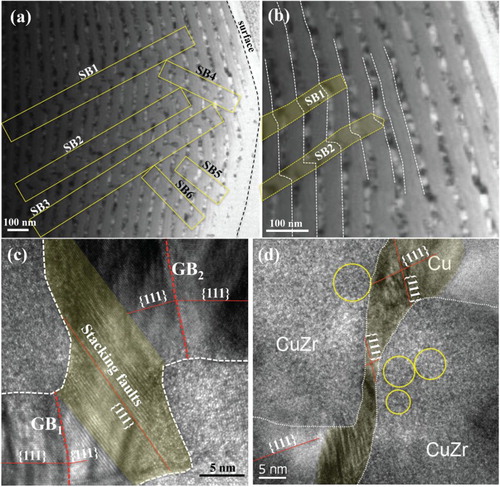
Figure 12. Schematics of plastic deformation modes with respect to the CuZr layer thickness. (a) Plastic co-deformation in the thin CuZr layers, showing plastic deformation in the Cu layers via slip on {111} planes and the formation and reaction of STZs in the CuZr layers. The red ellipses represent STZs. (b) The formation and propagation of shear bands in the thick CuZr layers, showing propagation of shear bands into the Cu layers, are accomplished via the formation of slip bands on {111} planes. The dashed lines represent {111} planes nonparallel to the layers.
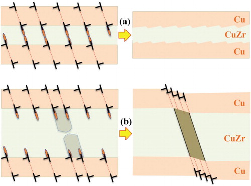
The lack of shear banding in the 4 nm and 10 nm CuZr/Cu multilayers could be understood according to plastic co-deformation mechanisms. Noted that there exists a critical length scale of 10–20 nm for amorphous CuZr alloys, below which amorphous CuZr layers can plastically deform via the so-called STZs [Citation84–90,Citation97–100,Citation141–145]. The deposited dislocations at interfaces act as stress concentrators, facilitating the formation of STZs at interfaces in CuZr layers and achieving plastic deformation transmission from the Cu layer to the CuZr layer, as illustrated in (a) and demonstrated by MD simulations [Citation90,Citation141].
With the increase in the CuZr layer thickness, the tensile stress in the CuZr layers and the interaction force between the deposited dislocations at the adjacent interfaces decrease. Even though STZs are formed at interfaces, the propagation of the STZs across the entire CuZr layer is slowed down due to the reduced shear stress on the plane nonparallel to the CuZr layers. When increasing the applied compressive stress, the resultant shear stress on the plane nonparallel to the CuZrlayers eventually triggers the formation of shear bands by gathering STZs in the CuZr layers. The formed shear bands then propagate toward the adjacent interfaces, and consequently trigger plastic deformation in the Cu layers. Corresponding to the crystallography of the Cu layer, slip on {111} planes via either Shockley partial dislocations or full dislocations accommodate the localized shear deformation in the adjacent CuZr layers. As a consequence, slip bands are formed in the Cu layers parallel to the {111} planes, constraining shear bands in the CuZr layers that are parallel to the {111} plane in the Cu layers. Accompanying the propagation of such shear bands, the shear stress in the front of the shear bands decreases, associated with the development of a zone of plastic deformation, and the shear bands are more likely to eventually stop propagation at the CuZr–Cu interfaces.
4. Summary
Due to a high density of interfaces, geometrical constraints from layered geometry, controllable layer thickness, designed interfaces (orientation relationship, atomic structure, and interface shear strength), and nanolaminated composites achieve a unique combination of mechanical properties—high flow strength, good ductility, thermal stability, and plastic flow stability at large strains. In particular, the mechanical behavior of nanolaminates is dominated by interfaces that act as sources, barriers, and preferred sites for storage and dynamic recovery of glide dislocations.
Theory and modeling at different length scales including atomistic [Citation27–29,Citation56,Citation72–74,Citation90,Citation91,Citation158], discrete dislocation dynamics [Citation159–168], and crystal plasticity [Citation169,Citation170], integrated with experimental observations, provide insights into understanding the interface- dominated behavior of nanolaminates. However, incorporating all of the relevant interface physics into the multiscale models to develop predictive capability is still a challenge [Citation53,Citation114].
Acknowledgements
JW and AM acknowledge research sponsorship by DOE, Office of Basic Energy sciences. SS acknowledges the start-up grant provided by the Louisiana State University. The authors acknowledge collaborations with J.P. Hirth, R.G. Hoagland, N.A. Mara, I.J. Beyerlein, N. Li at Los Alamos National Laboratory, H.J. Chu at Shanghai University, K. Kang at Yonsei University, S.J. Zheng at Shenyang National Laboratory for Materials, R.F. Zhang at Beihang University, and C.Z. Zhu at Missouri University of Science and Technology.
Disclosure statement
No potential conflict of interest was reported by the authors.
ORCiD
Jian Wang http://orcid.org/0000-0001-5130-300X
References
- Gleiter H. Nanostructured materials: basic concepts and microstructure. Acta Mater. 2000;48:1–29. doi: 10.1016/S1359-6454(99)00285-2
- Meyers MA, Mishra A, Benson DJ. Mechanical properties of nanocrystalline materials. Prog Mater Sci. 2006;51:427–556. doi: 10.1016/j.pmatsci.2005.08.003
- Misra A, Hirth JP, Hoagland RG. Length-scale-dependent deformation mechanisms in incoherent metallic multilayered composites. Acta Mater. 2005;53:4817–4824. doi: 10.1016/j.actamat.2005.06.025
- Launey ME, Munch E, Alsem DH, et al. A novel biomimetic approach to the design of high-performance ceramic–metal composites. J Roy Soc Int. 2010;7:741–753. doi: 10.1098/rsif.2009.0331
- Misra A, Demkowicz MJ, Zhang X, et al. The radiation damage tolerance of ultra-high strength nanolayered composites. JOM. 2007;59(9):62–65. doi: 10.1007/s11837-007-0120-6
- Nieh TG, Wadsworth J. High strength freestanding metal-amorphous multilayers. Scripta Mater. 2001;44:1825–1830. doi: 10.1016/S1359-6462(01)00801-6
- Liu BX, Lai WS, Zhang ZJ. Solid-state crystal-to-amorphous transition in metal/metal multilayers and its thermodynamic and atomistic modelling. Adv Phys. 2001;50:367–429. doi: 10.1080/00018730110096112
- Misra A, Verdier M, Lu YC, et al. Structure and mechanical properties of Cu-X (X = Nb,Cr,Ni) nanolayered composites. Scripta Mater. 1998;39:555–560. doi: 10.1016/S1359-6462(98)00196-1
- Johnson MT, Bloemen PJH, den Broeder FJA, et al. Magnetic anisotropy in metallic multilayers. Rep Prog Phys. 1996;59:1409–1458. doi: 10.1088/0034-4885/59/11/002
- Mahan JE. Physical vapor deposition of thin films. 1st ed. New York: Wiley; 2012.
- Was GS, Foecke T. Deformation and fracture in microlaminates. Thin Solid Films.1996;286:1–31. doi: 10.1016/S0040-6090(96)08905-5
- Ross CA. Electrodeposited multilayer thin films. Annu Rev Mater Sci. 1994;24:159–188. doi: 10.1146/annurev.ms.24.080194.001111
- Callister Jr WD. Materials science and engineering: an introduction. New York: Wiley; 1997. Chapter 9, Phase diagrams; p. 236–288.
- Lütjering G, Williams JC. Titanium. New York: Springer; 2007. Chapter 2, Fundamental aspects; p. 15–52.
- Carpenter JS, Vogel SC, Ledonne JE, et al. Bulk texture evolution of Cu–Nbnanolamellar composites during accumulative roll bonding. Acta Mater. 2012;60:1576–1586. doi: 10.1016/j.actamat.2011.11.045
- Tsuji N, Saito Y, Lee SH, et al. ARB (accumulative roll-bonding) and other new techniques to produce bulk ultrafine grained materials. Adv Eng Mater. 2003;5:338–344. doi: 10.1002/adem.200310077
- Shen TD, Schwarz RB, Zhang X. Bulk nanostructured alloys prepared by flux melting and melt solidification. Appl Phys Lett. 2005;87: article no. 141906. doi: 10.1063/1.2056610
- Wang J, Beyerlein IJ, Mara NA, et al. Interface-facilitated deformation twinning in copper within submicron Ag–Cu multilayered composites. Scripta Mater. 2011;64:1083–1086. doi: 10.1016/j.scriptamat.2011.02.025
- Li N, Wang J, Misra A, et al. Direct observations of confined layer slip in Cu/Nb multilayers. Microsc Microan. 2012;18:1155–1162. doi: 10.1017/S143192761200133X
- Mara NA, Bhattacharyya D, Dickerson P, et al. Deformability of ultrahigh strength 5 nm Cu/Nb nanolayered composites. Appl Phys Lett. 2008;92: article no. 231901. doi: 10.1063/1.2938921
- Lee SB, Ledonne JE, Lim SCV, et al. The heterophase interface character distribution of physical vapor-deposited and accumulative roll-bonded Cu–Nb multilayer composites. Acta Mater. 2012;60:1747–1761. doi: 10.1016/j.actamat.2011.12.007
- Zheng SJ, Beyerlein IJ, Carpenter JS, et al. High-strength and thermally stable bulk nanolayered composites due to twin-induced interfaces. Nat Commun. 2013;4: article no. 1696. doi: 10.1038/ncomms2651
- Carpenter JS, Zheng SJ, Zhang RF, et al. Thermal stability of Cu–Nbnanolamellar composites fabricated via accumulative roll bonding. Philos Mag. 2013;93:718–735. doi: 10.1080/14786435.2012.731527
- Misra A, Hoagland RG, Kung K. Thermal stability of self-supported nanolayered Cu/Nb films. Philos Mag. 2004;84:1021–1028. doi: 10.1080/14786430310001659480
- Anderson PM, Bingert JF, Misra A, et al. Rolling textures in nanoscale Cu/Nb multilayers. Acta Mater. 2003;51:6059–6075. doi: 10.1016/S1359-6454(03)00428-2
- Demkowicz MJ, Hoagland RG, Hirth JP. Interface structure and radiation damage resistance in Cu-Nb multilayer nanocomposites. Phys Rev Lett. 2008;100: article no. 136102. doi: 10.1103/PhysRevLett.100.136102
- Wang J, Hoagland RG, Hirth JP, et al. Atomistic modeling of the interaction of glide dislocations with ‘weak’ interfaces. Acta Mater. 2008;56:5685–5693. doi: 10.1016/j.actamat.2008.07.041
- Wang J, Misra A. An overview of interface-dominated deformation mechanisms in metallic multilayers. Curr Opin Solid State Mater Sci. 2011;15:20–28. doi: 10.1016/j.cossms.2010.09.002
- Hoagland RG, Mitchell TE, Hirth JP, et al. On the strengthening effects of interfaces in multilayer fcc–metallic composites. Philos Mag. 2002;82: 643–664.
- Mckeown J, Misra A, Kung H, et al. Microstructures and strength of nanoscale Cu–Ag multilayers. Scripta Mater. 2002;46:593–598. doi: 10.1016/S1359-6462(02)00036-2
- Han WZ, Cerreta EK, Mara NA, et al. Deformation and failure of shocked bulk Cu–Nb nanolaminates. Acta Mater. 2014;63:150–161. doi: 10.1016/j.actamat.2013.10.019
- Mara NA, Bhattacharyya D, Hoagland RG. Tensile behavior of 40 nm Cu/Nb nanoscale multilayers. Scripta Mater. 2008;58:874–877. doi: 10.1016/j.scriptamat.2008.01.005
- Zhang JY, Zhang X, Wang RH, et al. Length-scale-dependent deformation and fracture behavior of Cu/X (X = Nb, Zr) multilayers: The constraining effects of the ductile phase on the brittle phase. Acta Mater. 2011;59:7368–7379. doi: 10.1016/j.actamat.2011.08.016
- Zhang RF, Germann TC, Liu XY, et al. Layer size effect on the shock compression behavior of fcc–bcc nanolaminates. Acta Mater. 2014;79:74–83. doi: 10.1016/j.actamat.2014.07.016
- Hochebauer T, Misra A, Hatter K. Influence of interfaces on the storage of ion-implanted He in multilayered metallic composites. J Appl Phys. 2005;98: article no. 123516. doi: 10.1063/1.2149168
- Misra A, Demkowicz MJ, Wang J. The multiscale modeling of plastic deformation in metallic nanolayered composites. JOM.2008;60:39–42. doi: 10.1007/s11837-008-0047-6
- Anderson PM, Li C. Hall–Petch relations for multilayered materials. Nanostruct Mater.1995;5:349–362. doi: 10.1016/0965-9773(95)00250-I
- Fiedman LH, Chrzan DC. Scaling theory of the Hall–Petch relation for multilayers. Phys Rev Lett. 1998;81:2715–2718. doi: 10.1103/PhysRevLett.81.2715
- Huang HB, Spaepen F. Tensile testing of free-standing Cu, Ag and Al thin films and Ag/Cu multilayers. Acta Mater. 2000;48:3261–3269. doi: 10.1016/S1359-6454(00)00128-2
- Marcinkowski MJ, Armstrong RW. Dislocation analysis of crack lamellae. J Appl Phys. 1972;43:2548–2554. doi: 10.1063/1.1661558
- Pande CS, Masumura RA, Armstrong RW. Pile-up based Hall–Petch relation for nanoscale materials. Nanostruct Mater. 1993;3:323–331. doi: 10.1016/0965-9773(93)90159-9
- Armstrong RW, Chou YT, Fisher RM, et al. The limiting grain size dependence of the strength of a polycrystalline aggregate. Philos Mag. 1966;14:943–951. doi: 10.1080/14786436608244765
- Li JCM, Liu GCT. Circular dislocation pile-ups: I. Strength of ultra-fine polycrystalline aggregates. Philos Mag. 1967;15:1059–1063. doi: 10.1080/14786436708221653
- Philips MA, Clemens BM, Nix WD. Microstructure and nanoindentation hardness of Al/Al3Sc multilayers. Acta Mater. 2003;51:3137–3184.
- Misra A, Hirth JP, Kung H. Single-dislocation-based strengthening mechanisms in nanoscale metallic multilayers. Philos Mag. 2002;82:2935–2951. doi: 10.1080/01418610208239626
- Embury JD, Hirth JP. On dislocation storage and the mechanical response of fine scale microstructures. Acta Metall Mater. 1995;42:2051–2056. doi: 10.1016/0956-7151(94)90030-2
- Anderson PM, Foecke T, Hazzledine PM. Dislocation-based deformation mechanisms in metallic nanolaminates. MRS Bull. 1999;24:27–33. doi: 10.1557/S0883769400051514
- Freund LB. The driving force for glide of a threading dislocation in a strained epitaxial layer on a substrate. J Mech Phys Solids. 1990;38:657–679. doi: 10.1016/0022-5096(90)90027-2
- Nix WD. Mechanical properties of thin films. Metall Trans A. 1989;20A:2217–2245. doi: 10.1007/BF02666659
- Hoagland RG, Kurtz RJ, Henager CH. Slip resistance of interfaces and the strength of metallic multilayer composites. Scripta Mater. 2004;50:775–779. doi: 10.1016/j.scriptamat.2003.11.059
- Rao SI, Hazzledine PM. Atomistic simulations of dislocation-interface interactions in the Cu–Ni multilayer system. Philos Mag. 2000;80:2011–2040. doi: 10.1080/01418610008212148
- Henager CH, Kurtz RJ, Hoagland RG. Interactions of dislocations with disconnections in fcc metallic nanolayered materials. Philos Mag. 2004;84:2277–2303. doi: 10.1080/14786430410001678235
- Wang J, Hoagland RG, Misra A. Mechanics of nanoscale metallic multilayers: from atomic-scale to micro-scale. Scripta Mater. 2009;60:1067–1072. doi: 10.1016/j.scriptamat.2008.11.035
- Wang J, Hoagland RG, Hirth JP, et al. Atomistic simulations of the shear strength and sliding mechanisms of copper–niobium interfaces. Acta Mater. 2008;56:3109–3119. doi: 10.1016/j.actamat.2008.03.003
- Demkowicz MJ, Wang J, Hoagland RG. Interfaces between dissimilar crystalline solids. In: HirthJP, editor. Dislocations in solids, vol. 14. Amsterdam: Elsevier; 2008. p. 141–207.
- Derlet PM, Gumbsch P, Hoagland RG, et al. Atomistic simulations of dislocations in confined volumes. MRS Bull. 2009;34:184–189. doi: 10.1557/mrs2009.50
- Liu XY, Hoagland RG, Wang J, et al. The influence of dilute heats of mixing on the atomic structures, defect energetics and mechanical properties of fcc–bcc interfaces. Acta Mater. 2010;58:4549–4557. doi: 10.1016/j.actamat.2010.05.008
- Wang J, Hoagland RG, Misra A. Room-temperature dislocation climb in metallic interfaces. Appl Phys Lett. 2009;94: article no. 131910. doi: 10.1063/1.3111137
- Beyerlein IJ, Mayeur JR, Zheng S, et al. Emergence of stable interfaces under extreme plastic deformation. Proc Natl Acad Sci. 2014;111(12):4386–4390. doi: 10.1073/pnas.1319436111
- Liu Y, Bufford D, Wang H, et al. Mechanical properties of highly textured Cu/Ni multilayers. Acta Mater. 2011;59:1924–1933. doi: 10.1016/j.actamat.2010.11.057
- Barshilia HC, Rajam KS. Characterization of Cu/Ni multilayer coatings by nanoindentation and atomic force microscopy. Surf Coat Tech. 2002;155:195–202. doi: 10.1016/S0257-8972(02)00008-7
- Kramer DE, Foecke T. Transmission electron microscopy observations of deformation and fracture in nanolaminated Cu–Ni thin films. Philos Mag. 2002;82:3375–3381. doi: 10.1080/01418610208240448
- Zheng SJ, Shao S, Zhang J, et al. Adhesion of voids to bimetal interfaces with non-uniform energies. Sci Rep. 2015;5: article no. 15428. doi: 10.1038/srep15428
- Tian YZ, Zhang ZF. Bulk eutectic Cu–Ag alloys with abundant twin boundaries. Scripta Mater. 2012;66:65–68. doi: 10.1016/j.scriptamat.2011.09.024
- Zheng SJ, Wang J, Carpenter JS, et al. Plastic instability mechanisms in bimetallic nanolayered composites. Acta Mater. 2014;79:282–291. doi: 10.1016/j.actamat.2014.07.017
- Jang D, Li X, Gao H, et al. Deformation mechanisms in nanotwinned metal nanopillars. Nat Nanotech. 2012;7:594–601. doi: 10.1038/nnano.2012.116
- Lu L, Chen X, Huang X, et al. Revealing the maximum strength in nanotwinned copper. Science. 2009;323:607–610. doi: 10.1126/science.1167641
- Lu L, Shen Y, Chen X, et al. Ultrahigh strength and high electrical conductivity in copper. Science. 2004;304:422–426. doi: 10.1126/science.1092905
- Chen Y, Yu KY, Shao S, et al. Damage-tolerant nanotwinned metals with nanovoids under radiation environments. Nat Commun. 2015;6: article no. 7036. doi: 10.1038/ncomms8036
- Li X, Wei Y, Lu L, et al. Dislocation nucleation governed softening and maximum strength in nano-twinned metals. Nature. 2010;464:877–880. doi: 10.1038/nature08929
- Zhang X, Wang H, Cheng XH, et al. High-strength sputter-deposited Cu foils with preferred orientation of nanoscale growth twins. Appl Phys Lett. 2006;88: article no. 173116. doi: 10.1063/1.2198482
- Wang YM, Sansoz F, LaGrange T, et al. Defective twin boundaries in nanotwinned metals. Nat Mater. 2013;12:697–702. doi: 10.1038/nmat3646
- Ham B, Zhang X. High strength Mg/Nbnanolayer composites. Mater Sci Eng A. 2011;528:2028–2033. doi: 10.1016/j.msea.2010.10.101
- Kumar A, Beyerlein IJ, Wang J. First-principles study of the structure of Mg/Nb multilayers. Appl Phys Lett. 2014;105: article no. 071602. doi: 10.1063/1.4893700
- Junkaew A, Ham B, Zhang X, et al. Investigation of interfaces in Mg/Nb multilayer thin films. Comp Mater Sci. 2015;108:212–225. doi: 10.1016/j.commatsci.2015.07.003
- Kang F, Li Z, Wang JT, et al. The activation of<c+a> non-basal slip in magnesium alloys. J Mater Sci. 2012;47:7854–7859. doi: 10.1007/s10853-012-6344-z
- Nogaret T, Curtin WA, Yasi JA, et al. Atomistic study of edge and screw<c+a> dislocations in magnesium. Acta Mater. 2010;58:4332–4343. doi: 10.1016/j.actamat.2010.04.022
- Tonda H, Ando S. Effect of temperature and shear direction o yield stress by {112}<23> slip in HCP metals. Metall Mater Trans A. 2002;33A:831–836. doi: 10.1007/s11661-002-0152-z
- Tonda H, Ando S, Takashima K, et al. Anomalous temperature dependence of the yield stress by {1122}<1123> secondary pyramidal slip in cadmium crystals-I. Experiments. Acta Metall Mater. 1994;42:2845–2851. doi: 10.1016/0956-7151(94)90225-9
- Stohr, JF, Poirier JP. Etude enmicroscopieelectronique du glissement pyramidal {1122}<1123>dans le magnesium. Philos Mag. 1972;25:1313–1329. doi: 10.1080/14786437208223856
- Hirth JP, Feng X. Critical layer thickness for misfit dislocation stability in multilayer structures. J Appl Phys. 1990;67:3343–3349. doi: 10.1063/1.345371
- Hoagland RG, Hirth JP, Misra A. On the role of weak interfaces in blocking slip in nanoscale layered composites. Philos Mag. 2006;86:3537–3558. doi: 10.1080/14786430600669790
- Wang J, Misra A. Strain hardening in nanolayered thin films. Curr Opin Solid State Mater Sci. 2014;18:19–28. doi: 10.1016/j.cossms.2013.10.003
- Zhang JY, Liu Y, Chen J, et al. Mechanical properties of crystalline Cu/Zr and crystal-amorphous Cu/Cu-Zr multilayers. Mater Sci Eng A. 2012;552:392–398. doi: 10.1016/j.msea.2012.05.056
- Schuh CA, Hufnagel TC, Ramamurty U. Mechanical behavior of amorphous alloys. Acta Mater. 2007;55:4067–4109. doi: 10.1016/j.actamat.2007.01.052
- Cheng YQ, Ma E. Atomic-level structure and structure-property relationship in metallic glasses. Prog Mater Sci. 2011;56:379–473. doi: 10.1016/j.pmatsci.2010.12.002
- Trexler MM, Thadhani NN. Mechanical properties of bulk metallic glasses. Prog Mater Sci. 2010;55: 759–839. doi: 10.1016/j.pmatsci.2010.04.002
- Chen M. Mechanical behavior of metallic glasses: microscopic understanding of strength and ductility. Annu Rev Mater Res. 2008;38:445–469. doi: 10.1146/annurev.matsci.38.060407.130226
- Wang WH. The elastic properties, elastic models and elastic perspectives of metallic glasses. Prog Mater Sci. 2012;57:487–656. doi: 10.1016/j.pmatsci.2011.07.001
- Wang Y, Li J, Hamza AL, et al. Ductile crystalline-amorphous nanolaminates. Proc Natl Acad Sci USA. 2007;104:11155–11160. doi: 10.1073/pnas.0702344104
- Brandl C, Germann TC, Misra A. Structure and shear deformation of metallic crystalline-amorphous interfaces. Acta Mater. 2013;61:3600–3611. doi: 10.1016/j.actamat.2013.02.047
- Arman B, Brandl C, Luo SN, et al. Plasticity in Cu(111)/Cu46Zr54 glass nanolaminates under uniaxial compression. J Appl Phys. 2011;110: article no. 043539. doi: 10.1063/1.3627163
- Rodney D, Deby JB, Verdier M. Atomic-scale modelling of plasticity at a metal film/amorphous substrate interface. Model Simul Mater Sci. 2005;13:427–436. doi: 10.1088/0965-0393/13/3/011
- Dehm G, Arzt E. In situ transmission electron microscopy study of dislocations in a polycrystalline Cu thin film constrained by a substrate. Appl Phys Lett. 2000;77:1126–1128. doi: 10.1063/1.1289488
- Mülner P, Arzt E. Observation of dislocation disappearance in aluminum thin films and consequences for thin film properties. Mater Res Soc Symp Proc. 1998;505:149–156. doi: 10.1557/PROC-505-149
- Rehder EM, Inoki CK, Kuan TS, et al. SiGe relaxation on silicon-on-insulator substrates: an experimental and modeling study. J Appl Phys. 2003;94:7892–7903. doi: 10.1063/1.1628406
- Chou HS, Du XH, Lee CJ, et al. Enhanced mechanical properties of multilayered micropillars of amorphous ZrCuTi and nanocrystalline Ta layers. Intermetallics. 2011;19:1047–1051. doi: 10.1016/j.intermet.2011.03.015
- Weihst TP, Barbee Jr TW, Wall MA. Hardness, ductility, and thermal processing of Cu/Zr and Cu/Cu-Zr nanoscale multilayer foils. Acta Mater. 1997;45(6): 2307–2315. doi: 10.1016/S1359-6454(96)00370-9
- Knorr I, Cordero NM, Lilleodden ET, et al. Mechanical behavior of nanoscale Cu/PdSi multilayers. Acta Mater. 2013;61:4984–4995. doi: 10.1016/j.actamat.2013.04.047
- Donohue A, Spaepen F, Hoagland RG, et al. Suppression of the shear band instability during plastic flow of nanometerscale confined metallic glasses. Appl Phys Lett. 2007;91: article no. 241905. doi: 10.1063/1.2821227
- Wang J, Huang H. Growth of Y-shaped nanorods through physical vapor deposition. Nano Lett. 2005;5:2505–2509. doi: 10.1021/nl0518425
- Wang J, Huang H. Novel deformation mechanisms of twinned nanowires. Appl Phys Lett. 2006;88: article no. 203112. doi: 10.1063/1.2204760
- Anderoglu O, Misra A, Wang J, et al. Plastic flow stability of nanotwinned Cu foils. Int J Plasticity. 2010;26:875–886. doi: 10.1016/j.ijplas.2009.11.003
- Zhang X, Misra A, Wang H, et al. Effects of deposition parameters on residual stresses, hardness and electrical resisticity of nanoscale twinned 330 stainless steel thin films. J Appl Phys. 2005;97: article no. 0940302.
- Ma E, Wang YM, Lu QH, et al. Strain hardening and large tensile elongation in ultrahigh-strength nano-twinned copper. Appl Phys Lett. 2004;85:4932–4934. doi: 10.1063/1.1814431
- Zhu T, Li J, Samanta S, et al. Interfacial plasticity governs strain rate sensitivity and ductility in nanostructured metals. Proc Natl Sci USA. 2007;104:3031–3042. doi: 10.1073/pnas.0611097104
- Afanasyev KA, Sansoz F. Strengthening in gold nanopillars with nanoscale twins. Nano Lett. 2007;7:2056–2062. doi: 10.1021/nl070959l
- Sansoz F, Huang H, Warner DH. An atomistic perspective on twinning phenomena in nano-enhanced fcc metals. JOM. 2008;60:79–84. doi: 10.1007/s11837-008-0124-x
- Wang J, Anderoglu O, Hirth JP, et al. Dislocation structures of Σ3{112} grain boundaries in face centered cubic metals. Appl Phys Lett. 2009;95: article no. 21908. doi: 10.1063/1.3176979
- Wang J, Li N, Anderoglu O, et al. Detwinning mechanisms for growth twins in face-centered cubic metals. Acta Mater. 2010;58:2262–2270. doi: 10.1016/j.actamat.2009.12.013
- Wang J, Misra A, Hoagland RG, et al. Slip transmission across fcc/bcc interfaces with varying interface shear strengths. Acta Mater. 2012;60:1503–1513. doi: 10.1016/j.actamat.2011.11.047
- Wang J. Atomistic simulations of dislocation pileup: grain boundaries interaction. JOM. 2015;67(7): 1515–1525. doi: 10.1007/s11837-015-1454-0
- Chu, HJ, Wang J, Beyerlein IJ, et al. Dislocation models of interfacial shearing induced by an approaching lattice dislocation. Int J Plast. 2012;41:1–13. doi: 10.1016/j.ijplas.2012.08.005
- Wang J, Zhou C, Beyerlein IJ, et al. Modeling interface-dominated mechanical behavior of nanolayered crystalline composites. JOM. 2014;66(1): 102–113. doi: 10.1007/s11837-013-0808-8
- Li N, Wang J, Huang JY, et al. In situ TEM observation of room temperature dislocation climb at interfaces in nanolayered Al/Nb composites. Scripta Mater. 2010;63:363–366. doi: 10.1016/j.scriptamat.2010.04.005
- Di ZF, Bai XM, Wei QM, et al. Tunable helium bubble superlattice ordered by screw dislocation network. Phys Rev B. 2011;84: article no. 052101. doi: 10.1103/PhysRevB.84.052101
- Li N, Wang J, Wang YQ, et al. Incoherent twin boundary migration induced by ion irradiation in Cu. J Appl Phys. 2013;113: article no. 023508. doi: 10.1063/1.4774242
- Rose M, Balogh AG, Hahn H. Instability of irradiation induced defects in nanostructured materials. Nuc Instrum Methods Phys Res. 1997;127/128:119–122. doi: 10.1016/S0168-583X(96)00863-4
- Chimi Y, Lwase A, Ishikawa N, et al. Accumulation and recovery of defects in ion-irradiated nanocrystalline gold. J Nucl Mater. 2001;297:355–357. doi: 10.1016/S0022-3115(01)00629-8
- Martínez E, Caro A. Atomistic modeling of long-term evolution of twist boundaries under vacancy supersaturation. Phys Rev B. 2012;86: article no. 214109. doi: 10.1103/PhysRevB.86.214109
- Martínez E, Hirth JP, Nastasi M. Structure of a 2 degrees (010) Cu twist boundary interface and the segregation of vacancies and He atoms. Phys Rev B.2012;85: article no. 060101. doi: 10.1103/PhysRevB.85.060101
- Kolluri K, Demkowicz MJ. Formation, migration, and clustering of delocalized vacancies and interstitials at a solid-state semicoherent interface. Phys Rev B. 2012;85: article no. 205416. doi: 10.1103/PhysRevB.85.205416
- Han WZ, Demkowicz MJ, Mara NA, et al. Design of radiation tolerant materials via interface engineering. Adv Mater. 2013;25:6975–6979. doi: 10.1002/adma.201303400
- Kashinath A, Misra A, Demkowicz MJ. Stable storage of helium in nanoscale platelets at semicoherent interface. Phys Rev Lett. 2013;110: article no. 086101. doi: 10.1103/PhysRevLett.110.086101
- Demkowicz MJ, Misra A, Caro A. The role of interface structure in controlling high helium concentrations. Curr Opin Solid State Mater Sci. 2012;16:101–108. doi: 10.1016/j.cossms.2011.10.003
- Shao S, Wang J. Relaxation, structure, and properties of semicoherent interfaces. JOM. 2016;68:242–252. doi: 10.1007/s11837-015-1691-2
- Shao S, Wang J, Misra A, et al. Spiral patterns of dislocations at nodes in (111) semi-coherent FCC interfaces. Sci Rep. 2013;3: article no. 2448.
- Huang H, Wang J. Surface kinetics: step-facet barriers. Appl Phys Lett. 2003;83:4752–4754. doi: 10.1063/1.1631389
- Henkelman G, Uberuaga BP, Jonsson G. A climbing image nudged elastic band method for finding saddle points and minimum energy path. J Chem Phys. 2000;133:9901–9904. doi: 10.1063/1.1329672
- Wang J, Huang H, Cale TS. Diffusion barriers on Cu surfaces and near steps. Model Simul Mater Sci Eng.2004;12:1209–1225. doi: 10.1088/0965-0393/12/6/014
- Wang J, Hoagland RG, Misra A. Phase transition and dislocation nucleation in Cu-Nb layered composites during physical vapor deposition. J Mater Res. 2008;23:1009–1014. doi: 10.1557/jmr.2008.0120
- Budiman AS, Han SM, Li N, et al. Plasticity in the nanoscale Cu/Nb single-crystal multilayers as revealed by synchrotron Laue X-ray microdiffraction. J Mater Res. 2012;27:599–611. doi: 10.1557/jmr.2011.421
- Misra A, Zhang X, Hammon D, et al. Work hardening in rolled nanolayered metallic composites. Acta Mater. 2005;53:221–226. doi: 10.1016/j.actamat.2004.09.018
- Tian YZ, Zhang ZF. Stability of interfaces in a multilayered Ag–Cu composite during cold rolling. Scrip Mater. 2013;68(7): 542–545. doi: 10.1016/j.scriptamat.2012.12.014
- Tian YZ, Li JJ, Zhang P, et al. Microstructures, strengthening mechanisms and fracture behavior of Cu–Ag alloys processed by high-pressure torsion. Acta Mater. 2012;60(1): 269–281. doi: 10.1016/j.actamat.2011.09.058
- Zheng SJ, Beyerlein IJ, Wang J, et al. Deformation twinning mechanisms from bimetal interfaces as revealed by in situ straining in the TEM. Acta Mater. 2012;60:5858–5866. doi: 10.1016/j.actamat.2012.07.027
- Han WZ, Carpenter JS, Wang J, et al. Atomic-level study of twin nucleation from face-centered-cubic/body-centered-cubic interfaces in nanolamellar composites. Appl Phys Lett. 2012;100: article no. 011911. doi: 10.1063/1.3675447
- Mara NA, Bhattacharyya D, Hirth JP, et al. Mechanism for shear banding in nanolayered composites. Appl Phys Lett. 2010;97: article no. 021909. doi: 10.1063/1.3458000
- Wang J, Kang K, Zhang RF, et al. Structure and property of interfaces in ARB Cu/Nb laminated composites. JOM. 2012;64:1208–1217. doi: 10.1007/s11837-012-0429-7
- Greer AL, Cheng YQ, Ma E. Shear bands in metallic glasses. Mater Sci Eng R. 2013;74:71–132. doi: 10.1016/j.mser.2013.04.001
- Cui Y, Abad OT, Wang F, et al. Plastic deformation modes of CuZr/Cu multilayers. Sci Rep. 2016;6: article no. 23306. doi: 10.1038/srep23306
- Shimizu F, Ogata S, Li J. Yield point of metallic glass. Acta Mater. 2006;54:4293–4298. doi: 10.1016/j.actamat.2006.05.024
- Zhang JY, Liu G, Lei SY, et al. Transition from homogeneous-like to shear-band deformation in nanolayered crystalline Cu/amorphous Cu-Zr micropillars: Intrinsic vs. extrinsic size effect. Acta Mater. 2012;60:7183–7196. doi: 10.1016/j.actamat.2012.09.027
- Guo W, Jägle EA, Choi PP, et al. Shear-induced mixing governs codeformation of crystalline-amorphous nanolaminates. Phys Rev Lett. 2014;113(3): article no. 035501. doi: 10.1103/PhysRevLett.113.035501
- Guo W, et al. Intrinsic and extrinsic size effects in the deformation of amorphous CuZr/nanocrystalline Cu nanolaminates. Acta Mater. 2014;80:94–106. doi: 10.1016/j.actamat.2014.07.027
- Heinemann D, Assenmacher W, Mader W, et al. Structural characterization of amorphous ceramics in the system Si–B–N–(C) by means of transmission electron microscopy methods. J Mater Res. 1999;14(9): 3746–3753. doi: 10.1557/JMR.1999.0507
- Schon JC, Hannemann A, Sethi G, et al. Modelling structure and properties of amorphous silicon boron nitride ceramics. Proc & Appl of Ceramics. 2011;5(2): 49–61. doi: 10.2298/PAC1102049S
- Itoh T, Nitta S, Nonomura S. Optical properties of amorphous multilayers a-Si:H/a-Si3N4:H with random well or barrier layer. J Non-Crystal Solids. 1989;114(2): 723–75. doi: 10.1016/0022-3093(89)90700-X
- Nesheva D, Arsova D, Levi Z. Band and subband absorption of Se/CdSe amorphous multilayers. Philos Mag B. 1994;70(2): 205–213. doi: 10.1080/01418639408241801
- Riedel R, Ruswisch LM, An L, et al. Amorphous SilicoboronCarbonitride Ceramic with Very High Viscosity at Temperatures above 1500°C. J Am Ceram Soc. 1998;81(12): 3341–3344. doi: 10.1111/j.1151-2916.1998.tb02780.x
- Chawala N, Singh DRP, Shen YL, et al. Indentation mechanics and fracture behavior of metal/ceramic nanolaminate composites. J Mater Sci. 2008;43:4383–4390. doi: 10.1007/s10853-008-2450-3
- Bertran E, Corbella E, Pinyol A, et al. Comparative study of metalyamorphous-carbon multilayer structures produced by magnetron sputtering. Diamond and Related Mater. 2003;12:1008–1012. doi: 10.1016/S0925-9635(02)00303-5
- Drusedau TP, Panckow AN, Klabunde F. The hydrogenated amorphous silicon/nanodisperse metal (SIMAL) system—Films of unique electronic properties. J Non-Crystal Solids. 1996;198–200:829–832. doi: 10.1016/0022-3093(96)00050-6
- Raghavan G, Rajaraman R. Role of defects in metal mediated crystallization in Al/a-Ge multilayers. Phys Rev B. 2003;68: article no. 012104. doi: 10.1103/PhysRevB.68.012104
- Barzen I, Edinger M, Scherer J, et al. Mechanical properties of amorphous and polycrystalline multilayer systems. Surf & Coat Tech. 1993;60(1–3): 454–457. doi: 10.1016/0257-8972(93)90131-7
- Babaev AA, Kamilov IK, Sultanov SB, et al. Photoluminescence of Amorphous Multilayer Structures a-C:H/a-Si:H. Glass Phys & Chem. 2005;31(3): 326–329. doi: 10.1007/s10720-005-0063-3
- Chu PK, Li L. Characterization of amorphous and nanocrystalline carbon films. Mater Chem & Phys. 2006;96:253–277. doi: 10.1016/j.matchemphys.2005.07.048
- Mishin Y, Asta M, Li J. Atomistic modeling of interfaces and their impact on microstructure and properties. Acta Mater. 2010;58:1117–1151. doi: 10.1016/j.actamat.2009.10.049
- Zbib HM, De la Rubia TD, Rhee M, et al. 3D dislocation dynamics: stress–strain behavior and hardening mechanisms in fcc and bcc metals. J Nucl Mater. 2000;276:154–165. doi: 10.1016/S0022-3115(99)00175-0
- Fitzgerald EA, Kim AY, Currie MT, et al. Dislocation dynamics in relaxed graded composition semiconductors. Mater Sci Eng B. 1999;67:53–61. doi: 10.1016/S0921-5107(99)00209-3
- Rhee M, Zbib HM, Hirth JP, et al. Models for long-/short-range interactions and cross slip in 3D dislocation simulation of BCC single crystals. Model Simul Mater Sci Eng. 1998;6:467–492. doi: 10.1088/0965-0393/6/4/012
- Zbib HM, Rhee M, Hirth JP. On plastic deformation and the dynamics of 3D dislocations. Int Journal Mech Sci. 1998;40:113–127. doi: 10.1016/S0020-7403(97)00043-X
- Fertig RS, Baker SP. Simulation of dislocations and strength in thin films: a review. Prog Mater Sci. 2009;54:874–908. doi: 10.1016/j.pmatsci.2009.03.004
- Arsenlis A, Cai W, Tang M, et al. Enabling strain hardening simulations with dislocation dynamics. Model Simul Mater Sci Eng. 2007;15:553–595. doi: 10.1088/0965-0393/15/6/001
- Shehadeh MA, Bringa EM, Zbib HM, et al. Simulation of shock-induced plasticity including homogeneous and heterogeneous dislocation nucleations. Appl Phys Lett. 2006;89: article no. 171918. doi: 10.1063/1.2364853
- Overman NR, Overman OT, Zbib HM, et al. Yield and Deformation in Biaxially Stressed Multilayer Metallic Thin Films. J Eng Mater-T ASME. 2009;131: article no. 041203. doi: 10.1115/1.3183775
- Soer WA, DeHosson JTM, Minor AM, et al. Effects of solute Mg on grain boundary and dislocation dynamics during nanoindentation of Al–Mg thin films. Acta Mater. 2004;52:5783–5790. doi: 10.1016/j.actamat.2004.08.032
- Marin EB. On the formulation of a crystal plasticity model. Sandia National Laboratories, CA, 2006, SAND2006-4170.
- Groh S, Marin EB, Horstemeyer MF, et al. Multiscale modeling of the plasticity in an aluminum single crystal. Inter. J. Plast. 2009;25:1456–1473. doi: 10.1016/j.ijplas.2008.11.003
- Marin EB, Dawson PR. On modeling the elasto-viscoplastic response of metals using polycrystal plasticity. Comput Method Appl M. 1998;165:1–21. doi: 10.1016/S0045-7825(98)00034-6