
ABSTRACT
Herein, we critically assess magnetotransport in the MAX phases and their 2D derivatives, MXenes. For some MAX phases, a simple, 2D hexagonal metal model describes weak-field magnetotransport of their nearly free electrons reasonably well. For others, experimental and/or theoretical Fermi surfaces need to be mapped—a crucial task required for true understanding. Even less is known about MXenes. The density of apparent mobile carriers in Ti3C2Tx—assuming a single-band model—is ≈1 × 1014 cm−2 (1028 cm−3), which justifies it being sometimes described as a 2D metal. Much work is needed before a clearer picture emerges.
GRAPHICAL ABSTRACT
IMPACT STATEMENT
Magnetotransport in the MAX phases and their 2D derivatives MXene are critically reviewed for the first time. For some, a 2D hexagonal metal can explain magnetotransport; in others not.
1. Introduction
The Mn + 1AXn or MAX phases are layered early transition metal ternary carbides and nitrides so called because they are composed of M, an early transition metal, A, a group A element (mostly 13 and 14) and X is C and/or N; n varies from 1 to 3. The MAX phase structure is composed of near close-packed planes of M atoms with the X atoms occupying all the octahedral sites between them. The latter are interleaved with layers of pure A. The cage around the A element is a right prism. Figure (a) shows the atomic arrangement of the n = 1 or 211 (top) and n = 2 or 312 (bottom) structures.
Figure 1. (a) 211 (top) and 312 (bottom) MAX stacking. Red are M atoms, blue are A atoms; C is in the center of the M-octahedra. Effect of temperature on magnetotransport in Cr2AlC and V2AlC single crystals. (b) log–log plot of resistivity along the basal planes and normal to them, vs. T and (c) in-plane Hall coefficient, RH vs. T [Citation1]. For reasons that are unclear, RH for V2AlC—measured on two different single crystals—yielded two sets of results (labeled V2AlC) that were different.
![Figure 1. (a) 211 (top) and 312 (bottom) MAX stacking. Red are M atoms, blue are A atoms; C is in the center of the M-octahedra. Effect of temperature on magnetotransport in Cr2AlC and V2AlC single crystals. (b) log–log plot of resistivity along the basal planes and normal to them, vs. T and (c) in-plane Hall coefficient, RH vs. T [Citation1]. For reasons that are unclear, RH for V2AlC—measured on two different single crystals—yielded two sets of results (labeled V2AlC) that were different.](/cms/asset/a590deb5-53d7-4932-aa3a-c11ab37ea90a/tmrl_a_1333537_f0001_c.jpg)
Most of the 211 phases—referred to then as H phases—Ti3SiC2 and Ti3GeC2 were discovered by Nowotny in Vienna in the sixties [Citation2] and more or less lay dormant in the literature until a couple of papers published in 1996 and 1997 [Citation3,Citation4] showed that these solids to have an intriguing combination of metallic and ceramic properties. In 1999, the first prototype of an n = 3 or 413 phase was discovered [Citation5], which led to the labeling these phases, MAX. Like metals, they are excellent conductors of electricity and heat and most readily machinable. Like ceramics, some are quite stiff and lightweight and some are exceptionally oxidation resistant. In 2011, it was discovered that by immersing Al-containing MAX phases in HF acid, it was possible to selectively etch the Al, resulting in two-dimensional, 2D, materials, that were labeled MXene to denote the removal of the A-group element and make the connection to another conducting 2D material, graphene [Citation6,Citation7].
This paper is concerned with electron transport in the MAX phases and their 2D derivatives, MXenes. The vast majority of MAX phases are metal-like conductors with a resistivity, ρ, that drops linearly with decreasing temperatures, Ts. Not surprisingly, density functional theory, DFT, calculations show that their densities of states, DOS, at the Fermi level, N(EF), are quite substantial [Citation8–10]. This prediction was experimentally confirmed for a large number of MAX phases [Citation11–14]. Crucially, the DOS at EF is dominated by the d–d orbitals of the M element [Citation8,Citation9]. At low Ts, ρ is dominated by defect scattering; at higher Ts, it is controlled by electron–phonon scattering [Citation15].
In addition to the metal-like response, the vast majority of the MAX phases are characterized by small Hall coefficients, RH, that sometimes change sign with increasing T, small magnetoresistances, MRs, and in some cases vanishingly small Seebeck coefficients over extended T ranges [Citation16–19]. For example, in the case of Ti3SiC2, the Seebeck coefficient is almost vanishingly small over the 4K to 800 K temperature range [Citation16,Citation17]. It was thus clear early on that a conventional, one-band, model could not come close to explaining these results. An isotropic two-band model was thus assumed instead [Citation17,Citation18]. In the latter, there are four unknowns, the electron, n, and hole, p, concentrations, and their mobilities, µn and µp, respectively. Since there are only three equations relating these four values and since the Hall coefficient was small, the further assumption was made that either n = p or µn = µp. With that assumption one could solve for all unknowns. For many MAX phases, n and p were found to be in the order to 1–3 × 1027 m−3 [Citation15]. The fact that, when estimated, the anisotropy ratio, ρc/ρab, where ρc and ρab are the resistivities along the c-axis and basal planes, respectively, was not too high rendered this idea plausible. For example, Scabarozi et al. [Citation20] showed that when the resistivities of Ti2GeC bulk samples and epitaxial thin films—of high quality, with residual resistance ratio, RRR, of 25 —were compared the maximum anisotropy ratio was estimated not to be >2, contrary to DFT predictions [Citation21].
Furthermore, Chaput et al. [Citation22,Citation23] carried out DFT calculations and made the case that the negligible thermopower observed in some MAX phases was because holes flowed along the basal planes and electrons flowed normal to them. Subsequent transport work supported this idea [Citation24]. Based on the preponderance of evidence to date, most researchers have concluded that indeed holes are the majority carriers in the basal planes [Citation1,Citation22–25].
All was not well, however. At the end of 2013, one of us remarked: ‘One of the most fundamental and unanswered questions concerning the transport properties of at least some of the MAX phases is why n ≈ p and µn ≈ µp. There is no fundamental reason for that to be the case’ [Citation15]. Recently, Ouisse et al. [Citation1] shed some light on this problem. Before delving into the details, they make a compelling case that while the two-band isotropic model may be useful in determining transport parameters, these values have to be considered, at best, apparent values. Said otherwise, the electron concentration and mobility values obtained from such a model are more curve fitting parameters than actual physical values. Henceforth, in this paper, values extracted from a single or two-band isotropic model will be labeled as napp and papp.
The ultimate aim of this paper is to make the point while the magnetotransport in the MAX phases is complicated and depends crucially on the details of the Fermi surface, FS. We make the case, however, that in some cases, a simple 2D model can be quite useful indeed. This reassessment comes about because of two recent related developments: (i) the availability of relatively large MAX phase single crystals [Citation26–28] and more importantly, (ii) the fact that the ρc/ρab ratios for some of these single crystals are as high as 6000 (Figure (b)) [Citation1]. These results are crucial and justify the simple 2D model described in the next section.
In-plane Hall coefficient, RH, measurements were carried out on one Cr2AlC and two V2AlC single crystals. For reasons that are unclear the results for the latter were different (see Figure (c)). The RH values around 5 × 10⁻¹¹ m3/C are typical of the MAX phases [Citation15]. The values around 2.5 × 10⁻¹⁰ m3/C, on the other hand, are higher.
2. MAX phases
2.1. Nearly free electron model, Fermi lines and 2D transport
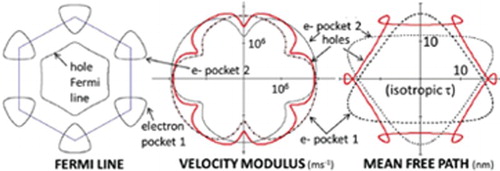
Given the high ρc/ρab ratios obtained, Ouisse et al. [Citation1] applied a simple 2D, near free electron, NFE, model to a hexagonal metal, with the same lattice parameters as Ti2AlC. The logic being that if one is to understand the 3D nature of conductivity in these materials, it behooves us to understand their 2D conductivity first. Figure (b) plots the projection, unto the basal plane, of Ti2AlC, FS (Figure (a)), obtained from DFT calculations (all colors but red), along with the fit of the Fermi line given by the nearly free electron 2D model assuming U = 0.35 eV and N = 6, together with an appropriate interplane-induced splitting (red lines). Here, U is the Fourier component of the periodic potential for a wave vector joining the centers of two adjacent Brillouin zones and N is the total number of electrons per unit cell populating all partially filled bands. The excellent agreement between the simple 2D approach (red lines in Figure (b)) and the more involved DFT-based projections suggests that this approach has merit. Armed with this model, one can now plot the Fermi lines (Figure (c)), radial plot of the velocity (Figure (d)) and the mean free path (Figure (e)), assuming, N = 6, hole and electron scattering times being respectively, τp = τn = 10−14 s, U = 0.75 eV, a = 0.304 nm, c = 1.36 nm and four 2D M-planes per unit cell (bottom unit cell in Figure (a)). This simple model is able to explain a number of observations outlined in the introduction, as well as others that did not make much sense in an isotropic two-band model.
Figure 2. (a) DFT Fermi surface of Ti2AlC, (b) projection of FS on basal plane (in color) and simple 2D Fermi lines assuming a simple NFE 2D model (in red). (c) 2D Fermi lines and corresponding, (d) velocity modulus and (e) mean free paths [Citation1]. Applied magnetic field B is into the page.
![Figure 2. (a) DFT Fermi surface of Ti2AlC, (b) projection of FS on basal plane (in color) and simple 2D Fermi lines assuming a simple NFE 2D model (in red). (c) 2D Fermi lines and corresponding, (d) velocity modulus and (e) mean free paths [Citation1]. Applied magnetic field B is into the page.](/cms/asset/b9d14739-841c-4980-83b1-f845861cf315/tmrl_a_1333537_f0002_c.jpg)
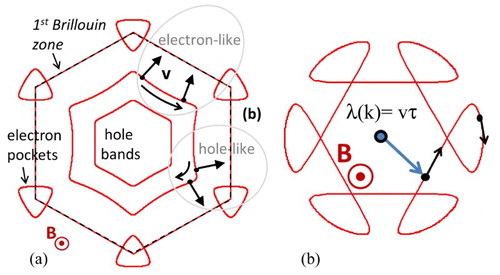
To understand the implications and ramifications of this 2D model, we start by noting that the hole FSs form open tubes, further justifying our 2D model, and allowing us to use the hole and electron Fermi lines given by that model (Figure (a)). The Boltzmann equation—at low B, and assuming a relaxation time approach is valid—for conventional metals is given by
(1)
where Δf is the out-of-equilibrium part of the carrier distribution function, f,
is the electric field, v is the velocity, τ is the relaxation time and
is the reduced Plank’s constant. Using Equation (1), the transport properties can be easily solved for by taking into account either the local curvature of the Fermi line or a variation of τ along it [Citation1].
Figure 3. (a) Effect of Fermi line curvature on response of holes to B, applied along the c-axis of the hexagonal crystal. In some directions, the holes rotate clockwise and in others counterclockwise. (b) Mean free path, λ, of holes from (a). The net effect is determined by subtracting the areas of the outer loops from the area of the inner hexagon.
Analysis of basal plane transport is also made easier by using well-established theoretical results, and aid in understanding why the parameters extracted from a simple one- or two-carrier analysis bring about figures with no connection with the real electron and hole densities. In particular, the transverse 2D conductivity, in weak B field limit, is given by [Citation29]
(2)
where Ai is the oriented area spanned by the mean free path, λ, when the wavevector, k, cycles over one cyclotron orbit around the Fermi line. It shows that the transverse 2D conductivity only depends on λ, which is the product of v and τ. Note that λ, v and τ may all possibly vary with k. Furthermore, the combination of several bands leads to an overall ρab and RH of the form [Citation29]:
(3)
(4)
Combining Equations (2) and (3), it is clear that a hole band and an electron band—with similar scattering processes—will tend to cancel the Hall coefficient, independent of their carrier density ratios (a case likely to apply if those bands are created from the splitting of a free Fermi line at the BZ boundaries in an NFE model). This simple consideration clearly shows that a vanishing RH does not necessarily imply compensation by equal numbers of electrons and holes with similar mobilities.
Complexity does not end here, however, because even a single band can give rise to apparent compensated transport. Consider a hole band, as depicted in Figure (b), somewhat mimicking the hole Fermi line of Ti2AlC (Figure (b)). Holes rotate along the Fermi line according to the semi-classical law of motion ħ∂k/∂t = ev × B. At a given k value, v is perpendicular to the tangent of the Fermi line. If the curvature of the Fermi line changes sign, then the rotation of the velocity with time can switch from clockwise to anticlockwise, so that positively charged holes can rotate either clockwise or anticlockwise in real space (Figure (a)). This leads in turn to apparent compensation, manifest in the apparition of negatively oriented, outer flaps in the radial plot of λ, and to a corresponding decrease in RH.
It also leads to the existence of an MR, even though one is dealing with a single band. Although not widely appreciated, such a phenomenon prevails in many metals [Citation29,Citation30] and is discussed in detail in [Citation1] in the context of MAX phases. Owing to the predicted complexity of the latter, this makes the experimental determination of carrier densities from magnetotransport measurements problematic.
Starting with the 2D model shown in Figure (b) and assuming the existence of several bands the computations in [Citation1] explain the following:
Why napp ≈ papp ≈ 1027 m−3, despite the fact that the actual values of n and p can be quite different. A single-band model would give only holes with papp ≈ 4.6 × 1028 m−3, while the actual values derived from the 2D model in this case are p = 2 × 1028 and n = 2 × 1027 m−3.
Why an MR signature exists in the first place.
Why RH is typically small in many MAX phases. This is attributed to the fact that RH is not only determined by n and p (p in this case), but also by the local curvature of the Fermi lines (Figure (a)). As the holes move along the basal planes in some directions, they are deflected by the magnetic field as electrons and in others as holes, namely clockwise and anticlockwise.
Why RH sometimes changes sign. In the 2D model presented above, it was assumed that τp = τn =10−14 s. However, if that ratio is changed slightly—say with T changes, a not unreasonable assumption given the anisotropies in atomic displacement parameter [Citation31] (see below) —then RH can actually change sign as has sometimes been observed [Citation18].
Why napp and papp are sometimes found to be a function of T [Citation15]. As noted above, this observation cannot be easily reconciled with a conventional two-band model, for which metallic charge carrier densities are not expected to noticeably vary with T.
Based on these considerations, a fruitful approach to understanding transport in the MAX phases is to attempt to reproduce Figure for a number of other MAX phases using as few parameters as possible. Once that is established, a 2D analysis—as carried out here for Ti2AlC—should be carried out in order to match experiment and theory. This approach should work better for smaller, rather than larger, values of N. It should thus work reasonably well for Ti, Zr and, possibly, Hf-based MAX phases. Lastly, we note that this 2D model is also an excellent place to start to try and understand transport in MXenes (see below) that are by nature 2D.
2.2. Real Fermi surfaces
We now proceed from Fermi lines to Fermi surfaces, FSs. Figure plots a number of MAX phases’ FSs. The FSs are quite complicated and, at first glance, appear to be quite different. However, within the variability, there are some commonalities and differences:
The FS shapes are determined more by the M elements than the A elements. This best seen by comparing the FSs of group 4 elements, Ti, Zr, Hf (Figure (a)–(c)) to those of group 5 elements, V and Nb (Figure (e,f)). The former are more similar to each other than they are to the latter. The FS of Mo2GaC (group 6) is quite different from all others (Figure (g)).
The FSs of the Ti-containing 211 phases are quite comparable. This is best seen by comparing the FS of Ti2AlC (Figure (a)) to that of Ti2SnC (Figure (a)).
The FS of Ti2AlC (Figure (a)), Ti3AlC2 (Figure (d)) and Ti3SiC2 (Figure (h)) share similarities. Note the difference between the latter two is in the value of N; it is one greater in Ti3SiC2. It is quite possible that Ti2SnC, Ti3AlC2 and Ti3SiC2 can be modeled in the same way as Ti2AlC [Citation1].
Figure 4. Fermi surfaces of, (a) Ti2SnC [Citation32], (b) Zr2SnC [Citation33], (c) Hf2SnC [Citation32], (d) Ti3AlC2 [Citation23], (e) V2GaC [Citation34], (f) Nb2GaC [Citation34], (g) Mo2GaC [Citation34] and (h) Ti3SiC2 [Citation23].
![Figure 4. Fermi surfaces of, (a) Ti2SnC [Citation32], (b) Zr2SnC [Citation33], (c) Hf2SnC [Citation32], (d) Ti3AlC2 [Citation23], (e) V2GaC [Citation34], (f) Nb2GaC [Citation34], (g) Mo2GaC [Citation34] and (h) Ti3SiC2 [Citation23].](/cms/asset/8390b7c7-9d2f-4738-a9b6-ca002708614a/tmrl_a_1333537_f0004_c.jpg)
None of these conclusions are too surprising since it has long been established that the DOS at Ef was dominated by the d–d orbitals of the M elements.
In particular, MAX phases are predicted to possess hole bands whose FS often adopts the shape of a bulged open tube along the c-axis, reminiscent of the spatial confinement into planes perpendicular to this direction [Citation22,Citation23,Citation25,Citation35]. Bulges and tube distortions can be very complicated, and the FSs of the various bands are often nested into one another (Figure ). Electron bands are also found in most compounds, sometimes in the form of open tubes as for the holes, and sometimes exhibiting closed surfaces, thereby indicating delocalization along the c-axis [Citation22,Citation23,Citation25]. Furthermore, not all MAX phases’ FSs exhibit the same shape, even if there is a tendency to obtain Γ-centered nested hole tubes, with electron closed surfaces or open tubes centered at the K points. In other words, FSs that are not unlike those of our simple NFE approach. Interestingly, Cr2AlC appears to be an exception in that Γ-centered nested electron tubes are surrounded by hole pockets centered at the M points [Citation36].
Additional band splitting is due to topological differences between the various planes containing the transition metal atoms. However, not all phases are predicted to fit into this scheme [Citation23,Citation35], so that this should not be generalized. If we follow the predictions of the FS, then electrical transport should occur by both electrons and holes, with strong anisotropies lying either in the curvature of the FS or in the relaxation times, along with complications arising from the intricate contribution of a large number of occupied bands to the magnetotransport coefficients, or by anisotropies in the electron–phonon coupling. As discussed in the following sections, it is quite improbable that the electrical transport is dominated by any of these phenomena solely. Most probably, magnetotransport is determined by the overall contribution of various electrons and hole bands, by the anisotropies of the FSs and, in the phonon-limited regime, by anisotropies in electron–phonon coupling. Said otherwise, and as much as it would be desirable, it is unlikely that one transport model will explain transport in all MAX phases. The 2D model, however, should always be considered first before more sophisticated models are adopted.
2.3. Conduction in the c-direction and interplanar defects
Up to this point, the discussion was focused on transport in the basal planes. To shed light on the ρc/ρab ratios, it is instructive to recap what is known about two other well-known layered solids: oriented pyrolytic graphite and high Tc cuprates. In hole-doped cuprates, measured ρc/ρab ratios in the normal state can exceed 105 [Citation37]; ratios for electron-doped cuprates vary from 103 to 104 [Citation38]. In some graphite single crystals, ρc/ρab exceeds 104 [Citation39] and the intrinsic value is indeed still unknown. For pyrolytic graphite, ρc/ρab varies from 10 to 3000, and depends almost exponentially on the deposition temperature [Citation39]. This dependence is an important and crucial clue since it strongly suggests that interlayer defects are responsible for the out-of-plane conductivity (Figure (a)) and can result in MR. Indeed, this is the understanding to date. And since there is no reason to believe the situation is different herein we tentatively make the same conclusion. One needs to emphasize once again that the DOS of the A and X elements at EF are quite small, sometimes vanishingly so.
Figure 5. (a) Schematic showing how an imperfect 2D conducting material can nevertheless result in a current along the c-axis and give rise to an MR. (b) FS of Nb2GeC [Citation40].
![Figure 5. (a) Schematic showing how an imperfect 2D conducting material can nevertheless result in a current along the c-axis and give rise to an MR. (b) FS of Nb2GeC [Citation40].](/cms/asset/b79da6a8-18ef-44b8-9135-6c0d0512d449/tmrl_a_1333537_f0005_c.jpg)
It follows that the ρc/ρab ratio can be used as an indirect measure of a single crystal/thin film’s quality. In this, it is not unlike the idea that the RRR is also a measure of a sample’s quality. We thus predict that as more perfect single crystals are produced, the ρc/ρab ratio will increase accordingly. And while it is always dangerous to generalize based on a limited—two in this case—data set, the similarities in the nature of DOS at EF for most MAX phases suggest that the intrinsic ρc/ρab ratio for most of them will be quite high. These comments notwithstanding, that does not necessarily mean it will be the case for all MAX phases. When the resistivity results obtained on a Ti2GeC epitaxial thin film of high quality (with an RRR of ≈ 25) were compared to bulk properties of the same composition the anisotropy ratio—at ≈1.6—was found to be quite mild [Citation20]. Interestingly, the FS of Nb2GeC (Figure (b)) also suggests that this compound would act more like a 3D than a 2D conductor [Citation40].
Quasi-2D systems usually exhibit unusual properties, mostly due to the correlations ruling the electron interactions that sometimes result in outstanding phenomena, ranging from high TC superconductivity [Citation38], to non-Fermi liquid properties [Citation41]. Although all existing data indicate a strong electron–phonon coupling, the MAX phases are indeed not ‘good’ superconductors, with only a few phases exhibiting superconductivity at quite low T’s [Citation15]. However, some recently engineered MAX phases exhibit magnetic properties [Citation42–45]. The impact of this magnetism on transport has just started to be assessed [Citation46], and should bring interesting developments in the near future. More generally, correlations often result in departures from Fermi liquid theory [Citation47,Citation48], and to assess whether this is the case for the MAX phases remains to be explored. Although the MAX phases are neither outstanding superconductors nor intriguing topological insulators, this point is nevertheless worth being investigated.
2.4. Kohler’s rule
Returning to the Boltzmann equation (Equation (1)) roughly speaking, since the term in brackets can be expanded as a function of Bτ, and no other term depends on B, this implies that any transport property should be a function of Bτ, and in turn on B/ρ. This is known as Kohler’s rule (a more rigorous derivation where Kohler’s rule is derived in tensor form can be found in [Citation49]).
If Equation (1) is valid, then for a conventional Fermi liquid, plots of MR vs. B/ρ0—or more usually Δρ/ρ0 vs. (B/ρ0)2 should be independent of T [Citation49]. Said otherwise, if Kohler’s rule is upheld, then the material can be considered a conventional Fermi liquid [Citation49], as indeed observed for V2AlC single crystals (Figure (a)) and preliminary results for Ti3SiC2 (not shown). In contradistinction, the same cannot be said about Cr2AlC single crystals. With data taken from Ref. [Citation1], it is clear that Cr2AlC not only does not obey Kohler’s rule (Figure (b)). In this case, the scaling law is wherein MR is proportional to the Hall angle, namely (θH)2 viz. (RHB/ρ0)2 is independent of T (Figure (c)). This response is thus similar to exotic, quasi-2D systems [Citation50–52] such as high TC superconducting cuprates [Citation50], heavy Fermion compounds [Citation51], or Fe superconducting pnictides in their normal state [Citation52]. The explanations for the latter observation have been diverse: from non-Fermi liquid theories [Citation48], local variations of the Hall angle on the Fermi line induced by antiferromagnetic interactions prevailing in localized parts of the Fermi line [Citation47], to variations in carrier density with T, which is unlikely for quasi-2D metals with appreciable carrier densities, but yet advocated by some [Citation53,Citation54].
Figure 6. Effect of temperature on transverse magnetoresistance, MR, when plotted for single crystals of (a) V2AlC; MR vs. (B/ρ0)2, (b) Cr2AlC; MR vs. (B/ρ0)2 and (c) Cr2AlC; MR vs. (RHB/ρ0)2. Data taken from [Citation1]. Each color line represents a different temperature.
![Figure 6. Effect of temperature on transverse magnetoresistance, MR, when plotted for single crystals of (a) V2AlC; MR vs. (B/ρ0)2, (b) Cr2AlC; MR vs. (B/ρ0)2 and (c) Cr2AlC; MR vs. (RHB/ρ0)2. Data taken from [Citation1]. Each color line represents a different temperature.](/cms/asset/fb952954-3d87-4790-aceb-7ceeeb05644c/tmrl_a_1333537_f0006_c.jpg)
Identification of the physical mechanism leading to this scaling law should certainly be the subject of future research, for it might not only shed light on MAX phases, but also on other quasi-2D systems, where the controversy is still open, sometimes after decades of debate [Citation49]. Cr2AlC exhibits a higher thermal expansion coefficient than most other MAX phases [Citation15], a larger electron–phonon coupling constant [Citation15], and is predicted to be antiferromagnetic [Citation55]. Whether any of those three properties plays a role has yet to be established.
The conventional two-band isotropic model with napp ≅ papp is the simplest one can imagine to explain the existence of a MR, leading to an MR: Δρ/ρ0 = µnµpB2, and ρ0 the resistivity for B = 0. Along with a simple one-band model, it is also currently the only tractable model for parameter extraction. However, it is worth recalling that any distortion in a spherical Fermi sphere must also give rise to an MR. As noted above, the complexity of the predicted FSs makes it highly doubtful the physical reality of the extracted carrier densities. The point is that not only several bands come into play, but that each band, considered alone, and as explained above, could give rise to an MR and vanishingly small RH values.
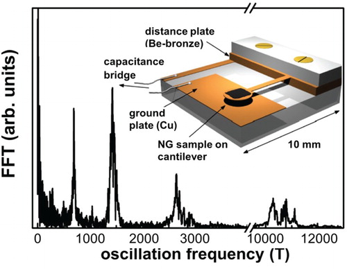
Although no experimentally acquired FS landscape of any MAX phase can be found in the literature, preliminary data measured at LNCMI, Grenoble, definitely prove its complexity. As seen in Figure , measurements of de Haas van Alphen quantum oscillations of the magnetization with B in single-crystalline Ti3SiC2 clearly indicate the existence of multiple frequencies, and thus the contribution of many extremal orbits, a fact incompatible with the existence of two similar, isotropic electron and hole bands (the latter should give rise to a single frequency, independent of orientation of B). A better formulation of the carrier density problem would be: Why are the apparent electron and hole densities more or less equal in most MAX phases?
Figure 7. Frequency spectrum of the quantum de Haas van Alphen oscillations of the magnetization of a single crystal of Ti3SiC2 measured at T = 1.3 K. Here the applied magnetic field B is parallel to the c-axis (by courtesy of B. Piot, LNCMI, Grenoble).
3. MXenes
Work on trying to understand transport in the MAX phases is roughly 20 years old and as shown herein more is still unknown than known. Their 2D counterparts—generated by etching the A layers from the MAX phases [Citation6,Citation7] —are only 5 years old and thus even much less is known about them. And while there is no doubt that magnetotransport in MXenes is more two dimensional than their parent phases, understanding it is probably even more challenging for several reasons, chief among them are: (i) when the A layers are etched, they are replaced by O, F and OH terminations (Figure (a)) [Citation6,Citation7,Citation56]. (ii) In most cases, the interlayer space is populated by cations and water molecules [Citation57], the exact arrangement of which is unknown. (iii) The exact stacking in multilayered particles can vary from particle to particle or from batch to batch. (iv) The possible presence of a large fraction of defects in the 2D sheets, especially when aggressive etchants such as 50% HF are used. In solids, in general and 2D solids in particular it is difficult to characterize and quantify point defects.
There have been few fundamental experimental transport studies on MXenes. The existing transport studies come in two flavors, those carried out on pressed MXene discs or thick films made by filtration. It is difficult to say anything about the fundamentals of transport from these studies since the control on flake-to-flake contact, arrangement, etc. is difficult to reproduce, let alone characterize. The most that can be extracted from such studies is the slope of ρ vs. T plots. For the most part, the slopes are positive, consistent with the metallic nature of MXenes. In some cases, the slopes are negative, which prompted some to claim semiconductor-like characteristics [Citation58–60]. However, since the negative slopes are most probably a result of a large number of defects, such a description may be misleading.
Plots of ρ vs. T can also be used to shed light on the transport mechanisms. For example, we showed that in the T range between 10 and 60 K, the T dependence of the conduction in Ti3C2Tx, in the form of etched epitaxial thin films [Citation61], was compatible with a 2D variable range hopping mechanism. Interestingly, the MRs for these films were negative. In contrast, the MRs in Mo2C [Citation59] and Mo2TiC2Tx [Citation60] films were positive.
The other set of measurements, carried out mostly on Ti3C2Tx, in the form of epitaxial thin films [Citation61], spin-coated films [Citation62], single flakes [Citation63,Citation64] and individual multilayered particles, are more useful for shedding light on the transport problem because the arrangement of the flakes in these incarnations is more uniform. Figure plots the carrier densities as a function of temperature for epitaxial thin films [Citation61]. Top inset plots the Hall resistance, RH, vs. applied magnetic field, lower inset plots ρab vs. B both up to 9 T.
Figure 8. Charge carrier densities vs. T for etched, epitaxial Ti3C2Tx thin films [Citation61]. Top inset plots the Hall resistance, RH, vs. applied magnetic field H up to 9 T. Lower inset plots ρab vs. H up to 9 T. Note negative MR. (Results courtesy J. Halim, C. Smith and S. May, Drexel University, Philadelphia, PA).
![Figure 8. Charge carrier densities vs. T for etched, epitaxial Ti3C2Tx thin films [Citation61]. Top inset plots the Hall resistance, RH, vs. applied magnetic field H up to 9 T. Lower inset plots ρab vs. H up to 9 T. Note negative MR. (Results courtesy J. Halim, C. Smith and S. May, Drexel University, Philadelphia, PA).](/cms/asset/23ffbddd-5f1b-46c2-8194-b3245a26ead4/tmrl_a_1333537_f0008_c.jpg)
Results such as those shown in Figure can—assuming a single-band model—be used to calculate the density of carriers and their mobilities. These values extracted from five such studies are summarized in Table . In one case, the conductivities of Ti3C2Tx multilayers and Ti3C2Tx particles were measured along, and normal to, the basal planes [Citation67]. The reported anisotropy was about an order of magnitude between the in- and out-of-plane conductivities. However, at 24 and 1.4 S/cm, the conductivities were orders of magnitude lower compared to the rest of the values listed in Table . Similarly, the results of Lai et al. [Citation65] —who report mobilities of 10,000 cm2/Vs and carrier densities that are more than one order of magnitude lower than other reports (Table ) —are clear outliers. These two studies are thus not included in what follows.
Table 1. Summary of room temperature conductivities, apparent carrier densities and mobilities, µ, for Ti3C2Tx.
For reasons that are not quite clear, the carrier densities—again assuming a single-band model—measured, 3–5 × 10²² m−3, on spincast [Citation62] and epitaxial [Citation61] films are higher than the single flake values (Table ). In the first measurement ever on a single Ti3C2Tx flake, the carrier density was reported to be 8 ± 3 × 1014 cm−2 [Citation63]. A slightly higher value of 1 ± 0.3 × 1015 cm−2 was later reported by others [Citation64]. Taken in toto, it is reasonable to conclude that the carrier density in Ti3C2Tx is more or less fixed at ≈1 × 1015 cm−2 or—assuming a thickness of 1 nm—1 × 1022 cm−3. This is an important conclusion and suggests that this value is intrinsic to this MXene. Note, however, that this value is also an apparent value assuming a single-band model. The leitmotiv of this paper is that such values are at best effective values. To get the true values requires detailed knowledge of the FSs or lines in this case. Not surprisingly, the carrier mobilities, on the other hand, depend on flake quality and range between ≈0.2 and ≈3 cm2/Vs [Citation62–64].
Miranda et al. [Citation63] were also the first to show that at room temperature it was not possible to modulate the drain-source currents using gate modulation, a not too surprising result given the metal-like density of carriers (Table ) [Citation63]. Here again, this was later confirmed by others [Citation64]. Miranda et al. [Citation63] did, however, see a change in mobilities at 2.5 K that they ascribed preliminarily to the complexities of the FS.
Interestingly, when the conductivities of Ti3C2Tx single flakes and films made of the same flakes are compared, the difference is about an order of magnitude lower for the latter, implying that flake-to-flake electron transport—that has to go through the surface terminations—is surprisingly good [Citation62,Citation64]. From an application point of view, this is an important aspect that needs to be better understood. For example, one potential application for MXenes is as transparent conductive electrodes [Citation62,Citation68]. A good figure of merit, FOM, is the ratio of DC conductivity to an optical conductivity, or σdc/σop [Citation69]. As shown in Table , films spin-coated from aqueous colloidal MXene solutions have the highest FOMs for this application. Note that the FOM of Ti2CTx [Citation68] and Ti3C2Tx [Citation62] spin-coated films is comparable to those of chemically vapor deposited un-doped graphene [Citation69]. Based on the current results, and when normalized per Ti atom, the spin-coated Ti2CTx films have to be considered the best [Citation68].
Table 2. Summary of optoelectronic properties of MXene films.
In contrast to the relative paucity of experimental papers, there have been a larger number of DFT papers, dealing with the electronic structure of MXenes, especially as a function of termination chemistries [Citation6,Citation67,Citation73–77]. In the remainder of this section, we summarize the consensus from these calculations. They are:
The MAX to MXene transformation in Ti3C2Tx and Ti2CTx should result in an increase in the DOS at EF.
Bare MXenes—with no terminations—should be metallic.
In the first report on Ti3C2Tx [Citation6], a small gap of 0.05 eV was predicted if it were OH-terminated and a 0.1 eV gap if it were F-terminated. And while these predictions have since been confirmed by others [Citation78], as noted above, there is scant experimental evidence to back them up.
One may argue that such band gaps are small and could be missed experimentally. However, others have predicted large band gaps for O-terminated MXenes. For example, Khazaei et al. ([Citation73,Citation79]) predicted the following band gaps: 0.24 eV for Ti2CO2 and 0.88 eV for Zr2CO2 and 1 eV for Hf2CO2. Here, again these predictions await experimental verification.
Interestingly, the F, OH or O terminations introduce new bands—comprised mainly of p-orbitals—close to the M d bands. Two outcomes can be envisioned, as thoroughly described in a recent review paper by Khazaei et al. [Citation79]. First, if hybridization of these new bands with the M d orbitals remains weak around EF (e.g. with OH groups), then the main effect of the functionalization is to induce an electron transfer between the T’s and the M’s, and thus simply sweep the Fermi level through a d-band structure left roughly unmodified around EF. In that case, a slight modification of the nature of the functionalization or of the stacking of the layers can result in substantial modification to the Fermi surface. A good example can be seen for the only published FS of an MXene, that of Ti3C2Tx [Citation67]. In this work, the authors examined a single flake (Figure (b)) and two stacking configurations: Bernal and simple hexagonal shown in Figure (c,d), respectively. Not surprisingly, dispersion along the c-axis was quite small confirming a 2D electronic structure. Interestingly, the FS is the reverse of the parent MAX phase (Figure (d)) in that the electrons are now in the center, with hole pockets around the edges.
Figure 9. (a) Schematic of Mn + 1CnTx MXene showing OH, O and F terminations. (b) FS of a Ti3C2(OH)2 monolayer. FS of multilayers assuming the MX-block stacking in (a) is, (c) Bernal or, (d) simple hexagonal [Citation67].
![Figure 9. (a) Schematic of Mn + 1CnTx MXene showing OH, O and F terminations. (b) FS of a Ti3C2(OH)2 monolayer. FS of multilayers assuming the MX-block stacking in (a) is, (c) Bernal or, (d) simple hexagonal [Citation67].](/cms/asset/fe02c77a-0f04-4a45-830a-5d6a786192b2/tmrl_a_1333537_f0009_c.jpg)
Remarkably, sweeping EF through an unmodified d-band can readily reproduce these results. To show this, in Figure , we plot the Fermi lines obtained by diagonalizing a simple and easy-to-solve tight-binding Hamiltonian involving only the M d and C p and s orbitals (M2C phase, 14 × 14 Hamiltonian, parameters that are close to those given in [Citation80]). Figure (a–c) is obtained by sweeping down EF through rigid bands over intervals of the order of 20 meV. As rough as this model is, the similarity between these results and those obtained by DFT (Figure ) is striking.
Figure 10. Fermi lines of termination-free 2D Ti2C obtained from a simple tight-binding model using Harrison’s parameters [Citation80] and including only the M d and the C s and p orbitals. In going from left to right, EF is shifted downwards by ≈20 meV each time. The similarities with the results shown in Figure (b,c) are striking.
![Figure 10. Fermi lines of termination-free 2D Ti2C obtained from a simple tight-binding model using Harrison’s parameters [Citation80] and including only the M d and the C s and p orbitals. In going from left to right, EF is shifted downwards by ≈20 meV each time. The similarities with the results shown in Figure 9(b,c) are striking.](/cms/asset/694d87df-ebb4-476e-9cbb-a25b3c2a825c/tmrl_a_1333537_f0010_c.jpg)
As noted in Khazaei et al. [Citation79], the second main effect occurs when the hybridization between the p T and C p or M d orbitals becomes more substantial. Then, not only is the band structure appreciably modified, even in the vicinity of the original Fermi-level position in the pristine MXene, but the Fermi-level shift is predicted to become large enough so as to drive EF in the forbidden gap separating the d bands from the hybridized p T and C p bands. If these predictions are verified, then they would in turn render MXenes direct competitors to the semiconducting members of the transition metal di-chalcogenide family.
An interesting magnetotransport feature that has been observed for various MXenes has been a negative MR [Citation61]. In addition, observation of a dependence of the conductivity with temperature T proportional to exp(−(T0/T)1/3) in the low T regime strongly suggests that variable range hopping is operative [Citation59,Citation61]. Such a mechanism in turn suggests that we are dealing with, (i) a heavily doped semiconductor, (ii) a highly disordered metallic phase exhibiting a mobility edge or (iii) granular metals where the energy barriers are formed in between the metal grains. At this time, the published results do not allow us to discriminate between those possibilities. Higher T measurements could indicate the presence of an activated regime in the resistivity with an activation energy corresponding to the depth of the impurity band in the band gap, or to the mobility edge of a highly disordered metal. Gated devices fabricated with these phases should also allow one to definitely demonstrate or refute their semiconducting nature.
4. Perspectives and final thoughts
As single-crystalline/single flake transport data have only started to be measured there is still much to be done before a thorough picture of the physical mechanisms governing magnetotransport in the MAX phases and MXenes, including the anisotropies, emerges. The high number of existing phases makes the task a hard one, especially given the fact that many phases cannot be easily produced in single crystal form with techniques such as solution growth, due to the poor carbon solubility in liquids containing, e.g. Ga, In or Sn, or in a suitable crystal orientation and with a high enough quality in the case of thin deposited or converted single-crystalline layers. Ironically enough, since it is somewhat easier to deposit MXene single flakes, and measure their transport properties [Citation63,Citation64,Citation81], we may learn more about transport in the MAX phases from their much younger 2D cousins.
To conclude for a better understanding of magnetotransport in the MAX phases, the following experiments—to be carried out on single crystals—are recommended:
Experimentally assess the Fermi surface shapes and how well they conform to those obtained from ab initio calculations. This can be obtained either by deciphering dHvA oscillations in single crystals (in progress at LNCMI, Grenoble, see Figure ) or by a direct measurement using Angle Resolved PhotoEmission Spectroscopy or ARPES (in progress at Nagoya University).
Measurement of thermopower as a function of orientation.
Thorough investigation of magnetotransport properties in magnetic MAX phases.
Assess correlation between anisotropy ratio and crystal quality.
Determine the influence of defects such as vacancies and bulk ripplocations [Citation82] on electronic properties.
Understand why Cr2AlC—and possibly others— exhibits the same scaling law as ‘exotic’ quasi-2D compounds, whereas others, such as V2AlC and Ti3SiC2, do not.
Find a method to isolate electron—phonon coupling anisotropy and measure it.
Find a general explanation for the napp = papp rule, in a way more elegant than relying on numerical integrations of the transport properties along the calculated Fermi lines.
Determine whether all bulk MAX single crystals exhibit high anisotropy resistivity ratios.
Determine whether magnetotransport is affected by magnetic breakdown phenomena, since many bands are predicted to get quite close to each another by ab initio DFT calculations.
Try to discover the elusive MXenes with band gaps and/or magnetic properties.
Acknowledgements
Many thanks are due to B. Piot (LNCMI) for allowing us to use some yet unpublished data (Figure ), and to L. Shi (LMGP and UCL) and B. Hackens (UCL) for their help in treating the magnetotransport data already published in [Citation1].
Disclosure statement
No potential conflict of interest was reported by the authors.
ORCID
Michel Barsoum http://orcid.org/0000-0001-7800-3517
Additional information
Funding
References
- Ouisse T, Shi L, Piot BA, et al. Magnetotransport properties of nearly-free electrons in two-dimensional hexagonal metals and application to the Mn + 1AXn phases. Phys Rev B. 2015;92:045133. doi: 10.1103/PhysRevB.92.045133
- Nowotny H. Strukturchemie Einiger Verbindungen der Ubergangsmetalle mit den elementen C, Si, Ge, Sn. Prog Solid State Chem. 1970;2:27–30. doi: 10.1016/0022-4596(70)90028-9
- Barsoum MW, El-Raghy T. Synthesis and characterization of a remarkable ceramic: Ti3SiC2. J Amer Cer Soc. 1996;79:1953–1956. doi: 10.1111/j.1151-2916.1996.tb08018.x
- Barsoum MW, Brodkin D, El-Raghy T. Layered machinable ceramics for high temperature applications. Scrip Met Mater. 1997;36:535–541. doi: 10.1016/S1359-6462(96)00418-6
- Barsoum MW, Farber L, Levin I, et al. High-resolution transmission electron microscopy of Ti4AlN3, or Ti3Al2N2 revisited. J Amer Cer Soc. 1999;82:2545–2547. doi: 10.1111/j.1151-2916.1999.tb02117.x
- Naguib M, Kurtoglu M, Presser V, et al. Two dimensional nanocrystals produced by exfoliation of Ti3AlC2. Adv Mater. 2011;23:4248–4253. doi: 10.1002/adma.201102306
- Naguib M, Mashtalir O, Carle J, et al. Two-dimensional transition metal carbides. ACS Nano. 2012;6:1322–1331. doi: 10.1021/nn204153h
- Medvedeva N, Novikov D, Ivanovsky A, et al. Electronic properties of Ti3SiC2-based solid solutions. Phys Rev B. 1998;58:16042–16050. doi: 10.1103/PhysRevB.58.16042
- Hug G, Fries E. Full-potential electronic structure of Ti2AlC & Ti2AlN. Phys Rev B. 2002;65:113104. doi: 10.1103/PhysRevB.65.113104
- Ahuja R, Eriksson O, Wils JM, et al. Electronic structure of Ti3SiC2. Appl Phys Lett. 2000;76:2226–2228. doi: 10.1063/1.126304
- Lofland SE, Hettinger JD, Meehan T, et al. Electron-phonon coupling in MAX phase carbides. Phys Rev B. 2006;74:174501. doi: 10.1103/PhysRevB.74.174501
- Drulis MK, Czopnik A, Drulis H, et al. Low temperature heat capacity and magnetic susceptibility of Ti3SiC2. J Appl Phys. 2004;95:128–133. doi: 10.1063/1.1631077
- Drulis MK, Czopnik A, Drulis H, et al. On the heat capacities of Ti3GeC2. Mater Sci Eng B. 2005;119:159–163. doi: 10.1016/j.mseb.2005.02.045
- Drulis MK, Drulis H, Gupta S, et al. On the heat capacities of M2AlC (M = Ti, V, Cr) ternary carbides. J Appl Phys. 2006;99:093502. doi: 10.1063/1.2191744
- Barsoum MW. MAX phases: properties of machinable carbides and nitrides. Weinheim: Wiley VCH GmbH; 2013.
- Yoo HI, Barsoum MW, El-Raghy T. Ti3SiC2: a material with negligible thermopower over an extended temperature range. Nature. 2000;407:581–582. doi: 10.1038/35036686
- Finkel P, Hettinger JD, Lofland SE, et al. Magnetotransport properties of the ternary carbide Ti3SiC2: hall effect, magnetoresistance and magnetic susceptibility. Phys Rev B. 2001;65:035113. doi: 10.1103/PhysRevB.65.035113
- Finkel P, Barsoum MW, Hettinger JD, et al. Low-temperature transport properties of nanolaminates Ti3AlC2 and Ti4AlN3. Phys Rev B. 2003;67:235108. doi: 10.1103/PhysRevB.67.235108
- Hettinger JD, Lofland SE, Finkel P, et al. Electrical transpot, thermal transport and elastic properties of M2AlC (M = Ti, Cr, Nb and V) phases. Phys Rev B. 2005;72:115120. doi: 10.1103/PhysRevB.72.115120
- Scabarozi TH, Eklund P, Emmerlich J, et al. Weak electronic anisotropy in the layered nanolaminate Ti2GeC. Solid State Commun. 2008;146:498–501. doi: 10.1016/j.ssc.2008.03.026
- Zhou YC, Dong HY, Wang XH, et al. Electronic structure of the layered ternary carbides Ti2SnC and Ti2GeC. J Phys: Condens Matter. 2000;12:9617–9627.
- Chaput L, Hug G, Pecheur P, et al. Ansiotropy and thermopower is Ti3SiC2. Phys Rev B. 2005;71:121104(R). doi: 10.1103/PhysRevB.71.121104
- Chaput L, Hug G, Pecheur P, et al. Thermopower of the 312 MAX phases Ti3SiC2, Ti3GeC2, and Ti3AlC2. Phys Rev B. 2007;75:035107. doi: 10.1103/PhysRevB.75.035107
- Magnuson M, Mattesini M, Van Nong N, et al. The electronic-structure origin of the anisotropic thermopower of nanolaminated Ti3SiC2 determined by polarized X-ray spectroscopy. Phys Rev B. 2012;85:195134. doi: 10.1103/PhysRevB.85.195134
- Mauchamp V, Yu W, Gence L, et al. Anisotropy of the resistivity and charge-carrier sign in nanolaminated Ti2AlC: experiment and ab initio calculations. Phys Rev B. 2013;87:235105. doi: 10.1103/PhysRevB.87.235105
- Ouisse T, Sarigiannidou E, Chaix-Pluchery O, et al. High temperature solution growth and characterization of Cr2AlC single crystals. J Crystal Growth. 2013;384:88–95. doi: 10.1016/j.jcrysgro.2013.09.021
- Shi L, Ouisse T, Sarigiannidou E, et al. Synthesis of single crystals of V2AlC phase by high-temperature solution growth and slow cooling technique. Acta Mater. 2015;83:304–309. doi: 10.1016/j.actamat.2014.10.018
- Mercier F, Chaix-Pluchery O, Ouisse T, et al. Raman scattering from Ti3SiC2 single crystals. Appl Phys Letters. 2011;98:081912. doi: 10.1063/1.3558919
- Ong NP. Geometric interpretation of the weak-field Hall conductivity in two-dimensional metals with arbitrary Fermi surface. Phys Rev B. 1991;43:193–201. doi: 10.1103/PhysRevB.43.193
- Banik NC, Overhauser AW. Hall coefficient of a holelike Fermi surface. Phys Rev B. 1978;18:1521–1532. doi: 10.1103/PhysRevB.18.1521
- Lane NJ, Vogel S, Caspi E, et al. High-temperature neutron diffraction study of Ti2AlC, Ti3AlC2 and Ti5Al2C3. J Appl Phys. 2013;113:183519. doi: 10.1063/1.4803700
- Kanoun MB, Goumri-Said S, Reshak AH. Theoretical study of mechanical, electronic, chemical bonding and optical properties of Ti2SnC, Zr2SnC, Hf2SnC and Nb2SnC. Comp Mater Sci. 2009;47:491–500. doi: 10.1016/j.commatsci.2009.09.015
- Kanoun MB, Goumri-Said S, Reshak AH, et al. Electro-structural correlations, elastic and optical properties among the nanolaminated ternary carbides Zr2AC. Solid State Sci. 2010;12:887. doi: 10.1016/j.solidstatesciences.2010.01.035
- Shein IR, Ivanovskii AL. Structural, elastic, electronic properties and Fermi surface for superconducting Mo2GaC in comparison with V2GaC and Nb2GaC from first principles. Physica C. 2010;470:533–537. doi: 10.1016/j.physc.2010.04.010
- Mattesini M, Magnuson M. Electronic correlation effects in the Cr2GeC Mn + 1AXn phase. J Phys Cond Matter. 2013;25:035601. doi: 10.1088/0953-8984/25/3/035601
- Jia G-Z, Yang L-J. Ab initio calculations for properties of Ti2AlN and Cr2AlC. Physica B. 2010;405:4561–4564. doi: 10.1016/j.physb.2010.08.038
- Martin S, Fiory AT, Fleming RM, et al. Temperature-dependence of the resistivity tensor in superconducting BI2Sr2.2Ca0.8Cu2O8 crystals. Phys Rev Lett. 1988;60: 2194. doi: 10.1103/PhysRevLett.60.2194
- Armitage NP, Fournier P, Greene RL. Progress and perspectives on electron-doped cuprates. Rev Mod Phys. 2010;82:2421. doi: 10.1103/RevModPhys.82.2421
- Klein CA. Electrical properties of pyrolytic graphites. Rev Mod Phys. 1962;34:56. doi: 10.1103/RevModPhys.34.56
- Shein IR, Ivanovskii AL. Structural, elastic, and electronic properties of new 211 MAX phase Nb2GeC from first-principles calculations. Physica B. 2013;410:42–48. doi: 10.1016/j.physb.2012.10.036
- Shishido H, Shibauchi T, Yasu K, et al. Tuning the dimensionality of the heavy fermion compound CeIn3. Science. 2010;327:980. doi: 10.1126/science.1183376
- Ingason AS, Dahlqvist M, Rosen J. Magnetic MAX phases from theory and experiments; a review. J Phys Cond Matter. 2016;28:433003. doi: 10.1088/0953-8984/28/43/433003
- Dahlqvist M, Ingason AS, Alling B, et al. Magnetically driven anisotropic structural changes in the atomic laminate Mn2GaC. Phys Rev B. 2016;93:014410. doi: 10.1103/PhysRevB.93.014410
- Liu Z, Waki T, Tabata Y, et al. Mn-doping-induced itinerant-electron ferromagnetism in Cr2GeC. Phys Rev B. 2014;89:054435. doi: 10.1103/PhysRevB.89.054435
- Tao QZ, Hu CF, Lin S, et al. Coexistence of ferromagnetic and a re-entrant cluster glass state in the layered quaternary (Cr1-x,Mnx)2GeC. Mater Res Lett. 2014;2:192–198. doi: 10.1080/21663831.2014.909542
- Lin S, Tong P, Wang BS, et al. Magnetic and electrical/thermal transport properties of Mn-doped Mnn +1AXn phase compounds Cr2-xMnxGaC (0< × < 1). J Appl Phys. 2013;113:053502. doi: 10.1063/1.4789954
- Anderson PW. Hall-effect in the 2-dimensional luttinger liquid. Phys Rev Lett. 1991;67:2092. doi: 10.1103/PhysRevLett.67.2092
- Kontani H. Anomalous transport phenomena in Fermi liquids with strong magnetic fluctuations. Rep Prog Phys. 2008;71:026501. doi: 10.1088/0034-4885/71/2/026501
- Luo N, Miley GH. Kohler’s rule and relaxation rates in high-T-c superconductors. Physica C. 2002;371:259. doi: 10.1016/S0921-4534(01)01101-7
- Harris M, Yan FY, Matl P, et al. Violation of Kohler’s rule in the normal state magnetoresistance of YBau3O7-δ and La2SrxCuO4. Phys Rev Lett. 1995;75:1391. doi: 10.1103/PhysRevLett.75.1391
- Nakajima Y, Shishido H, Nakai H, et al. Non-Fermi liquid behavior in the magnetotransport of CeMln5 (M: Co and Rh): striking similarity between quasi two-dimensional heavy fermion and high-T-c cuprates. J Phys Soc Japan. 2007;76:024703. doi: 10.1143/JPSJ.76.024703
- Kasahara S, Shibauchi T, Hashimoto K, et al. Evolution from non-Fermi- to Fermi-liquid transport via isovalent doping in BaFe2(As1-xPx)2 superconductors. Phys Rev B. 2010;81:184519. doi: 10.1103/PhysRevB.81.184519
- Ghosh N, Bharathi A, Satya AT, et al. Kohler’s rule in Ba1-xKxFe2As2. Solid State Commun. 2010;150:1940. doi: 10.1016/j.ssc.2010.07.018
- Barišić N, Chan MK, Veit MJ, et al. Hidden Fermi-liquid behavior throughout the phase diagram of the cuprates. arXiv:150707885.
- Dahlqvist M, Alling B, Rosen J. Correlation between magnetic state and bulk modulus of Cr2AlC. J Appl Phys. 2013;113:216103. doi: 10.1063/1.4808239
- Halim J, Cook KM, Naguib M, et al. X-ray photoelectron spectroscopy of Two-dimensional transition metal carbides (MXenes). Appl Surf Sci. 2016;362:406–417. doi: 10.1016/j.apsusc.2015.11.089
- Ghidiu M, Halim J, Kota S, et al. Ion exchange and solvation reactions in 2D Ti3C2 MXene. Chem Mater. 2016;28:3507–3514. doi: 10.1021/acs.chemmater.6b01275
- Anasori B, Xie Y, Beidaghi M, et al. Two-dimensional, ordered, double transition metal carbides (MXenes). ACS Nano. 2015;9:9507–9516. doi: 10.1021/acsnano.5b03591
- Halim J, Kota S, Lukatskaya M, et al. Synthesis and characterization of 2D molybdenum carbide (MXene). Adv Funct Mater. 2016;26:3118–3127. doi: 10.1002/adfm.201505328
- Anasori B, Shi C, Moon EJ, et al. Control of electronic properties of 2D carbides (MXenes) by manipulating their transition metal layers. Nanoscale Horizon. 2016;1:227–234. doi: 10.1039/C5NH00125K
- Halim J, Lukatskaya M, Cook KM, et al. Transparent conductive two-dimensional titanium carbide thin filims. Chem Mater. 2014;26:2374–2381. doi: 10.1021/cm500641a
- Dillon AD, Ghidiu M, Krick A, et al. Highly-conductive, optical-quality films from solution-processed 2D titanium carbide (MXene). Adv Funct Mater. 2016;26:4162–4168. doi: 10.1002/adfm.201600357
- Miranda A, Halim J, Barsoum MW, et al. Electronic properties of freestanding Ti3C2Tx MXene monolayers. App Phys Lett. 2016;108:033102. doi: 10.1063/1.4939971
- Lipatov A, Alhabeb M, Lukatskaya MR, et al. Effect of synthesis on quality, electronic properties and environmental stability of individual monolayer Ti3C2 MXene flakes. Adv Electron Mater. 2016;2:1600255. doi: 10.1002/aelm.201600255
- Lai S, Jeon J, Jang SK, et al. Surface group modification and carrier transport property of layered transition metal carbides (Ti2CTx, T: -OH, -F and –O). Nanoscale. 2015;7:19390–19396. doi: 10.1039/C5NR06513E
- Miranda A, Halim J, Lorke A, et al. Rendering Ti3C2Tx (MXene) monolayers visible. Mater Res Lett. 2017; http://dx.doi.org/10.1080/21663831.2017.1280707.
- Hu T, Zhang H, Wang J, et al. Anisotropic electronic conduction in stacked two-dimensional titanium carbide. Sci Rep. 2015;5:16329. doi: 10.1038/srep16329
- Ying G, Dillon AD, Fafarman AT, et al. Transparent, conductive solution processed spincast 2D Ti2CTx (MXene) films. Mater Res Lett. 2017; doi:10.1080/21663831.2017.1296043
- De S, Coleman JN. Are there fundamental limitations on the sheet resistance and transmittance of thin graphene films? ACS Nano. 2010;4:2713–2720. doi: 10.1021/nn100343f
- Hantanasirisakul K, Zhao MQ, Urbankowski P, et al. Fabrication of Ti3C2Tx MXene transparent thin films with tunable optoelectronic properties. Adv Electron Mater. 2016;2:1600050. doi: 10.1002/aelm.201600050
- Shahzad F, Alhabeb M, Hatter CB, et al. Electromagnetic interference shielding with 2D transition metal carbides (MXenes). Science. 2016;353:1137–1140. doi: 10.1126/science.aag2421
- Mariano M, Mashtalir O, Antonio FQ, et al. Solution-processed titanium carbide MXene films examined as highly transparent conductors. Nanoscale. 2016;8:16371–16378. doi: 10.1039/C6NR03682A
- Khazaei M, Arai M, Sasaki T, et al. Novel electronic and magnetic properties of two-dimensional transition metal carbides and nitrides. Adv Funct Mat. 2013;23:2185–2192. doi: 10.1002/adfm.201202502
- Xie Y, Kent PRC. Hybrid density functional study of structural and electronic properties of functionalized Tin + 1Xn (X = C, N) monolayers. Phys Rev B. 2013;87:235441. doi: 10.1103/PhysRevB.87.235441
- Enyashin AN, Ivanovskii AL. Atomic structure, comparative stability and electronic properties of hydroxylated Ti2C and Ti3C2 nanotubes. Comp Theor Chem. 2012;989:27–32. doi: 10.1016/j.comptc.2012.02.034
- Enyashin AN, Ivanovskii AL. 2D titanium carbonitrides and their hydroxylated derivatives: structural, electronic properties and stability of MXenes Ti3C2-xNx and Ti3C2-xNx(OH)2. J Solid State Chem. 2013;207:42–48. doi: 10.1016/j.jssc.2013.09.010
- Zha XH, Luo K, Li QW, et al. Role of the surface effect on the structural, electronic and mechanical properties of the carbide MXenes. Europhys Lett. 2015;111:6. doi: 10.1209/0295-5075/111/26007
- Tang Q, Zhou Z, Shen P. Are MXenes promising anode materials for Li Ion batteries? Computational studies on electronic properties and Li storage capability of Ti3C2 and Ti3C2X2 (X = F, OH) monolayer. J Amer Chem Soc. 2012;134:16909–16916. doi: 10.1021/ja308463r
- Khazaei M, Ranjbar A, Arai M, et al. Electronic properties and applications of MXenes: a theoretical review. J Mater Chem C. 2017;5:2488. doi: 10.1039/C7TC00140A
- Harrison W. Elementary electronic structure. Singapore: World Scientific; Singapore 2011.
- Sang X, Xie Y, Lin M-W, et al. Atomic defects in monolayer titanium carbide (Ti3C2Tx) MXene. ACS Nano; 2016;10:9193–200.
- Gruber J, Lang A, Griggs J, et al. Evidence for bulk ripplocations in layered solids. Sci Rep. 2016;6:33451. doi: 10.1038/srep33451