
ABSTRACT
We report the fabrication of nickel nanowires with parallel growth-twin structures (‘twin lamella’ along the wire axis) by electrochemical deposition, and demonstrate an interesting twin ‘unzipping’ phenomenon in such nanotwinned nanowires under bending. Through in situ TEM, we found that ‘unzipping’ of twin lamella was achieved by gradually increasing twin spacing along the wire axis via a layer-by-layer twin boundary migration process. Molecular dynamics simulations suggest that partial dislocation slip is responsible for activating the ‘unzipping’, with a multi-step-process involving dislocation loop initiation, expansion and partially annihilation. Our work could provide new insights into the deformation mechanisms of nanotwinned 1-D metallic nanostructures.
GRAPHICAL ABSTRACT
IMPACT STATEMENT
Nickel nanowires with parallel-twin structures were fabricated and demonstrated an interesting twin lamella ‘unzipping’ behavior upon flexural bending, which provides new insights into the deformation mechanisms of nanotwinned metallic materials.
Introduction
One-dimensional (1-D) metallic nanostructures, with extremely high volume/surface ratio, exhibit drastically changed properties with respect to their mechanical, magnetic, electrical and thermal behavior [Citation1–9] when compared to their corresponding bulk system. On the other hand, twin boundaries, as a class of 2-D defects, can strongly influence the mechanical properties of such metallic nanostructures as indicated by earlier simulation works showing that Cu nanowires with tilted twins deform primarily through twin migration by partial dislocation in one active slip system [Citation10]. Under the reversible twinning–detwinning mechanism, superelasticity can be achieved in body-center-cubic (BCC) nanowires [Citation11]. In experiments, the stress required for deformation twinning has a strong crystal size effect [Citation12]. Au nanowires containing angstrom-scaled twins exhibit extremely high tensile strength which reached to their theoretical limit, and the underlying dislocation dynamics and surface nucleation facilitated deformation mechanisms are proved to be twin size dependent [Citation13]. Recently, we discovered that ultrathin Au NW with deformation twins can induce ductile-to-brittle transition [Citation14]. Similar phenomenon had also been observed in Cu nanopillars with orthogonally and slantly orientated twin boundaries [Citation15]. With the rapid development of nanomaterials synthesis and processing techniques, novel nanostructured metals with growth twins have emerged in recent years [Citation16–31] with great interest given that nanotwinned metals exhibit high strength properties coupled with some other modifications such as maintaining the ductility and improvements in electron conductivity [Citation10,Citation11,Citation13–15,Citation17,Citation26,Citation27,Citation32–34]. Such metallic nanostructures with growth twin structures and high strength and high conductivity may also find numerous applications in nanoelectromechanical devices (NEMS), touch panels, field effect transistors (FET) and nano-complementary metal–oxide–semiconductor [Citation35–37]. For these applications, fabrication of nanowires with stable growth nanotwin structures becomes a critical issue. It should be pointed out that nanowire with various twin orientations has been successfully fabricated by electrochemical deposition [Citation38,Citation39]. In this work, we report the successful fabrication of a new type Ni nanowire with unusual twin structures parallel to the wire axis (twin lamella). In addition, an interesting ‘unzipping’ phenomenon of twin lamella has been observed in situ in such nanotwinned nickel nanowires under flexural bending inside transmission electron microscopy (TEM). The deformation mechanism of this intriguing ‘unzipping’ phenomenon observed in parallel-twinned Ni nanowires has also been investigated with the assistance of molecular dynamic (MD) simulation.
Template-assisted electrodeposition of nanotwinned nickel nanowires
Ni nanowires with parallel nanotwins along the wire axis used in this study were fabricated by the typical anodic aluminum oxide (AAO) template-assisted electro-chemical deposition method [Citation40–42]. Driven by the electrical potential, Ni2+ in the deposition solution was transported into the AAO channels and being further reduced into Ni atoms. With the confinement of AAO channels, Ni nanowires were finally formed with diameters determined by the channel diameters [Citation43,Citation44]. By tuning the deposition parameters such as temperature, AAO channel size, DC voltage and magnetic field, etc., these particular Ni nanowires with wire-axis-parallel nanotwin structures were successfully fabricated out (see Figure ). Due to the relatively higher stacking fault energy in Ni (120–130 mJ m−2 [Citation45]) as compared with other face center cubic (FCC) metals like Au, Ag and Cu [Citation46,Citation47], nanotwin structures as reported in previous metallic nanowire synthesis are mostly perpendicular to their wire axis [Citation13,Citation48,Citation49], and such parallel-to-wire-axis nanotwin configurations in Ni nanowires have never been reported so far. Additionally, such nanotwin configurations in nanotwinned Ni nanowires were only observed in nanowires with diameters less than 50 nm, while the twin formation mechanism is still under investigation. Figure (a,b) display our Ni nanowire sample with parallel-to-wire-axis nanotwinned structure under low and high magnifications. The sample is around 390 nm in length and 25 nm in diameter. The twin spacing is around 1 nm. Different from previous studies that mainly focused on the investigation of nanowires with [1 1 1] axial direction [Citation13,Citation15], in this work the wire axial direction is along [−2 1 1]. It is well known that the twin planes in FCC systems are mostly parallel to the most densely packed {111} planes [Citation50,Citation51].
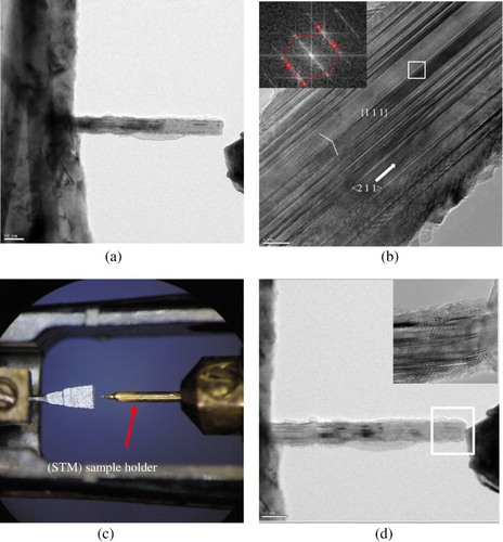
Figure 1. HRTEM images of Ni nanowire under low (a) and high (b) magnifications. Inset shows the diffraction pattern calculated by fast Fourier transform (FFT). Our nanowire has a <2 1 1> axial direction and contains {111} twin boundaries. (c) Experimental setup showing that the nanowire was clamped onto the tip left. (d) TEM images of the mechanical loading of the nanowire. The loading was performed by approaching the tip of STM sample holder to the nanowire. Inset: HRTEM image of the area in white frame. It can be well observed that the deformation consists both bending and compression. Scale bar (a) and (d) 50 nm; (b) 5 nm.
In situ TEM flexural bending experiments
To study the mechanical behavior of nanotwinned metallic structures, in situ TEM methods have been developed and carried out [Citation13,Citation31,Citation52–59] to characterize the underlying deformation mechanisms. In this work, in situ high-resolution TEM (HRTEM) bending experiments of the parallel-to-wire-axis nanotwinned Ni nanowires were performed by a nanomanipulation platform based on a NanofactoryTM TEM-Scanning Tunneling Microscope (STM) holder inside TEM. The basic configuration of the experimental setup was presented in Figure (c). The Ni nanowire was clamped onto the left side of the device surface coated with a nanometer thick adhesive amorphous silica layer which served as ‘glue’ [Citation60]. With the maneuver of the STM sample holder driven by piezo-electrical actuator at the resolution of sub-nanometer scale, in situ HRTEM mechanical tests on the clamped parallel-twin structured Ni nanowires were achieved by contacting of STM tip and the Ni nanowires, as presented in Figure (d). Due to the roughness of the STM tip surface, in situ compression and bending tests on Ni nanowire can be fulfilled simultaneously (inset in Figure (d)).
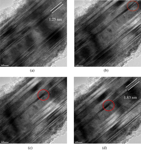
Figure shows the HRTEM image sequences which recorded the mechanical deformation process of the parallel-twinned Ni nanowires within 20 s under mechanical loading (see Supplementary Video S1). Two particular parallel-twin boundaries with twin spacing of ∼1.25 nm as indicated by the white lines in Figure (a) were chosen as the investigating object. With the increase of deformation degree, a gradual twin spacing enlarging process can be clearly observed. Figure (b,c) show a ‘zipper-opening’ like process of the two twin lamellas, and the twin spacing enlargement is marked by the red circles. This process reveals that the movement of twin planes is not in collective manner. As indicated by the white lines in Figure (d), a stable twin spacing of ∼1.83 nm (initial spacing was 1.25 nm) was finally achieved in this case. To confirm the reliability of this phenomenon, more experiments were repeated and the unzipping processes between wire-axis-parallel-twin lamellas were always observed (see another case in Supplementary Information and Video S2). We consider that the mechanism behind this twin lamella ‘unzipping’ phenomenon is the atomic layer-by-layer migration of twin boundaries caused by the gliding of partial dislocations. However, due to the technical limitation of the existing HRTEM imaging of samples during dynamic loading processes, we can hardly obtain direct evidences at atomic resolution. So in the following theoretical simulation-based investigation, we mainly focus on the mechanism of twin boundary migration. It is worth noting that the mechanical properties such as yield strength [Citation13] or fatigue [Citation61] are strongly related to the nanotwin metallic structures.
Figure 2. In situ HRTEM images of Ni nanowire under the mechanical loading: (a) Ni nanowire with wire-axis-parallel-twin boundaries. Target twin boundaries are indicated by white line, and the twin spacing between them is around 1.25 nm. (b)–(d) representative snapshots of twin space enlargement by twin boundary migration. Note that this is not collective movements of the twin planes, but a layer-by-layer climb of twin boundary. The position of twin spacing outstretching is indicated by red circles. Finally, a twin spacing of ∼1.83 nm is achieved in this case. Scale bar: 5 nm.
Molecular dynamics simulation and discussions
In this section, molecular dynamics (MD) simulations were performed to assist our understanding of the experimental observation and its associated underlying mechanisms. Figure (a,b) show our molecular dynamic simulation setup. A twinned nanowire with the same orientation as that in the experiment was constructed. The dimension of the nanowire is 12 nm in diameter and 50 nm in length. The whole system contains around 500,000 Ni atoms. The initial twin spacing was set to be 2 atom layers. Another single twin plane, which was far away (relative to the sample size) from the closely placed twin planes, was constructed as a reference. We use free boundary conditions in all three directions. The system was relaxed in an NPT ensemble (constant-temperature and constant-pressure ensemble; in which, N, number of atoms; P, pressure; T, temperature) with temperature controlled at 0 K by using Nòse-Hoover thermostat. The Pressure was set as zero in the axial direction and no pressure control was performed in other directions. To reproduce the mechanical manipulation in an experiment, two forces, which are perpendicular (5.8 × 10⁻¹¹ N) and parallel to the axial direction (4 × 10⁻¹¹ N), were applied to the right end of the nanowire (Figure (c)). To avoid the rotation or translation movements of nanowires durng loading, the left end of the nanowire was fixed by setting the mass of the atoms as infinite. We used the MEAM (modified embedded-atom method) interatomic potential created by Mishin et al. [Citation62] to describe the interaction between Ni atoms. The local crystalline structure and defects (dislocations, twin boundaries and stacking faults) were determined by using the common neighbor analysis (CNA) [Citation63] and dislocation extraction algorithm (DXA) [Citation64].
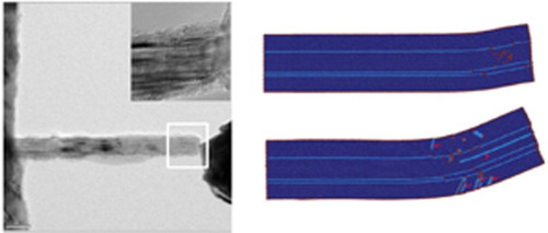
Figure 3. Representative MD snapshots of ongoing twin boundary migration under mechanical loading, along (0−1 1) plane: (a) Setup of the simulation. (b) Zoomed cross-sectional view of the (0−1 1) plane, rotated to the angle of view corresponding to our experiment. (c) simulated nanowire without stress applying. Arrows denote the direction in which forces will be applied. (d)–(g) twin spacing increasing with increasing deformation degree. Red arrows in (f) and (g) indicate other planar defects. (h) Zoomed nanowire tip of (g). The positions of partial dislocations on the twin boundary are indicated by red circles. Colors denote the local crystalline structure. Dark blue: FCC; light blue: hexagonal close-packed; red: undetectable atoms.
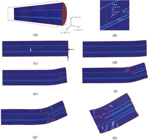
Figure (c–g) display the unzipping process of the constructed parallel-twin lamella. The simulation reproduced essentially the same observations from experiments, namely, the increasing of twin spacing with the increase of deformation (bending). The twin spacing at the top of the nanowire increased from the initial two atom layers to five layers by migration of two closely placed twin planes in opposite directions, while the single twin boundary exhibited a zig-zag form. Given that the Ni nanowires are fully packed with twin structures, those structural fluctuations cause the energetic fluctuation. Together with that the activation energy required for twin boundary migration is much lower than that for twinning, especially for nickel as a metal with high stacking fault energy (120–130 mJ m−2) [Citation45]. Therefore, upon the perturbation of external activation, twin boundary migration rather than twinning was more preferred to occur here, especially for nanostructures fully packed with parallel nanotwins already. Interestingly, planar defects, which may be stacking faults, appeared at high deformation degree (Figure (f,g)). Figure (h) represents a close view of the deformed nanowire (corresponds to the right end of Figure (g)). We consider that the twin boundary migration was caused by a slip of the partial dislocations (red atoms in red circles) on the twin planes. Thus, instead of a collective movement of twin planes, the migration of the twin boundary was achieved in a layer-by-layer manner. Lee et al. also observed a reversible twinning–detwinning phenomenon in gold nanowire under cyclic deformation dominated by a similar layer-by-layer mechanism of twin boundary movement with the help of MD simulation [Citation65]. Furthermore, dislocation and defect plane analysis shall help us to understand the mechanism of the deformation process. As an example, Figure (b–f) display the top view of one twin plane (indicated by white arrow in Figure (c) and Figure (a)). Note that we only represent the dislocations on the twin plane, other defects are intentionally hidden. There are clearly dislocations nucleated on the twin boundary. Due to the new arrangement of atoms during the dislocation nucleation, the twin plane temporarily lost its perfection (Figure (b)). Shortly after, a perfect dislocation loop was formed on the twin plane (Figure (c)). It is well known that the dislocation loop will expand when the applied shear stress is higher than a critical value which equals Gb/r (G: shear modulus, b: Burgers vector, r: radius of the dislocation loop). Note that the shear stress we applied to the nanowire is higher than this critical value. Thus, a dislocation loop expansion was well observed with further increased degree of deformation (cf. Figure (c,d)). Once the dislocation loop came through and contact the surface, the partial dislocations were annihilated, leaving two single dislocations (two half loops as indicated in Figure (d)). The left one glided from right to left along the axial direction (first step of twin plane in Figure (h), indicated by ‘1’). And the right one disappeared by further sliding due to the contact with the surface. Meanwhile, a half-loop shaped dislocation nucleated (as indicated by the white half circle in Figure (e)) and glided on the twin plane (Figure (f)), which corresponds to the second step of the twin plane in Figure (h), as indicated by ‘2’. We, therefore, believe this is a four steps process: dislocation loop nucleation, expansion, partial annihilation and further slipping. This slipping causes the climbing of the twin boundary and further increases the twin spacing. We want to note that the Burgers vectors of dislocations on the twin were 1/6<−2 1 1>, which are parallel to the axial direction. Finally, we discuss the planar defects formed at high deformation degree (indicated by red arrows in Figure (f–g)). DXA [Citation49] analysis shows that these planar defects are stacking faults (as shown in Figure (g) and Supplementary Video S3), which are consequences of deformation induced by dislocation slipping: the dislocations firstly nucleated at the surface and slipped through the nanowire, leaving stacking faults behind. We note that such surface dislocation nucleation mediated deformation mechanism has been widely reported in nanoscale materials [Citation2,Citation29,Citation67,Citation68]. Once these dislocations met with the twin boundary, further movement was inhibited, which caused the halting of the stacking fault propagation (see Supplementary Video S3). Taking the dislocation nucleation on the twin boundary into account together, we conclude that the twin boundaries act as both resources and obstacles for dislocations: dislocations nucleated on the twin boundary slip through it while the movement of other dislocations nucleated at the surface is inhibited. Therefore, it is expected that the strength and ductility of the material may be simultaneously enhanced [Citation13,Citation17,Citation22,Citation23,Citation49,Citation69] even though further experimental investigations are required.
Figure 4. Dislocation dynamics in one twin lamella plane: (a) side view of Figure (c). The twin plane to be shown is indicated by white arrows. The colors are same as that in Figure (b–f) top view of a dislocation loop nucleation, expansion and annihilation process in the indicated twin plane during mechanical loading. Only right top of the nanowire and dislocations on the twin boundary are shown. (g) DXA analysis of Figure (g). Planar defects and dislocations are shown. The defects analysis is performed by DXA [Citation49] and open-source software Paraview [Citation66] which are dedicated for visualization. Red plane: twin boundary; blue plane: stacking fault; white tube: dislocation line.
![Figure 4. Dislocation dynamics in one twin lamella plane: (a) side view of Figure 3(c). The twin plane to be shown is indicated by white arrows. The colors are same as that in Figure 3(b–f) top view of a dislocation loop nucleation, expansion and annihilation process in the indicated twin plane during mechanical loading. Only right top of the nanowire and dislocations on the twin boundary are shown. (g) DXA analysis of Figure 3(g). Planar defects and dislocations are shown. The defects analysis is performed by DXA [Citation49] and open-source software Paraview [Citation66] which are dedicated for visualization. Red plane: twin boundary; blue plane: stacking fault; white tube: dislocation line.](/cms/asset/33b15a6e-10bb-444e-9c46-e32664a13a43/tmrl_a_1383317_f0004_c.jpg)
Conclusion
In summary, we have observed the twin boundary migration in Ni nanowire upon mechanical loading and unloading, leading to the interesting ‘unzipping-zipping’ phenomenon. Such loading applied on the nanowire was mixed with both compressive and bending stress, while the bending is mainly responsible for activating multiple slip systems on the twin boundaries. A zip-form twin boundary lamella was evolving by layer-by-layer migration of twin boundary upon flexural bending. MD simulation revealed that the dislocations are mainly nucleated from two sources, twin planes and surfaces. On the twin planes, it undergoes a dislocation loop nucleation, expansion, partial annihilation and further slip process, which leads to the twin boundary migration and further increasing of the twin spacing. The dislocations nucleated at the surface (at high deformation degree) slip through the nanowire, leaving stacking fault behind. This slip is inhibited by the twin boundary. These results may provide critical new insights on understanding twin effect in the deformation mechanisms of metallic 1-D nanostructures.
Supplementary_Material
Download MS Word (529.4 KB)Disclosure statement
No potential conflict of interest was reported by the authors.
ORCID
Additional information
Funding
Related Research Data
References
- Venables J. Introduction to surface and thin film processes. Cambridge: Cambridge University Press; 2000.
- Freund LB, Suresh S. Thin film materials: stress, defect formation and surface evolution. Cambridge: Cambridge University Press; 2004.
- Wu B, Heidelberg A, Boland JJ. Mechanical properties of ultrahigh-strength gold nanowires. Nat Mater. 2005;4(7):525–529. doi: 10.1038/nmat1403
- Feng G, Nix WD, Yoon Y, et al. A study of the mechanical properties of nanowires using nanoindentation. J Appl Phys. 2006;99(7):074304. doi: 10.1063/1.2189020
- Mei QS, Lu K. Melting and superheating of crystalline solids: from bulk to nanocrystals. Prog Mater Sci. 2007;52(8):1175–1262. doi: 10.1016/j.pmatsci.2007.01.001
- Ou MN, Yang TJ, Harutyunyan SR, et al. Electrical and thermal transport in single nickel nanowire. Appl Phys Lett. 2008;92(6):063101. doi: 10.1063/1.2839572
- Tian P. Molecular dynamics simulations of nanoparticles. Annual Reports Section ‘C’ (Physical Chemistry). 2008;104(0):142–164. doi: 10.1039/b703897f
- Zhang H, Tersoff J, Xu S, et al. Approaching the ideal elastic strain limit in silicon nanowires. Sci Adv. 2016;2(8):e1501382. doi: 10.1126/sciadv.1501382
- Zhang H, Fung K-Y, Zhuang Y, et al. Fracture of silicon nanowire at ultra-large elastic strain. Acta Mechanica; Forthcoming 2017.
- Wei YJ. Anisotropic size effect in strength in coherent nanowires with tilted twins. Phys Rev B. 2011;84(1):014107. doi: 10.1103/PhysRevB.84.014107
- Li SZ, Ding XD, Deng JK, et al. Superelasticity in bcc nanowires by a reversible twinning mechanism. Phys Rev B. 2010;82(20):205435. doi: 10.1103/PhysRevB.82.205435
- Yu Q, Shan ZW, Li J, et al. Strong crystal size effect on deformation twinning. Nature. 2010;463(7279):335–338. doi: 10.1038/nature08692
- Wang J, Sansoz F, Huang J, et al. Near-ideal theoretical strength in gold nanowires containing angstrom scale twins. Nat Commun. 2013;4:1742. doi: 10.1038/ncomms2768
- Lu Y, Song J, Huang JY, et al. Fracture of Sub-20nm ultrathin gold nanowires. Adv Funct Mater. 2011;21(20):3982–3989. doi: 10.1002/adfm.201101224
- Jang D, Li X, Gao H, et al. Deformation mechanisms in nanotwinned metal nanopillars. Nat Nanotechnol. 2012;7(9):594–601. doi: 10.1038/nnano.2012.116
- Chen M, Ma E, Hemker KJ, et al. Deformation twinning in nanocrystalline aluminum. Science. 2003;300(5623):1275–1277. doi: 10.1126/science.1083727
- Lu L, Shen Y, Chen X, et al. Ultrahigh strength and high electrical conductivity in copper. Science. 2004;304(5669):422–426. doi: 10.1126/science.1092905
- Shen YF, Lu L, Lu QH, et al. Tensile properties of copper with nano-scale twins. Scr Mater. 2005;52(10):989–994. doi: 10.1016/j.scriptamat.2005.01.033
- Zhu YT, Liao XZ, Srinivasan SG, et al. Nucleation of deformation twins in nanocrystalline face-centered-cubic metals processed by severe plastic deformation. J Appl Phys. 2005;98(3):034319. doi: 10.1063/1.2006974
- Wu X, Zhu YT, Chen MW, et al. Twinning and stacking fault formation during tensile deformation of nanocrystalline Ni. Scr Mater. 2006;54(9):1685–1690. doi: 10.1016/j.scriptamat.2005.12.045
- Zhu YT, Liao XZ, Wu XL. Deformation twinning in bulk nanocrystalline metals: experimental observations. JOM. 2008;60(9):60–64. doi: 10.1007/s11837-008-0120-1
- Lu L, Chen X, Huang X, et al. Revealing the maximum strength in nanotwinned copper. Science. 2009;323(5914):607–610. doi: 10.1126/science.1167641
- Lu K, Lu L, Suresh S. Strengthening materials by engineering coherent internal boundaries at the nanoscale. Science. 2009;324(5925):349–352. doi: 10.1126/science.1159610
- Zhu YT, Wu XL, Liao XZ, et al. Twinning partial multiplication at grain boundary in nanocrystalline FCC metals. Appl Phys Lett. 2009;95(3):031909. doi: 10.1063/1.3187539
- Li X, Wei Y, Lu L, et al. Dislocation nucleation governed softening and maximum strength in nano-twinned metals. Nature. 2010;464(7290):877–880. doi: 10.1038/nature08929
- Zhu YT, Liao XZ, Wu XL. Deformation twinning in nanocrystalline materials. Prog Mater Sci. 2012;57(1):1–62. doi: 10.1016/j.pmatsci.2011.05.001
- Wang YM, Sansoz F, LaGrange T, et al. Defective twin boundaries in nanotwinned metals. Nat Mater. 2013;12(8):697–702. doi: 10.1038/nmat3646
- Wu F, Zhu YT, Narayan J. Macroscopic twinning strain in nanocrystalline Cu. Mater Res Lett. 2014;2(2):63–69. doi: 10.1080/21663831.2013.862874
- Wang LH, Lu Y, Kong DL, et al. Dynamic and atomic-scale understanding of the twin thickness effect on dislocation nucleation and propagation activities by in situ bending of Ni nanowires. Acta Mater. 2015;90:194–203. doi: 10.1016/j.actamat.2015.02.002
- Li XY, Dao M, Eberl C, et al. Fracture, fatigue, and creep of nanotwinned metals. MRS Bull. 2016;41(4):298–304. doi: 10.1557/mrs.2016.65
- Li N, Wang JW, Mao S, et al. In situ nanomechanical testing of twinned metals in a transmission electron microscope. MRS Bull. 2016;41(4):305–313. doi: 10.1557/mrs.2016.66
- Furnish TA, Hodge AM. On the mechanical performance and deformation of nanotwinned Ag. APL Mater. 2014;2(4):046112. doi: 10.1063/1.4873215
- Qin Q, Yin S, Cheng G, et al. Recoverable plasticity in penta-twinned metallic nanowires governed by dislocation nucleation and retraction. Nat Commun. 2015;6:5983. doi: 10.1038/ncomms6983
- Chang TH, Cheng GM, Li CJ, et al. On the size-dependent elasticity of penta-twinned silver nanowires. Extreme Mech Lett. 2016;8:177–183. doi: 10.1016/j.eml.2016.03.007
- Cui Y, Zhong ZH, Wang DL, et al. High performance silicon nanowire field effect transistors. Nano Lett. 2003;3(2):149–152. doi: 10.1021/nl025875l
- Snider GS, Williams RS. Nano/CMOS architectures using a field-programmable nanowire interconnect. Nanotechnology. 2007;18(3):035204. doi: 10.1088/0957-4484/18/3/035204
- Lee J, Lee P, Lee H, et al. Very long Ag nanowire synthesis and its application in a highly transparent, conductive and flexible metal electrode touch panel. Nanoscale. 2012;4(20):6408–6414. doi: 10.1039/c2nr31254a
- Wang JG, Tian ML, Mallouk TE, et al. Microtwinning in template-synthesized single-crystal metal nanowires. J Phys Chem B. 2004;108(3):841–845. doi: 10.1021/jp035068q
- Bernardi M, Raja SN, Lim SK. Nanotwinned gold nanowires obtained by chemical synthesis. Nanotechnology. 2010;21(28):285607. doi: 10.1088/0957-4484/21/28/285607
- Lu Y, Peng C, Ganesan Y, et al. Quantitative in situ TEM tensile testing of an individual nickel nanowire. Nanotechnology. 2011;22(35):355702. doi: 10.1088/0957-4484/22/35/355702
- Zhang L, Petit T, Lu Y, et al. Controlled propulsion and cargo transport of rotating nickel nanowires near a patterned solid surface. ACS Nano. 2010;4(10):6228–6234. doi: 10.1021/nn101861n
- Zhang H, Jiang C, Lu Y. Low-Cycle fatigue testing of Ni nanowires based on a micro-mechanical device. Exp Mech. 2017;57(3):495–500. doi: 10.1007/s11340-016-0199-1
- Peng C, Ganesan Y, Lu Y, et al. Size dependent mechanical properties of single crystalline nickel nanowires. J Appl Phys. 2012;111(6):063524. doi: 10.1063/1.3698625
- Peng C, Zhong Y, Lu Y, et al. Strain rate dependent mechanical properties in single crystal nickel nanowires. Appl Phys Lett. 2013;102(8):083102. doi: 10.1063/1.4793481
- Carter C, Holmes S. The stacking-fault energy of nickel. Philos Mag. 1977;35(5):1161–1172. doi: 10.1080/14786437708232942
- Deng C, Sansoz F. Fundamental differences in the plasticity of periodically twinned nanowires in Au, Ag, Al, Cu, Pb and Ni. Acta Mater. 2009;57(20):6090–6101. doi: 10.1016/j.actamat.2009.08.035
- Deng C, Sansoz F. A new form of pseudo-elasticity in small-scale nanotwinned gold. Extreme Mech Lett. 2016;8:201–207. doi: 10.1016/j.eml.2015.12.004
- Cao AJ, Wei YG, Mao SX. Deformation mechanisms of face-centered-cubic metal nanowires with twin boundaries. Appl Phys Lett. 2007;90(15):151909. doi: 10.1063/1.2721367
- Deng C, Sansoz F. Enabling ultrahigh plastic flow and work hardening in twinned gold nanowires. Nano Lett. 2009;9(4):1517–1522. doi: 10.1021/nl803553b
- Frøseth AG, Derlet PM, Van Swygenhoven H. Twinning in nanocrystalline FCC metals. Adv Eng Mater. 2005;7(1-2):16–20. doi: 10.1002/adem.200400163
- Shetty M. Dislocations and mechanical behaviour of materials. Delhi: PHI Learning Pvt. Ltd.; 2013.
- Shan ZW, Wiezorek JMK, Stach EA, et al. Dislocation dynamics in nanocrystalline nickel. Phys. Rev Lett. 2007;98(9):095502. doi: 10.1103/PhysRevLett.98.095502
- Yu Q, Qi L, Chen K, et al. The nanostructured origin of deformation twinning. Nano Lett. 2012;12(2):887–892. doi: 10.1021/nl203937t
- Sun J, He L, Lo YC, et al. Liquid-like pseudoelasticity of sub-10-nm crystalline silver particles. Nat Mater. 2014;13(11):1007–1012. doi: 10.1038/nmat4105
- Liu B-Y, Wang J, Li B, et al. Twinning-like lattice reorientation without a crystallographic twinning plane. Nat Commun. 2014;5:3297.
- Yu Q, Legros M, Minor AM. In situ TEM nanomechanics. MRS Bull. 2015;40(01):62–70. doi: 10.1557/mrs.2014.306
- Wang J, Zeng Z, Weinberger CR, et al. In situ atomic-scale observation of twinning-dominated deformation in nanoscale body-centred cubic tungsten. Nat Mater. 2015;14(6):594–600. doi: 10.1038/nmat4228
- Ramachandramoorthy R, Bernal R, Espinosa HD. Pushing the envelope of In situ transmission electron micro-scopy. ACS Nano. 2015;9(5):4675–4685. doi: 10.1021/acsnano.5b01391
- Zhang Z, Sheng H, Wang Z, et al. Dislocation mechanisms and 3D twin architectures generate exceptional strength-ductility-toughness combination in CrCoNi medium-entropy alloy. Nat Commun. 2017;8:14390. doi: 10.1038/ncomms14390
- Zheng K, Wang C, Cheng YQ, et al. Electron-beam-assisted superplastic shaping of nanoscale amorphous silica. Nat Commun. 2010;1:24.
- Liu L, Wang J, Gong SK, et al. Atomistic observation of a crack tip approaching coherent twin boundaries. Sci Rep. 2015;4:4397. doi: 10.1038/srep04397
- Mishin Y, Farkas D, Mehl MJ, et al. Interatomic potentials for monoatomic metals from experimental data and ab initio calculations. Phys Rev B. 1999;59(5):3393–3407. doi: 10.1103/PhysRevB.59.3393
- Faken D, Jónsson H. Systematic analysis of local atomic structure combined with 3D computer graphics. Comput Mater Sci. 1994;2(2):279–286. doi: 10.1016/0927-0256(94)90109-0
- Stukowski A, Albe K. Extracting dislocations and non-dislocation crystal defects from atomistic simulation data. Modell Simul Mater Sci Eng. 2010;18(8):085001. doi: 10.1088/0965-0393/18/8/085001
- Lee S, Im J, Yoo Y, et al. Reversible cyclic deformation mechanism of gold nanowires by twinning-detwinning transition evidenced from in situ TEM. Nat Commun. 2014;5:3033.
- Ayachit U. The paraview guide: a parallel visualization application. New York: Kitware; 2015.
- Lu Y, Song J, Huang J, et al. Surface dislocation nucleation mediated deformation and ultrahigh strength in sub-10-nm gold nanowires. Nano Res. 2011;4(12):1261–1267. doi: 10.1007/s12274-011-0177-y
- Roos B, Kapelle B, Richter G, et al. Surface dislocation nucleation controlled deformation of Au nanowires. Appl Phys Lett. 2014;105(20):201908. doi: 10.1063/1.4902313
- Wei Y, Li Y, Zhu L, et al. Evading the strength-ductility trade-off dilemma in steel through gradient hierarchical nanotwins. Nat Commun. 2014;5:3580.