
Abstract
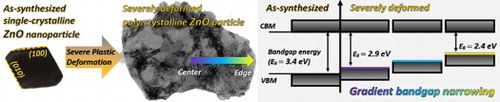
Gradient nanostructured metallic materials with a gradual change of grain boundary and dislocation density display unprecedent mechanical properties. Herein, we uncover a gradient of point defects concentration and concomitant gradient bandgap (Eg) narrowing in metal oxide nanoparticles processed by a combination of severe shearing and frictional sliding deformation. Using the valence electron-energy loss spectroscopy technique, we find a gradual decrease of Eg from 2.93 eV in the interior to 2.43 eV at the edge of the high-pressure torsion processed ZnO flake-shaped particle. This work paves the way to strain engineering of gradient-structured metal oxide semiconductors for unique functional properties.
IMPACT STATEMENT
We uncover a gradient of oxygen vacancy concentration and concomitant bandgap narrowing in an individual metal oxide nanoparticle processed by a combination of severe shearing and frictional sliding deformation.
GRAPHICAL ABSTRACT
1. Introduction
Gradient-structured materials represent an emerging class of architectured materials [Citation1] that have garnered increased attention due to their notable structural performance such as evaded strength-ductility trade-off dilemma and enhanced fatigue properties [Citation2–5]. This is attributed to the gradient of grain size, typically from nanostructured or ultrafine-grained surface layer to coarse-grained bulk interior. The two main techniques that have been utilized to produce extreme surface grain refinement and gradient structures are severe plastic deformation (SPD) and dynamic plastic deformation (DPD) [Citation2–6]. However, in addition to high density of dislocations and stacking faults/twin boundaries that contribute to surface grain fragmentation and subdivision, processing of materials with these techniques also results in excess concentration of point defects [Citation6,Citation7]. Theoretically, the gradient of their concentration could also be utilized for design of unique properties.
The formation of vacancies during plastic deformation is a result of dislocation interactions, and it is expected to be similar both in metals and ceramics, provided the vacancy formation energies are similar. However, the kinetics of vacancy diffusion depends on vacancy migration energy. In most common metals, the vacancy formation and migration energies are nearly equal. For example, in coinage metals (Au, Ag, and Cu) both vacancy formation and migration energies are in the range of 0.8 to 1.0 eV. This is why in these metals the vacancies are mobile at room temperature, and the gradients of their concentration cannot be retained for a long time. In ceramics, the situation may be different. For example, in wurtzite ZnO the formation energy of the neutral oxygen vacancy is about 0.73 to 1.0 eV, while its migration energy is about 2.4 eV [Citation8]. Thus, during plastic deformation of ZnO the vacancies should be produced with the same easy as in coinage metals, yet their migration will be ‘frozen’ at room temperature. This enables engineering stable vacancy gradients in ceramic materials by the SPD techniques.
Though oxides are brittle under normal conditions and possess much less formability than their metallic counterparts, substantial ductility can be gained under high hydrostatic confining pressure, which facilitates the transformation from micro-cracking to plastic slip and inelastic relaxation, and reduces the critical resolved shear stress for activation of slip systems [Citation9–11]. For example, extensive plasticity of α-alumina under hydrostatic pressure of about 3 GPa was reported by Percy Bridgman already in the year 1947 [Citation12]. The SPD techniques such as high-pressure torsion (HPT) have been widely employed to manipulate the microstructure of oxides (see Ref. [Citation11] for review). In addition to grain refinement and phase transformations, formation of oxygen vacancies during HPT processing has been observed in a range of oxides nanoparticles including BaTiO3 [Citation13], TiO2 [Citation14], ZnO [Citation15], Al2O3 [Citation16], Y2O3 [Citation17], and GaN–ZnO [Citation18].
Oxygen vacancies can affect the functional properties of metal oxides such as the bandgap width, because the elastic strain of the lattice produced by these point defects is coupled to the electronic band structure [Citation19]. Therefore, producing a gradient of point defects concentration in metal oxide can result in the gradient of the material functional properties. In the present work, we demonstrate a gradient bandgap narrowing phenomenon in SPD-processed individual ZnO particles exhibiting a continuous increase of oxygen vacancy concentration from the interior to the edge of the particle.
2. Materials and methods
ZnO particles were sandwiched between two Cu disks and were processed by HPT at a compressive pressure of 5 GPa for 5 turns [Citation10]. To measure the evolution of bandgap energy and oxygen vacancy concentration in the HPT-processed ZnO particles, we used the electron energy-loss spectroscopy (EELS) technique in a monochromated scanning transmission electron microscope (STEM) (for a detailed description of the experimental methods, see Supporting Information and Figure S1 therein).
3. Results and discussion
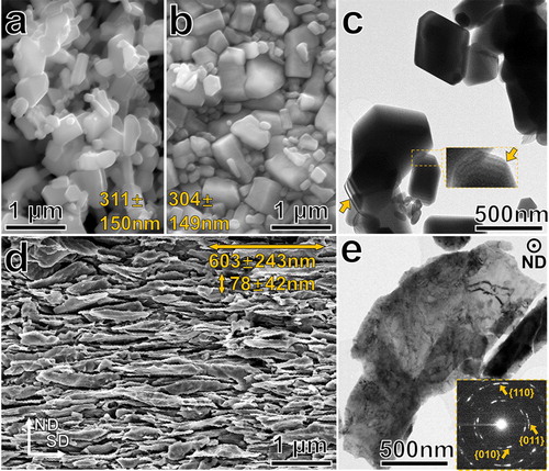
The as-synthesized single-crystalline ZnO particles obtained via indirect or French process exhibit a typical nodular shape [Citation20] and an average size of 311 ± 150 nm (see Figure (a) and Figure S2 for TEM characterization of the nearly Wulff-shaped ZnO single-crystals). Since the hardness of single-crystalline ZnO is close to 5 GPa, compressing the agglomerates of ZnO nanoparticles under the pressure of 5 GPa only introduced consolidation, but did not deform or break the particles and did not change their average size (Figure (b)). However, by conducting HPT process, significant plastic deformation was introduced into the ZnO particles and their morphology transformed from equiaxed- to flake-like one. As shown in Figure (c), the as-synthesized equiaxed ZnO particles are not transparent under bright-field (BF) TEM imaging conditions, and thickness fringes can be observed at the edge of the particles. On the other hand, an HPT-processed ZnO particle shown in Figure (e) is transparent and polycrystalline, indicating that ZnO particles have undergone severe plastic deformation and that the deformation was accompanied by grain fragmentation. The selected area diffraction pattern (SADP) taken from the deformed particle indicates that it is polycrystalline and no phase transformation from hexagonal wurtzite to rocksalt phase occurred. Finally, it is interesting to note that we performed SADP on several deformed particles and no diffraction spots or rings from {002} lattice planes were observed due to the strong basal texture developed during the HPT processing.
Figure 1. The change of ZnO particles morphology and microstructure caused by HPT processing. SEM images of as-synthesized (a) and compacted (b) ZnO particles with average particle sizes of 311 ± 150 nm and 304 ± 149 nm, respectively; (c) a BF-TEM image of as-synthesized ZnO particles; insert and arrows highlight the thickness fringes at the edge of the particles; (d) a SEM image of HPT-processed ZnO particles having average dimensions of 603 ± 243 nm and 78 ± 42 nm along the shearing direction (SD) and normal direction (ND), respectively; (e) a BF-TEM image of an HPT-processed ZnO particle; insert shows a SADP taken from the particle.
During the HPT processing, in addition to severe shear deformation of individual ZnO particles, relative frictional sliding between them and subsequent consolidation of the particle agglomerates also occurred [Citation21]. In the latter process, the edge of the flake-shaped particles could develop a wedge-like shape with decreasing thickness, enabling better particles packing and increase of the compact density, as schematically illustrated in Figure (a). It has been revealed that friction deformation by relative sliding under SPD condition (hydrostatic pressure and shear strain) contributes to higher extent of lattice strain and plastic instability of the sliding surfaces, as compared to a more homogeneous deformation in the interior of the processed material [Citation22]. In the present case, we anticipate higher density of defects at the surfaces and edge regions of the HPT-processed ZnO particles.
Figure 2. The wedge-like shape of the edge region on HPT-processed ZnO particles. (a) a schematic illustration of the frictional sliding, shear deformation and consolidation of the HPT-processed ZnO particles; (b) an ADF-STEM image of two HPT-processed ZnO particles with an overlap region, indicating that frictional sliding may occur between them; (c) a map of the relative thickness, t/λ, taken from a particle edge region highlighted in (b). The absolute thickness changes gradually from 0.32λ (29 nm) to 1.14λ (104 nm) from the edge to the interior of the particle, within a distance of 225 nm along the particle surface.
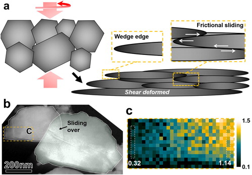
The wedge-like shape of the edge region was confirmed by the relative thickness map, Figure (b,c). The mean free path of inelastically scattered electrons, λ, was estimated to be 91 or 149 nm, using two formulas derived with the aid of the log-ratio method [Citation23,Citation24]. Based on the analysis of SEM micrographs, the maximum thickness of the deformed ZnO particles is about 120 nm. Therefore, we selected λ = 91 nm, as the other estimate (λ = 149 nm) leads to an estimated thickness of 170 nm in the center region of the ZnO particle, much higher than the measured value of 120 nm.
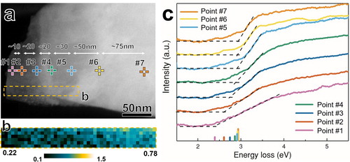
For the measurement of bandgap at specific sites on an HPT-processed ZnO particle, valence EEL spectra (VEELS) were collected. To extract the bandgap value, the power-law model was used to subtract the background signal using a fitting range 1.5 to 2.4 eV. It is worth noting that the effect of subtraction range on the determined value of bandgap onset of ZnO is small, and the error is within 0.04 eV [Citation25]. Then, we applied the linear fit method to determine the bandgap energy, since this method overcomes the effects of specimen thickness variation and reduces the Cerenkov effect [Citation26–28]. In this method, the bandgap energy is estimated by finding the intersection point of a straight horizontal line corresponding to the averaged background level (after subtraction) with a linear fit to the onset of the loss signal spectrum. Finally, according to analysis of Erni and Browning [Citation29], since normalized emission rate for ZnO is 0.69 (having the maximum real part of dielectric constant of 3.5 to 5 [Citation30–32]) and below the critical value of 0.9, Cerenkov radiation generation is strongly damped.
As shown in Figure , the edge region of the HPT-processed ZnO particle displays a gradient bandgap narrowing phenomenon. The bandgap values change from 2.43 ± 0.06, to 2.61 ± 0.05, 2.74 ± 0.04, 2.86 ± 0.04, 2.91 ± 0.03, 2.92 ± 0.03 and 2.93 ± 0.03 eV, from point #1 to #7, respectively. Significant bandgap change is found between the points #1 and #5, which are within about 120 nm from the particle edge, corresponding to the relative thickness change from 0.22λ (20 nm) to 0.78λ (71 nm). Moving from point #5 to #7 towards the interior of the particle results in the bandgap value reaching a plateau at 2.9 eV. This bandgap variation from 2.4 to 2.9 eV is in good agreement with the appreciable tail absorbance below the bandgap onset energy of 2.8 eV measured by ultraviolet-visible diffuse reflectance spectroscopy in wurtzite ZnO compacts HPT-processed under compressive pressure of 3 GPa [Citation15]. It is worth noting that the bandgap onset would gradually redshift to lower energies with increasing thickness due to stronger retardation from Cerenkov radiation in thicker regions [Citation26,Citation33]. In the present case, the bandgap onsets exhibit a blueshift with increasing thickness, indicating little effect of Cerenkov radiation.
Figure 3. Gradient bandgap narrowing at the edge of an HPT-processed ZnO particle. (a) the ADF image of a deformed ZnO particle on which seven EELS acquisition locations are labeled; (b) a relative thickness map showing the t/λ changes from 0.22 at the outermost edge to 0.78 within 120 nm towards the interior of the particle; (c) seven VEEL spectra after ZLP and background subtraction. Note the increase of slopes of the low-loss spectra from point #1 to #7 with increasing thickness. Furthermore, the intensity of the humps before the bandgap onsets increased along with increasing thickness due to greater Cerenkov and surface effects.
Further possible reasons for the observed bandgap narrowing include: (i) Cu diffusion into ZnO during HPT processing and its chemical modification [Citation34], and (ii) gradient of dislocations density across the ZnO particle and concomitant variation of the bandgap [Citation35]. As for the former reason, our previous study reveals that no intermixing occurred between the cladding Cu disk and ZnO clusters [Citation10]. As for the latter reason, it was shown in Ref. [Citation35] that the effect of dislocations on the bandgap of ZnO is only minor, i.e. an increase in dislocations density form ∼2.4 × 10¹⁵ to ∼5.3 × 10¹⁵ 1/m2 causes a minor bandgap narrowing from 3.26 to 3.20 eV, one order of magnitude smaller than observed in the present work. Therefore, the gradient bandgap narrowing observed in the present work can neither be attributed to the chemical doping nor to the dislocations density variations.
Another possible explanation for the gradient bandgap narrowing is a gradual increase of oxygen vacancy (VO) concentration from the center towards the edge of the particle. Indeed, it has been widely reported that VO contribute to bandgap narrowing [Citation14–17]. The first-principles calculations of Razavi-Khosroshah et al. demonstrated that introducing 6.25% of VO into wurtzite ZnO could reduce its bandgap onset energy from 3.22 to 2.91 eV [Citation15]. By tuning the oxygen deficiency in ZnO coatings, Zhang et al. revealed a reduction of bandgap energy to ∼2.5 eV in ZnO0.952 with the VO concentration of 4.8% [Citation36,Citation37]. Finally, it has been widely reported that HPT process is capable of inducing high vacancy concentration that is comparable to the equilibrium vacancy concentration in respective material at its melting point (Tm) [Citation38]. This is a maximum vacancy concentration that a solid can sustain without melting or amorphization [Citation39]. Our estimates of the equilibrium VO concentration in ZnO at Tm = 2248 K yielded the range of 4.3% to 7.9% (see Supporting Information). Therefore, a reduction of bandgap energy to ∼2.43 eV can be caused by oxygen vacancies produced during HPT processing.
In this work, due to higher strain and larger fraction of friction-affected surface area, the thinner edge region is expected to possess higher defects density than that of the central, thicker region of the flake-shaped particle. The variation of VO concentration can be revealed by the electron energy-loss near-edge structure (ELNES) of O K-edge which represents the p-projected density of unoccupied states of the O atoms. Any change in the local symmetry will affect the Zn 3d-O 2p covalent-bonding interaction and the orbital hybridization [Citation40,Citation41]. A reduction of the p–d interaction by disorder would lead to an upward shift of the valence band maximum (VBM), which can be revealed by the change of the features in ELNES [Citation42]. As seen in Figure (a), the peak a of O K-edge splits into four characteristic peaks due to the ligand-field and exchange interactions, and corresponds to the transitions towards d-p hybridized vacant states, i.e. 2t2 and 3e states [Citation43]. The two main characteristic peaks a1 at 534.8 eV and a2 at 536.9 eV, with an energy separation of 2.1 eV, are the signature of the tetrahedral arrangement of the O atoms [Citation44]. The relative intensity of these two peaks is strongly influenced by the VO concentration and the ratio of a1/a2 increases with increasing VO concentration [Citation45–47]. By measuring the intensity of a1 (in the range of 533.5 to 535.5 eV) and a2 (in the range of 536.0 to 538.0 eV), it is found that the ratio of a1/a2 increases from 84.7% in the interior region of the particle (0.64λ) to 85.7% at 0.39λ, and 86.3% at 0.22λ. Therefore, the gradient increase of VO concentration contributes to the upward shift of the VBM and gradient bandgap narrowing.
Figure 4. The evolution of valence band maximum and conduction band minimum at the edge region studied by core-loss EELS of (a) O K-edge and (b) Zn L2,3-edge. The spectra are averaged from the strips shown in the insert in (b), and the background signals were subtracted. Note the arrow in (a) pointing at the characteristic peak a1.
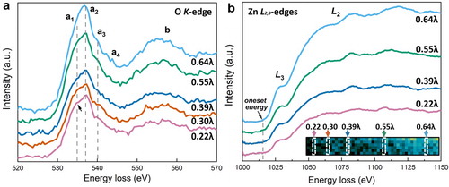
In addition, we also checked the possible contribution of downward shift of conduction band minimum (CBM) to the bandgap narrowing. As seen in Figure (b), the onset energy of Zn L3-edge at four positions remained nearly constant at 1015 eV. This indicates that the CBM did not shift. This is expected because the shift of CBM is mainly governed by the change of coordination symmetry of the Zn atoms [Citation28,Citation48]; since no phase transformation or significant structural disorder was detected in the SADPs of the HPT-processed ZnO particles, the Zn coordination symmetry was not affected.
4. Conclusion and outlook
In conclusion, a gradient bandgap energy narrowing phenomenon in individual HPT-processed flake-shaped ZnO nanoparticles was revealed employing the STEM-EELS technique. The bandgap onset energy decreased from 2.93 eV in the interior to 2.43 eV at the edge of the particle within about 200 nm. The underpinning mechanism is the gradient of oxygen vacancy concentration which was induced by the combination of severe shearing and frictional sliding deformation. The edge of the particle underwent higher plastic deformation than that of the interior region, as the thicknesses of the edge and central regions of the studied particle are about 20 and 104 nm, respectively.
The gradient point defects distribution not only expands the family of gradient-structured materials, but also provides a new designing route for bandgap engineering of semiconductor materials. For example, regarding the photovoltaics applications, single-bandgap materials such as Si (Eg = 1.12 eV) and CuO (Eg = 1.4 eV) exhibit maximum theoretical solar to electrical power conversion efficiency at about 33% and 31%, respectively [Citation49]. Solar light with photon energies greater than the bandgap is partially absorbed and partially lost as heat. Therefore, to efficiently absorb broader energy spectrum, multilayer solar cells built of the layers with different bandgaps have been designed, known as multi-junction cells [Citation50]. Gradient-bandgap materials can provide an alternative, lower-cost way of capturing higher fraction of the sunlight. The SPD-based method developed in this work to generate the gradients of the point defect distribution and the bandgap can be applied to a large number of semiconductor materials. Large bandgap gradients can be achieved by tailoring the processing parameters (e.g. compressive pressure, shearing and frictional strain). We hope that our work will stimulate the use of materials with engineered bandgap gradients in photovoltaic applications.
Supplemental Material
Download PDF (441.9 KB)Acknowledgements
The work was supported by the Ministry of Science & Technology, Israel (grant 3-16534), and by Russian Foundation for Basic Research (grant 19-58-06002). YQ would like to thank the support by Technion-Guangdong Postdoctoral Fellowship.
Disclosure statement
No potential conflict of interest was reported by the author(s).
Additional information
Funding
References
- Estrin Y, Bréchet Y, Dunlop J, et al. Architectured materials in nature and engineering. Cham, Switzerland: Springer Nature Switzerland AG; 2019.
- Lu K. Making strong nanomaterials ductile with gradients. Science. 2014;345(6203):1455–1456.
- Yang M, Pan Y, Yuan F, et al. Back stress strengthening and strain hardening in gradient structure. Mater Res Lett. 2016;4(3):145–151.
- Wu X, Jiang P, Chen L, et al. Extraordinary strain hardening by gradient structure. Proc Natl Acad Sci USA. 2014;111(20):7197–7201.
- Lu K. Stabilizing nanostructures in metals using grain and twin boundary architectures. Nat Rev Mater. 2016;1(5):1–13.
- Estrin Y, Vinogradov A. Extreme grain refinement by severe plastic deformation: a wealth of challenging science. Acta Mater. 2013;61(3):782–817.
- Setman D, Schafler E, Korznikova E, et al. The presence and nature of vacancy type defects in nanometals detained by severe plastic deformation. Mater Sci Eng A. 2008;493(1):116–122.
- Deng B, Rosa AL, Frauenheim T, et al. Oxygen vacancy diffusion in bare ZnO nanowires. Nanoscale. 2014;6(20):11882–11886.
- Amodeo J, Carrez P, Cordier P. Modelling the effect of pressure on the critical shear stress of MgO single crystals. Phil Mag. 2012;92(12):1523–1541.
- Qi Y, Kosinova A, Kilmametov AR, et al. Plastic flow and microstructural instabilities during high-pressure torsion of Cu/ZnO composites. Mater Charact. 2018;145:389–401.
- Edalati K. Review on recent advancements in severe plastic deformation of oxides by high-pressure torsion (HPT). Adv Eng Mater. 2019;21(1):1800272.
- Bridgman P. The effect of hydrostatic pressure on the fracture of brittle substances. J Appl Phys. 1947;18(2):246–258.
- Edalati K, Arimura M, Ikoma Y, et al. Plastic deformation of BaTiO3 ceramics by high-pressure torsion and changes in phase transformations, optical and dielectric properties. Mater Res Lett. 2015;3(4):216–221.
- Razavi-Khosroshahi H, Edalati K, Hirayama M, et al. Visible-light-driven photocatalytic hydrogen generation on nanosized TiO2-II stabilized by high-pressure torsion. ACS Catal. 2016;6(8):5103–5107.
- Razavi-Khosroshahi H, Edalati K, Wu J, et al. High-pressure zinc oxide phase as visible-light-active photocatalyst with narrow band gap. J Phys Chem A. 2017;5(38):20298–20303.
- Edalati K, Fujita I, Takechi S, et al. Photocatalytic activity of aluminum oxide by oxygen vacancy generation using high-pressure torsion straining. Scr Mater. 2019;173:120–124.
- Razavi-Khosroshahi H, Edalati K, Emami H, et al. Optical properties of nanocrystalline monoclinic Y2O3 stabilized by grain size and plastic strain effects via high-pressure torsion. Inorg Chem. 2017;56(5):2576–2580.
- Edalati K, Uehiro R, Takechi S, et al. Enhanced photocatalytic hydrogen production on GaN–ZnO oxynitride by introduction of strain-induced nitrogen vacancy complexes. Acta Mater. 2020;185:149–156.
- Cai W, Nix WD. Imperfections in crystalline solids. Cambridge: Cambridge University Press; 2016.
- Moezzi A, McDonagh AM, Cortie MB. Zinc oxide particles: synthesis, properties and applications. Chem Eng J. 2012;185:1–22.
- Xia K. Consolidation of particles by severe plastic deformation: mechanism and applications in processing bulk ultrafine and nanostructured alloys and composites. Adv Eng Mater. 2010;12(8):724–729.
- Qi Y, Kosinova A, Kilmametov AR, et al. Stabilization of ultrafine-grained microstructure in high-purity copper by gas-filled pores produced by severe plastic deformation. Scr Mater. 2020;178:29–33.
- Iakoubovskii K, Mitsuishi K, Nakayama Y, et al. Thickness measurements with electron energy loss spectroscopy. Micr Res Tech. 2008;71(8):626–631.
- Malis T, Cheng S, Egerton R. EELS log-ratio technique for specimen-thickness measurement in the TEM. J Electron Microsc Tech. 1988;8(2):193–200.
- Zhan W. Band gap mapping of alloyed ZnO using probe-corrected and monochromated STEM-EELS [dissertation]. University of Oslo; 2018.
- Park J, Heo S, Chung J-G, et al. Bandgap measurement of thin dielectric films using monochromated STEM-EELS. Ultramicroscopy. 2009;109(9):1183–1188.
- Virdi KS, Kauffmann Y, Ziegler C, et al. Band gap extraction from individual two-dimensional perovskite nanosheets using valence electron energy loss spectroscopy. J Phys Chem C. 2016;120(20):11170–11179.
- Wei J, Ogawa T, Feng B, et al. Direct measurement of electronic band structures at oxide grain boundaries. Nano Lett. 2020;20(4):2530–2536.
- Erni R, Browning ND. The impact of surface and retardation losses on valence electron energy-loss spectroscopy. Ultramicroscopy. 2008;108(2):84–99.
- Meyer B. ZnO: dielectric constants. New data and updates for IV–IV, III–V, II–VI and I–VII compounds, their mixed crystals and diluted magnetic semiconductors. Berlin Heidelberg: Springer; 2011. p. 593–593.
- Sarkar A, Ghosh S, Chaudhuri S, et al. Studies on electron transport properties and the Burstein-Moss shift in indium-doped ZnO films. Thin Solid Films. 1991;204(2):255–264.
- Sun J, Wang H-T, He J, et al. Ab initio investigations of optical properties of the high-pressure phases of ZnO. Phys Rev B. 2005;71(12):125132.
- Huang MR, Erni R, Lin H-Y, et al. Characterization of wurtzite ZnO using valence electron energy loss spectroscopy. Phys Rev B. 2011;84(15):155203.
- Chakraborty M, Ghosh A, Thangavel R. Experimental and theoretical investigations of structural and optical properties of copper doped ZnO nanorods. J Sol-Gel Technol. 2015;74(3):756–764.
- Chattopadhyay S, et al. Dislocations and particle size governed bandgap and ferromagnetic ordering in Ni-doped ZnO nanoparticles synthesized via co-precipitation. Ceram Int. 2019;45(17):23341–23354.
- Zhang C, Geng X, Liao H, et al. Room-temperature nitrogen-dioxide sensors based on ZnO1−x coatings deposited by solution precursor plasma spray. Sens Actuators B Chem. 2017;242:102–111.
- Wang J, Chen R, Xiang L, et al. Synthesis, properties and applications of ZnO nanomaterials with oxygen vacancies: a review. Ceram Int. 2018;44(7):7357–7377.
- Zehetbauer M, Steiner G, Schafler E, et al. Deformation induced vacancies with severe plastic deformation: measurements and modelling. Mater Sci Forum. 2006;503–504:57–64.
- Fecht H. Defect-induced melting and solid-state amorphization. Nature. 1992;356(6365):133–135.
- Ahn CC. Transmission electron energy loss spectrometry in materials science and the EELS atlas. Weinheim: Wiley-VCH; 2004.
- Lee JH, Lee WJ, Lee SH, et al. Atomic-scale origin of piezoelectricity in wurtzite ZnO. Phys Chem Chem Phys. 2015;17(12):7857–7863.
- Ellmer K, Klein A, Rech B. Transparent conductive zinc oxide: basics and applications in thin film solar cells. Vol. 104. Berlin Heidelberg: Springer Science & Business Media; 2007.
- Ding Y, Wang ZL. Electron energy-loss spectroscopy study of ZnO nanobelts. J Electron Microsc Tech. 2005;54(3):287–291.
- Jollet F, Noguera C, Thromat N, et al. Electronic structure of yttrium oxide. Phys Rev B. 1990;42(12):7587.
- Travlos A, Boukos N, Apostolopoulos G, et al. Oxygen vacancy ordering in epitaxial layers of yttrium oxide on Si (001). Appl Phys Lett. 2003;82(23):4053–4055.
- Ou DR, Mori T, Ye F, et al. Oxygen-vacancy ordering in lanthanide-doped ceria: dopant-type dependence and structure model. Phys Rev B. 2008;77(2):024108.
- Torruella P, Coll C, Martín G, et al. Assessing oxygen vacancies in bismuth oxide through EELS measurements and DFT simulations. J Phys Chem C. 2017;121(44):24809–24815.
- Filatova EO, Konashuk AS. Interpretation of the changing the band gap of Al2O3 depending on its crystalline form: connection with different local symmetries. J Phys Chem C. 2015;119(35):20755–20761.
- Pérez-Tomás A, Mingorance A, Tanenbaum D, et al. Chapter 8 – metal oxides in photovoltaics: all-oxide, ferroic, and perovskite solar cells. In: Lira-Cantu M, editor. The future of semiconductor oxides in next-generation solar cells. Amsterdam: Elsevier; 2018. p. 267–356.
- Guo F, Li N, Fecher FW, et al. A generic concept to overcome bandgap limitations for designing highly efficient multi-junction photovoltaic cells. Nat Commun. 2015;6(1):1–9.