
 ?Mathematical formulae have been encoded as MathML and are displayed in this HTML version using MathJax in order to improve their display. Uncheck the box to turn MathJax off. This feature requires Javascript. Click on a formula to zoom.
Abstract
The realization of vertical GaN devices requires deep plasma etching and is contingent on high mask selectivity. In this work, we show that SiO2 can be an effective mask material for deep etching GaN with GaN:SiO2 selectivities greater than 40—higher than the conventionally reported 15 for metal hard masks such as nickel. Ultrahigh SiO2 selectivities were achieved by introducing Al and AlCl into the Cl2-Ar inductively coupled plasma, which reacts with the SiO2 mask surface to form an etch-resistant aluminum silicate surface layer. This mechanism provides a low-contamination pathway to etch deep GaN microdevices.
GRAPHICAL ABSTRACT
IMPACT STATEMENT
This manuscript reports on exceptionally high GaN:SiO2 etch selectivities in a Cl2-Ar plasma which will enable fabrication of new classes of GaN device structures that currently only exist in theory.
Introduction
Gallium nitride (GaN) is a wide bandgap semiconductor used ubiquitously in the lighting and RF switching industries. It is considered a successor to silicon for many power applications due to its superior properties such as a wider bandgap for higher temperature operation [Citation1], higher electron mobility for faster switching [Citation2], greater critical electric field for higher voltages [Citation3], and direct bandgap for optoelectronics [Citation4]. Many realized [Citation5–9] and proposed devices such as superjunctions [Citation10–12] promise to revolutionize power conversion and transmission but require highly selective etch processes to realize their device geometries. There are no practical wet etchants for selective anisotropic etching of GaN [Citation13], and like other wide bandgap semiconductors, it is difficult to plasma etch without creating rough and damaged surfaces [Citation14]. Typical etch recipes rely on energetic ion bombardment to improve etch rates, which results in poor mask selectivities [Citation15–17]. For deep etching, metal hard masks such as nickel (Ni) are used to achieve selectivities on the order of 15 [Citation16,Citation18,Citation19]. However, Ni can contaminate the fabricated chip and downstream semiconductor fabrication processes [Citation20,Citation21], can be challenging to pattern in thick films required for deep etching of fine features, and can result in roughness around the mask edges due to the finite grain size of metal films [Citation22]. To avoid these issues, conventional dielectric layers like SiO2 with mature deposition and patterning processes for thick films (e.g. 1 μm or thicker) could be employed. Unfortunately, GaN:SiO2 selectivities reported in the literature are low at ∼6 [Citation15–17], which are not ideal for deep etching. Previously, we reported exceptionally high GaN:SiO2 etch selectivities (39:1) using a Cl2-Ar plasma in an Electron Cyclotron Resonance (ECR) plasma etcher [Citation23]. The goal of this work is to determine the cause of this unusually high selectivity.
Previously, we detected Al-based etch residue on etched feature sidewalls of samples etched in the ECR system, which was endemic due to the use of an Al carrier plate. We hypothesized that the high etch selectivities can be attributed to Al reacting with the SiO2 mask to form an aluminum silicate (Al2SiO5) surface layer on the SiO2, which reduces the mask etch rate. Here, we expand on this data by modulating the amount of Al and AlCl introduced into a Cl2-Ar inductively coupled plasma (ICP) by placing GaN chips on either a sapphire, aluminum nitride (AlN), or Al wafer during the etch. We examined the plasma species using optical emission spectroscopy (OES) and analyzed the surfaces of the etched sample by Auger electron spectroscopy (AES) to measure etch by-products. We confirm that GaN:SiO2 etch selectivities over 40 can be achieved by in situ formation of an Al2SiO5 surface layer. These high selectivities open possibilities for the fabrication of a new class of unrealized devices, which require low-contamination deep etching of GaN.
Experimental
20 µm thick GaN layers grown on (0001) sapphire were used in this etch study. A 1 µm thick SiO2 mask layer was deposited using a Plasma-Therm plasma-enhanced chemical vapor deposition system at 320°C with 400 sccm 2% SiH4/N2, 900 sccm N2O, 40 W RF power, and 900 mTorr. Prior to the SiO2 deposition, the GaN was sequentially cleaned by sonication for 5 min in acetone, isopropyl alcohol, and methanol followed by self-heated piranha solution (3:1 H2SO4:H2O2) for 15 min. SiO2 circles 2–10 μm in diameter were patterned using photolithography and dry etched in a C4F8-Ar plasma. The wafers were then diced to 7 × 7 mm2 chips and cleaned again by sonication in solvents followed by piranha.
The chips were etched in an Oxford Instruments PlasmaPro 100 ICP etcher. The chips were placed on a carrier wafer (sapphire, AlN or Al) without thermal paste and loaded into the etch chamber. The plasma etch conditions were 28 sccm Cl2, 3.5 sccm Ar, 2 mTorr, 1000 W ICP power, with the table temperature at 200°C, and 25 W or 75 W RF power. The GaN etch rate was measured by scanning electron microscopy (SEM). The SiO2 etch rate was measured using spectroscopic reflectivity measurements using a NanoSpec TOHO 3100 on SiO2-coated silicon chips which were loaded alongside the GaN chips and exposed to the same etch plasma. Plasma compositions were characterized by optical emission spectroscopy (OES) using an Ocean Optics Flame spectrometer. A PHI 710 scanning Auger nanoprobe was used to analyze the surface composition of the etched samples.
Results and discussion
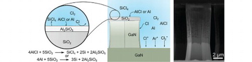
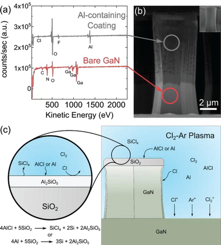
Previous experiments on deep etching GaN in an electron cyclotron resonance (ECR) plasma etcher resulted in anomalously high GaN:SiO2 etch selectivities of 39 [Citation23]. After etching in that system, the etched features were visibly coated with a residue as seen in the SEM image in Figure (b) which were revealed to be an Al-containing material by Auger electron spectroscopy (Figure (a)). The Al residue was easily removable by solvent or 3:1 H2SO4:H2O2, and a cleaned pillar is depicted in the inset of Figure (b). We determined that the likely source was the Al carrier plate. We also hypothesized that the Al residue was responsible for the increased selectivity by the mechanism depicted in Figure (c). Volatile AlCl or sputtered aluminum released from the plate is transported through the plasma to the GaN sample surfaces. When AlCl comes into contact with the SiO2 mask, the following reaction takes place to transform the SiO2 into Al2SiO5 [Citation24]:
(1)
(1)
If elemental Al contacts the SiO2 surface, then the following reaction can proceed:
(2)
(2)
Based on the values in the NIST-JANAF Thermochemical Tables, both reactions are strongly thermodynamically favorable. The Si in the product of these reactions can be easily etched by free Cl species in the plasma while pure Al2O3 is known to etch more slowly in a Cl2-Ar plasma [Citation25,Citation26]. For SiO2, etching is rate limited by the removal of O by physical sputtering [Citation27]. The threshold displacement energy for O in Al2O3 (∼75-80 eV) [Citation28–30] is much stronger than that of SiO2 (∼10–50 eV) [Citation31,Citation32] and therefore sputtering is expected to be lower for Al2O3 compared to SiO2. Although plasma etching of Al2SiO5 compounds are unexplored in the literature, since Al2SiO5 and other aluminum silicates are composed of Al2O3 and SiO2 polyhedra (the base building blocks of each compound), the etch rate may be expected to be between that of pure Al2O3 and SiO2 and be rate limited by etching of the Al2O3 polyhedra. Additionally, adding small amounts of O2 to Cl2-based plasmas results in high GaN:AlGaN selectivities as high as 68:1 through the formation of AlxOy compounds on the AlGaN surface [Citation33–36]. Thus, the reaction of Al or AlCl with the SiO2 surface is expected reduce the mask etch rate, and therefore increases the GaN:SiO2 selectivity. We believe that this is the cause of our anomalously high selectivity in our prior results.
Figure 1. Auger electron spectra (a) of a GaN pillar (b) etched in an electron cyclotron resonance (ECR) plasma etcher showing the presence of an Al-containing residue on the pillar after etching. Schematic of the mask hardening mechanism (c). Al-containing species in the plasma react with the SiO2 surface to form a robust, etch-resistant Al2SiO5 surface layer which enhances the effective GaN:SiO2 etch selectivity.
To test our hypothesis, we modulated the amount of Al entering a Cl2-Ar plasma in an inductively coupled plasma etcher while etching GaN. The introduction of Al to the plasma was done by placing the GaN chips onto carrier wafers of different Al-containing materials which etch incidentally in the plasma. OES of the plasma verifies the relative amounts of Al in the plasma (Figure ) when using the different carrier wafers. The sapphire releases a negligible amount of Al in the plasma as is indicated by only a small Al peak at 396 nm [Citation37] (note: OES of a fused silica wafer (not shown) produces a nearly identical spectrum with a small Al peak at 396 nm. Thus, the sapphire OES spectrum can be effectively taken as the background spectra of the Cl2-Ar plasma). The AlN wafer produces a strong AlCl signal at 261 nm [Citation38–40] and strong Al signals at 308 and 396 nm [Citation37] in the OES. The Al wafer has even stronger AlCl and Al peaks in the OES than the AlN indicating that it releases more Al species into the plasma. Thus, the relative amounts of Al containing-species in the plasma resulting from the carrier wafers is sapphire < AlN < Al.
Figure 2. Optical emission spectra of Cl2-Ar plasmas (25 W RF power) using sapphire, AlN, and Al carrier wafers. Based on the spectra, sapphire releases a negligible amount of free Al or AlCl into the plasma. While the AlN and Al release moderate and high amounts of Al and AlCl into the plasma, respectively.
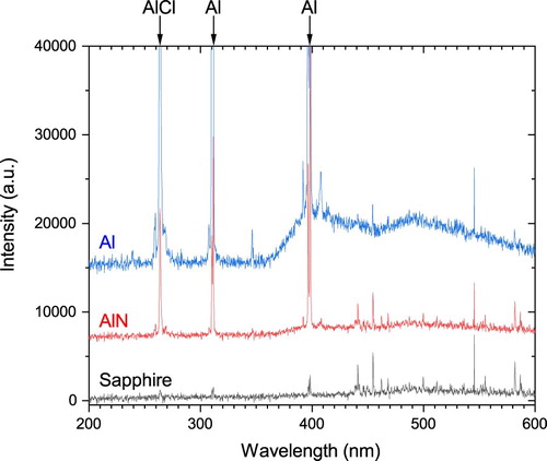
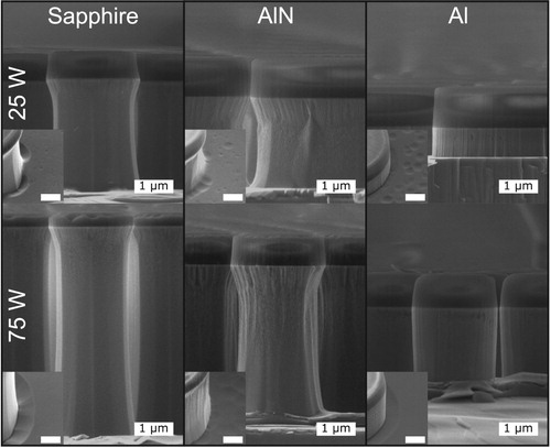
Figure shows the GaN and SiO2 etch rates, and the GaN:SiO2 etch selectivity for samples etched using each of the carrier wafers. Figure depicts cross-sectional SEM images of the etched GaN using the various carrier wafers, which highlights the significant impact of the carrier wafer and RF power conditions on the etch rates and surface morphology. The etch rates for both the GaN and the SiO2 are higher for the 75 W RF power condition (DC bias ≈ −205 V), as expected due to higher ion bombardment energy. At 25 W RF (DC bias ≈ −87 V), the etch rate is reduced by about a factor of six or more when using AlN and Al compared to sapphire. The lower GaN etch rate for AlN and Al may be due to sinking of the Cl2 in the plasma. Despite the lower GaN etch rates for these materials, the extremely low SiO2 etch rate results in much higher etch selectivities. These results support our hypothesis that Al species in the plasma are increasing the GaN:SiO2 etch rate by slowing the SiO2 etching. The carriers also have an effect on the surface morphology of the etched features. Trenching is influenced by the carriers and is present to some extent under each condition and can be seen in the insets in Figure . This phenomenon is a result of ions glancing off of the etched side walls and increasing the ion flux near the base of the etched features [Citation41]. Pitting is also observed on the etched floor, particularly under 25 W RF power. These etch pits are a result of defect selective etching and are more pronounced under a more chemically driven etch (lower ion energy) at 25 W RF.
Figure 3. GaN etch rates (a) SiO2 mask etch rates (b) and subsequent GaN:SiO2 etch selectivity (c) for the samples etched using different carrier wafer types at 25 and 75 W RF power. When AlN and Al carrier wafers are used, the SiO2 etch rate is drastically reduced, resulting in higher GaN:SiO2 etch selectivities compared to using the sapphire carrier wafer.
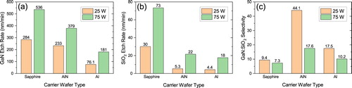
Figure 4. Scanning electron images of the etched GaN pillars using sapphire, AlN, and Al carrier wafers at 25 and 75 W RF power. The insets show the etched floor imaged at a 45° angle. The scale bar in the inset is 1 μm.
To confirm the presence of an Al2SiO5 layer on the surface of the SiO2 masks due to Al species in the etch plasma, AES was measured on the pillar tops (on the SiO2 mask), the pillar sidewall, and the etched floor. The compositions of the surfaces are shown in Figure . The mask of the sapphire sample is composed largely of Si and O, indicating that the surface is unmodified. In contrast, the mask surface of the AlN sample has a reduced Si concentration and is enriched in Al. The measured composition is Al0.28Si0.17O0.55, which is in reasonable agreement with the formula Al2SiO5. The lack of a strong Al signal on the etched floor indicates that the Al is indeed reacting with the SiO2 and is not easily sputtered from the surface. The Al carrier wafer coated all surfaces with an Al and C-rich material. The presence of Al on the mask likely results in a similar surface reaction with the SiO2, but such a layer would be obfuscated by the large amount of Al and C on the surface. The excessive coating of all of the surfaces explains the low GaN etch rate (the coating on the etched floor needs to be continuously removed to etch the GaN) and the vertical sidewall (the coating passivates the surface and prevents lateral etching of the GaN).
Figure 5. Scanning electron image of GaN pillar etched at 25 W RF power (a) and atomic surface composition of the pillar mask (b), pillar sidewall (c), and the etched floor (d) as measured by Auger electron spectroscopy. The surface composition of the mask reveals that Al released from the AlN carrier wafer reacts with the SiO2 to form an Al2SiO5 surface layer while the SiO2 surface for the sapphire carrier wafer remains as SiO2.
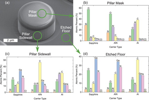
The surface composition of the SiO2 mask correlates with both the OES signal of Al in the plasma (Figure ) and the etch rate of the SiO2 (Figure ). When the sapphire carrier wafer is used, insignificant amounts of Al enter the plasma, and the SiO2 mask etch rate is unaffected. If either the AlN or Al carrier wafer is used, AlCl and Al are introduced into the plasma which can then react with the SiO2 to form a hardened Al2SiO5 surface layer which slows the mask etch rate and increases the GaN:SiO2 etch selectivity. Despite the etch resistance of the surface modified mask to the Cl2-Ar plasma, the masks are still easily removed by wet etching using buffered oxide etch (BOE) for 15 min, consistent with reports of atomic layer deposited Al2O3 [Citation42] and Al2SiO5 [Citation43].
For chip-level processing, using an etchable Al-containing carrier to introduce Al directly to the plasma is an easy and accessible way to increase GaN:SiO2 mask selectivity. However, as the chip size is increased and more of the carrier is covered, uniformity may become a concern as the Al needs to be transported from the carrier, into the plasma, and back to the GaN surface. Further, as less of the carrier is exposed to the plasma, less Al will be introduced to the plasma, and the process would be affected. Ultimately, to overcome these concerns, a more controllable method for introducing Al into the plasma should be pursued. This may be as simple as bleeding small amounts of an Al-containing gas such as AlCl, AlCl3 or trimethylaluminum (TMA) continuously into the plasma. These Al sources would then be treated as a process gas and the amount of Al in the plasma could be directly and independently controlled. Such a technique would provide a scalable method to take advantage of standard SiO2 deposition and patterning techniques with the benefit of having an etch-resistant aluminum-silicate hard mask.
Conclusions
We understand and have demonstrated drastically improved GaN:SiO2 etch selectivities in a Cl2-Ar plasma by introducing Al species into the plasma. The Al species react with the SiO2 surface to form an Al2SiO5 which is more etch resistant than pure SiO2. This effect provides a route to using SiO2 as a mask for deep etching of GaN without the contamination or patterning concerns that using metal masks entail.
Acknowledgements
This work was performed under the auspices of the U.S. Department of Energy by Lawrence Livermore National Laboratory under Contract DE-AC52-07NA27344, LDRD Tracking #19-FS-005, LLNL-JRNL-809923.
Disclosure statement
No potential conflict of interest was reported by the author(s).
Additional information
Funding
References
- Hassan A, Savaria Y, Sawan M. Gan integration technology, an ideal candidate for high-temperature applications: a review. IEEE Access. 2018 Dec 7;6:78790–78802.
- Ahi K. Review of GaN-based devices for terahertz operation. Opt Eng. 2017 Sep;56(9):090901:1-14.
- Jones EA, Wang FF, Costinett D. Review of commercial GaN power devices and GaN-based converter design challenges. IEEE J Emerg Sel Top Power Electron. 2016 Jun 21;4(3):707–719.
- Moustakas TD, Paiella R. Optoelectronic device physics and technology of nitride semiconductors from the UV to the terahertz. Rep Prog Phys. 2017 Sep 1;80(10):106501:1-41.
- Zhang Y, Sun M, Piedra D, et al. 1200 V GaN vertical fin power field-effect transistors. In 2017 IEEE Int Electron Devices Meet. (IEDM) 2017 Dec 2-6; San Francisco, California (pp. 9-2). IEEE.
- Wang H, Xiao M, Sheng K, et al. Switching performance analysis of vertical GaN FinFETs: impact of inter-fin designs. IEEE J Emerg Sel Top Power Electron. 2020 Mar 12.
- Zhang Y, Dadgar A, Palacios T. Gallium nitride vertical power devices on foreign substrates: a review and outlook. J Phys D Appl Phys. 2018 Jun 12;51(27):273001:1-13.
- Kotzea S, Debald A, Heuken M, et al. Demonstration of a GaN-based vertical-channel JFET fabricated by selective-area regrowth. IEEE Trans Electron Devices. 2018 Oct 26;65(12):5329–5336.
- Liu C, Khadar RA, Matioli E. Vertical GaN-on-Si MOSFETs with monolithically integrated freewheeling Schottky barrier diodes. IEEE Electron Device Lett. 2018 Jun 1;39(7):1034–1037.
- Ma Y, Xiao M, Zhang R, et al. Superjunction power transistors with interface charges: a case study for GaN. IEEE J Electron Devices Soc. 2019 Dec 13;8:42–48.
- Xiao M, Zhang R, Dong D, et al. Design and simulation of GaN superjunction transistors with 2-DEG channels and fin channels. IEEE J Emerg Sel Top Power Electron. 2019 Apr 24;7(3):1475–1484.
- Zhu C, Zhou X, Feng Z, et al. Theoretical investigation of high-voltage superjunction GaN-based vertical hetero-junction field effect transistor with ununiformly doped buffer to suppress charge imbalance effect. Semicond Sci Technol. 2019 May 22;34(6):065012:1-8.
- Zhuang D, Edgar JH. Wet etching of GaN, AlN, and SiC: a review. Mater Sci Eng R Rep. 2005 Jan 17;48(1):1–46.
- Pearton SJ, Douglas EA, Shul RJ, et al. Plasma etching of wide bandgap and ultrawide bandgap semiconductors. J Vac Sci Technol A. 2020 Mar 16;38(2):020802:1-15.
- Ladroue J, Meritan A, Boufnichel M, et al. Deep GaN etching by inductively coupled plasma and induced surface defects. J Vac Sci Technol A. 2010 Sep 3;28(5):1226–1233.
- Shields P, Hugues M, Zúñiga-Pérez J, et al. Fabrication and properties of etched GaN nanorods. Phys Status Solidi c. 2012 Mar;9(3-4):631–634.
- Hahn H, Gruis JB, Ketteniss N, et al. Influence of mask material and process parameters on etch angle in a chlorine-based GaN dry etch. J Vac Sci Technol A. 2012 Sep 20;30(5):051302:1-5.
- Le Boulbar ED, Lewins CJ, Allsopp DW, et al. Fabrication of high-aspect ratio GaN nanostructures for advanced photonic devices. Microelectron Eng. 2016 Mar 5;153:132–136.
- Chang LB, Liu SS, Jeng MJ. Etching selectivity and surface profile of GaN in the Ni, SiO2 and photoresist masks using an inductively coupled plasma. Jpn J Appl Phys. 2001 Mar;40(3R):1242:1242–1243.
- Claeys C, Simoen E. Device performance as a metrology tool to detect metals in silicon. Phys Status Solidi (a). 2019 Sep;216(17):1900126:1-10.
- Tahhan M, Nedy J, Chan SH, et al. Optimization of a chlorine-based deep vertical etch of GaN demonstrating low damage and low roughness. J Vac Sci Technol A. 2016 May 15;34(3):031303:1-6.
- Shul RJ, Pearton SJ, editors. Handbook of advanced plasma processing techniques. Springer Science & Business Media [Berlin]; 2011 Jun 28.
- Harrison SE, Voss LF, Torres AM, et al. Ultradeep electron cyclotron resonance plasma etching of GaN. J Vac Sci Technol A. 2017 Nov 25;35(6):061303:1-7.
- Kumagai Y, Yamane T, Miyaji T, et al. Hydride vapor phase epitaxy of AlN: thermodynamic analysis of aluminum source and its application to growth. Phys Status Solidi (c). 2003 Dec; 0(7):2498–2501.
- Koo SM, Kim DP, Kim KT, et al. The etching properties of Al2O3 thin films in N2/Cl2/BCl3 and Ar/Cl2/BCl3 gas chemistry. Mater Sci Eng B Solid State Mater Adv Technol. 2005 Apr 25;118(1-3):201–204.
- Bradley JD, Ay F, Wörhoff K, et al. Fabrication of low-loss channel waveguides in Al2O3 and Y2O3 layers by inductively coupled plasma reactive ion etching. Appl Phys B. 2007 Nov 1;89(2-3):311–318.
- Chang JP, Sawin HH. Molecular-beam study of the plasma-surface kinetics of silicon dioxide and photoresist etching with chlorine. J Vac Sci Technol B Nanotechnol Microelectron. 2001 Jul;19(4):1319–1327.
- Agnew P. Displacement thresholds in sapphire. Philos Mag A. 1992 Feb 1;65(2):355–361.
- Pells GP, Phillips DC. Radiation damage of α-Al2O3 in the HVEM: I. temperature dependence of the displacement threshold. J Nucl Mater. 1979 May 1;80(2):207–214.
- Pells GP, Phillips DC. Radiation damage of α-Al2O3 in the HVEM: II. Radiation damage at high temperature and high dose. J Nucl Mater. 1979 May 1;80(2):215–222.
- Pfeffer RL. Damage center formation in SiO2 thin films by fast electron irradiation. J Appl Phys. 1985 Jun 15;57(12):5176–5180.
- Arnold GW. Defect structure of crystalline quartz. II. Variation of displacement threshold energy with crystal growth rate. Phys Rev. 1965 Oct 4;140(1A):A176-A178.
- Wong JC, Micovic M, Brown DF, et al. Selective anisotropic etching of GaN over AlGaN for very thin films. J Vac Sci Technol A. 2018 May 20;36(3):030603:1–5.
- Han Y, Xue S, Guo W, et al. Highly selective dry etching of GaN over AlGaN using inductively coupled Cl2/N2/O2 plasmas. Jpn J Appl Phys. 2003 Sep 25;42(10A):L1139-L1141.
- Lee YH, Sung YJ, Yeom GY, et al. Magnetized inductively coupled plasma etching of GaN in Cl2/BCl3 plasmas. J Vac Sci Technol A. 2000 Jul;18(4):1390–1394.
- Buttari D, Chini A, Palacios T, et al. Origin of etch delay time in Cl2 dry etching of AlGaN/GaN structures. Appl Phys Lett. 2003 Dec 8;83(23):4779–4781.
- Sansonetti JE, Martin WC. Handbook of basic atomic spectroscopic data. J Phys Chem Ref Data. 2005 Dec 28;34(4):1559–2259.
- Bhaduri BN, Fowler A. Band spectrum of aluminium chloride (AlCl). Proc R Soc Lond A Math Phys Sci. 1934 Jun 2;145(854):321–336.
- Foster LM, Russell AS, Cochran CN. Spectroscopic investigation of the reaction between aluminum and aluminum chloride. J ACS. 1950 Jun;72(6):2580–2587.
- Zheng J, Sun B, Yang R, et al. Metal Al produced by H2 plasma reduction of AlCl3: a thermodynamic and kinetic study on the plasma chemistry. J Phys Chem B. 2008 Oct 9;112(40):12748–12752.
- Van Nguyen S, Dobuzinsky D, Stiffler SR, et al. Substrate trenching mechanism during plasma and magnetically enhanced polysilicon etching. J Electrochem Soc. 1991 Apr 1;138(4):1112-1117.
- Puurunen RL, Saarilahti J, Kattelus H. Implementing ALD layers in MEMS processing. ECS Trans. 2007 Sep 28;11(7):3-14.
- Lim JW, Yun SJ, Lee JH. Characteristics of aluminum silicate films grown by plasma-enhanced atomic layer deposition. Electrochem Solid State Lett. 2005 Jul 18;8(9):F25-F28.