
Abstract
In this work, we use in-situ TEM in combination with finite elemental analysis to reveal the sub-grain boundary formation during bending of Cu single crystal. The deformation process is featured by dislocations propagation, formation of stacking faults and deformation twins, and subsequent formation of a sub-grain boundary. Finite element analysis of stress distribution indicates the stacking faults and deformation twins are all initiated from the region that corresponds to the maximum shear stress. The formation of the sub-grain boundary is through the intersection between primary and secondary stacking faults/deformation twins.
GRAPHICAL ABSTRACT
IMPACT STATEMENT
Real-time observation of the plastic deformation process during the bending of Cu single crystal, reveals the sub-grain boundary formation through the intersection between primary and secondary stacking faults/deformation twins.
Introduction
Plastic deformation at large strain induces pumped up of dislocation density by orders of magnitude and correspondingly microstructure evolution that is featured by grain refinement, resulting in excellent mechanical properties in metals and alloys [Citation1–3]. Various severe plastic deformation (SPD) techniques have been developed to enhance the properties of metallic materials, such as high-pressure torsion, equal channel angular pressing, and accumulative roll-bonding [Citation4, Citation5].
In the last decades, extensive efforts have been devoted to understand the SPD induced grain refinement with numerous sub-grain and grain boundary formations [Citation4, Citation6–8]. Two well-accepted mechanisms have been proposed to account for the grain refinement process. One is the dislocation activities dominated mechanism, including dislocation nucleation and multiplication, accumulation, interaction, tangling and spatial rearrangement[Citation9–11], which is well documented for metallic materials with medium and high stacking fault energy (SFE) deformed at conventional strain rates and ambient temperature. During deformation, each coarse grain is divided into cell blocks and cells with cell boundaries formed by dislocations. Some cell boundaries transformed into sub-grain boundaries with small misorientations. With increasing strain, some neighboring cell blocks with increased misorientations become high-angle (above 15°) grain boundaries eventually, which result in the formation of smaller grains inside the initial coarse grains. The other mechanism is dominated by deformation twinning, which normally occurs in hexagonal close-packed (hcp) as well as body-centered cubic (bcc) /face-centered cubic(fcc) metallic materials with low SFEs, especially at high strain rate and low temperatures as dislocation slips are effectively suppressed [Citation12–14]. Based on microstructure observations in various fcc metals under deformation, different mechanisms have been identified for the deformation twinning dominated refinement due to SFE, grain size, strain, strain rate, and temperature, such as fragmentation of twin/matrix (T/M) lamellae where the dislocations accumulated within T/M layers or at twin boundaries (TBs) to fragment lamellae into refining grains [Citation12, Citation15], formation of secondary twins subdividing the lamellae into prismatic nanosized blocks [Citation16], twin-twin intersection dividing two sets of T/M lamellae into rhomboid blocks [Citation16, Citation17], shearing banding of T/M lamellae with equiaxed nanosized grains [Citation15]. In addition, the grain boundary (GB) mediated mechanisms, such as grain rotation and GB-sliding, may play significant roles when the grain size comes to nano scale [Citation3]. For the fcc metals with medium SFE (such as Cu, ∼78mJ/m2 [Citation18, Citation19]), sub-grain boundary formation is considered to be associated with deformation twinning in material featured by nanometer grain size, while dominated by dislocation activities for micrometer grain size [Citation12, Citation13, Citation20].
However, due to most of these investigations about microstructural changes focused on the late or steady-state stages, there is a lack of knowledge about critical information governing dynamic deformation. In-situ transmission electron microscopy (TEM) observation with mechanical testing, as has already demonstrated with various deformation behavior with crystal defects, such as dislocation glide [Citation21–23], (de)twinning [Citation23–28], and GB migration [Citation29–31], provides powerful approaches to unravel the mystery of dynamic deformation process [Citation32, Citation33]. So far, the understanding of the dynamic GB formation process induced by plastic deformation [Citation34] is very limited, especially in materials with micron-grain size which is generally used for SPD instead of the nanocrystal.
In this work, we investigate shear strain induced sub-grain boundary formation during in-situ TEM bending of Cu single crystal specimen with micron size. The deformation process is featured by dislocations propagation, stacking faults (SFs) and deformation twins (DTs) nucleation, and finally sub-grain boundary formation. Combining the finite element analysis of stress distribution inside the specimen under bending, the SFs and DTs all generate from the free surface and the inner region where the shear strain is the maximum. Therefore, the shear strain is considered to be the primary cause for the SFs and DTs nucleation. In addition, we confirm the intersections between primary and secondary SFs/DTs induce the sub-grain boundary formation.
Experimental methods
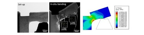
The sample for in-situ mechanical testing was fabricated from 99.99% pure Cu single crystal by the focused ion beam (FIB) technique using a Helios Dual Beam instrument. A ∼ 2 μm thick cube was mounted on a Cu grid. Subsequent thinning processes were performed, and the specific sample geometry was shaped by using the ion beam of 5 kV/16pA to minimize the damage. Bright-field (BF)-TEM image of the as-fabricated sample is shown in Figure (b). The left-top of the fixed part is cut to allow more displacement and deformation of the sample before fracture. The thickness of the cantilever is about 300 nm to avoid buckling of the sample during bending. Selected area electron diffraction (SAED) indicates the projection direction of the sample is near the <011 > axis of Cu.
Figure 1. (a) Schematics illustrating the in-situ bending set-up. (b)The bright-field TEM image shows the as-fabricated Cu single crystal sample touched by the tungsten indenter. The insert selected electron diffraction indicates the sample has the near [011] projection direction. (c, d) The snapshots with dark-field TEM imaging mode of the area marked by the black dash line in (b) during the initial bending stage, show the SF generated from the free surface of the specimen. The white dash line represents the free surface. (e) The shear stress (MPa) distribution in the specimen under the initial bending stage was obtained from finite element analysis. (f-h) The following sequential snapshots show the SF growth and broaden to form DT, as well as some SFs generated from both free surface and inner of the specimen.
![Figure 1. (a) Schematics illustrating the in-situ bending set-up. (b)The bright-field TEM image shows the as-fabricated Cu single crystal sample touched by the tungsten indenter. The insert selected electron diffraction indicates the sample has the near [011] projection direction. (c, d) The snapshots with dark-field TEM imaging mode of the area marked by the black dash line in (b) during the initial bending stage, show the SF generated from the free surface of the specimen. The white dash line represents the free surface. (e) The shear stress (MPa) distribution in the specimen under the initial bending stage was obtained from finite element analysis. (f-h) The following sequential snapshots show the SF growth and broaden to form DT, as well as some SFs generated from both free surface and inner of the specimen.](/cms/asset/35ba4b57-082d-46b4-be28-3cb3b0a2c5f5/tmrl_a_2057201_f0001_oc.jpg)
The in-situ bending was operated in FEI 80–300 Titan equipped with an imaging aberration corrector by using a Nanofactory holder. The in-situ set-up is shown in Figure (a,b), where the in-situ bending was carried out by moving the tungsten indenter forward with a constant speed of about 1 nm s−1. All videos were recorded in real-time by a charge-coupled device (CCD) camera at a rate of 0.2 s per frame. The Supplementary Videos 2, 4, and 5 are played at 5, 5,10 times of recording frame rate, respectively. Three-dimensional finite element analysis was carried out using the commercial software ABAQUSTM to reveal the stress distribution in the specimen under in-situ bending.
Results and discussion
During the initial bending process, the formation and growth of SFs occurred at the area with maximum shear stress, and some of the SFs integrated to form DTs. As shown in Figure (c), the Cu single crystal specimen contains a high density of dislocations even before deformation. These pre-existing dislocations may come from two sources. One is the dislocations originally existed in the single crystal, while the other one is the dislocations induced by the FIB milling process. The dislocations induced by FIB milling should not affect the mechanical behavior of the specimen since they only generate at the surface region less than 10 nm deepness with 5 kV/16pA ion beam [Citation35]. Figure (d) shows the first SF initiates from the free surface. The slight contrast changes in Supplementary Video S1 indicate dislocation propagation during deformation. As visible from the Supplementary Video S1, the SF grows inside very quickly as soon as it is nucleated, therefore it is hard to differentiate the nucleation and the subsequent growth process. However, the SF will be trapped by the increasing Peierls-Nabarro stress (lattice resistance to dislocation motion) [Citation36, Citation37] or other dislocations when it is growing inside, leading to the case of a segment of SF (Figure (d)), instead of crossing the whole specimen. Combining the shear stress distribution in the specimen obtained from finite element analysis (Figure (e)), the SF is found to initiate from the free surface region where the shear stress is calculated to be the maximum. It implies that shear strain plays an important role in the nucleation of SF. With the increasing bending, SFs are continuously generated from the shear stress concentrated region, as shown in Figure (f–h). Furthermore, by absorbing other SFs on the adjacent slip plane, an SF could gain thickness to form DT. This dynamic DT formation process can be clearly observed in Supplementary Video S2. The enlarged DT in Figure (h) shows two needles at the head, which indicates the constituent SFs have different growth speeds. Meanwhile, along with the increasing bending, the SFs generated from within the crystal, instead of the free surface, also have been observed. Combining the finite element analysis and experimental results, it is clear that SFs and DTs are both first generated in the region with maximum shear stress either free surface or within the crystal. Besides the generation of SFs and DTs, the annihilation of SF also has been observed during in-situ bending (Supplementary Video S3). Generally, the SF segment is formed by the gliding of leading Shockley partial dislocation. The SF existed until another trailing Shockley partial dislocation emitted and glided along the same slip plane with the erasure of the SF. This deformation behavior will induce a full dislocation inside the specimen, which is a common defects reaction inside fcc metals with low/medium SFEs [Citation30, Citation38–40]. The observation that both the formation and annihilation of SF occur within a short period (∼ one second) appears to be consistent with the previous observation that the gliding of partial dislocation is very quick after the nucleation [Citation41, Citation42].
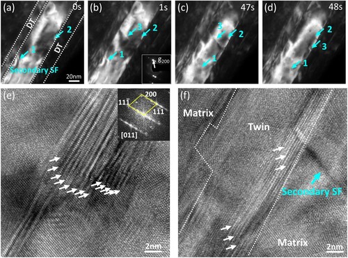
The SFs and DTs formed in the initial deformation all have the same (11-1) slip plane, named as the primary slip plane for easy description. Along with the increasing bending, SF lying on the (1-11) slip plane (named as secondary slip plane) nucleates within the matrix lamellas (Figure and Supplementary Video S4). As shown in Figure (a) (set as 0s), SF segments generate from the twin boundary (TB) and are arrested within the matrix lamellae. One second later (Figure (b)), another SF nucleates and grows across the whole lamella (marked as ‘3’). Formation of SF ‘3’ should be induced by a leading Shockley partial dislocation generated at the TB, which subsequently glides across the lamellae to stop at the other TB. This SF ‘3’ stays stable for a while (Figure (c)), until the trailing partial dislocation generates and glides across the twin lamellae, which erasure the SF and left a full dislocation at the TB (Figure (d)). Meanwhile, the SF marked as 1 and 2 remain intact, likely indicating that the accumulated elastic energy is not large enough to surpass the barrier that traps their leading partial dislocations. Figure (e) shows the tip region of one DT, which contains a high density of SFs accompanied by partial dislocations, demonstrated by the streaking feature of the FFT. The TBs in Figure (f) also show a similar feature with a high density of SFs and contain some steps instead of completely straight. These results imply that DTs can grow wide by consolidating other SFs. The dark-field and high-resolution TEM images in Figure both confirm the SF with secondary slip system activated at the TB in the matrix lamellae, which is also consistent with previous reports [Citation39, Citation43, Citation44]. These observations demonstrate that the increasing bending induces activation of the secondary slip system and the formation of a 2D SF network inside the specimen, leading to the work hardening of the material.
Figure 2. (a-d) The sequential snapshots with dark-field TEM imaging mode show the nucleation and annihilation of one SF with the secondary (11-1) slip plane (marked as 3) inside matrix lamellae. There are other inactive SFs inside the matrix lamellae marked as 1 and 2. The dash lines in (a) indicate the deformation twin (DT). The insert in (b) indicates the dark-field images are under g = 200. The high-resolution TEM images of (e) the tip region of DT and (f) the DT lamellae. The insert in (e) shows the FFT. The white and cyanic arrows indicate the SFs with primary slip system and secondary slip system, respectively. The TBs are marked by dash lines in (a,f).
Besides the small SF generated inside the matrix/twin lamellae, an SF segment lying on the secondary slip plane formed in front of primary DTs as shown in Figure (a). With increasing deformation, this SF acts as a boundary to block the continued growth of all the primary DTs (Figure (b–d) and Supplementary video S5). Meanwhile, the TBs of primary DTs could act as easy slip planes for dislocation sliding, resulting in dislocations accumulation beside the secondary SF. At the end stage of the deformation, the SF with the secondary slip plane, which acted as a blocked boundary for primary DTs, evolved into a sub-grain boundary, as demonstrated in Figure . The specimen surface is rotated about 30° due to large bending deformation (Figure (a)). The SAED (Figure (b–d)) indicates the orientations of two regions besides the sub-grain boundary are near the [1-2-3] and [1-1-2] of Cu phase, respectively. The corresponding finite element analysis of shear stress distribution in the specimen (Figure (e)) implies the primary DTs generate at the region with maximal shear stress and are trapped by sub-grain boundary formed at the region with medium shear stress.
Figure 3. (a) The snapshots with dark-field TEM imaging mode showing the 2D SF network. The SF generated in front of the primary DTs is marked by the cyanic arrows. (b-d) The sequential snapshots show the SF stays stable and acts as a boundary blocking the growth of DTs during the increasing bending deformation. The dash lines represent the initial position of boundary and free surface in (b).
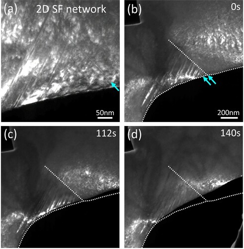
Figure 4. (a) The dark-field TEM image of the specimen at the end stage of in-situ bending. (b) The enlarged image of the region is marked by a blue rectangle in (a), where the boundary is indicated by a white dash line. (c, d) The corresponding selected area electron diffraction patterns of the areas marked 1 and 2 in (b), represent the nearly [1-2-3] and [1-1-2] projection direction, respectively. (e) The shear stress (MPa) distribution in the specimen at the end stage of the in-situ bending was obtained from finite element analysis. (f) The standard stereographic triangle of face-centered cubic crystal, showing the rotation angle between the different orientations.
![Figure 4. (a) The dark-field TEM image of the specimen at the end stage of in-situ bending. (b) The enlarged image of the region is marked by a blue rectangle in (a), where the boundary is indicated by a white dash line. (c, d) The corresponding selected area electron diffraction patterns of the areas marked 1 and 2 in (b), represent the nearly [1-2-3] and [1-1-2] projection direction, respectively. (e) The shear stress (MPa) distribution in the specimen at the end stage of the in-situ bending was obtained from finite element analysis. (f) The standard stereographic triangle of face-centered cubic crystal, showing the rotation angle between the different orientations.](/cms/asset/c14fd6cc-e7c7-46d4-ac85-ba59b03a1bf8/tmrl_a_2057201_f0004_oc.jpg)
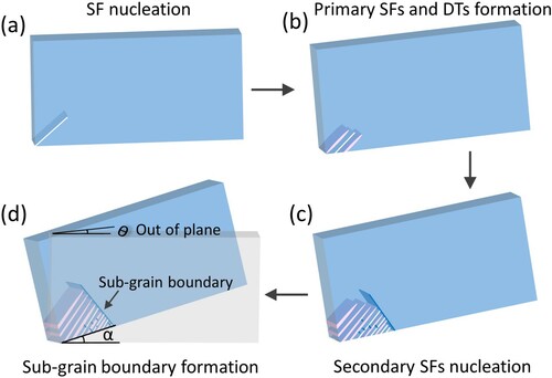
According to the standard stereographic triangle of face-centered cubic crystal (Figure (f)), the boundary observed in the specimen after bending is confirmed to be a sub-grain boundary with misorientation angles between [1-2-3] and [1-1-2] axis of Cu phase (about 10.9°). In addition, the width of the specimen decreased from 2.85 μm to 2.72 μm after the bending, indicating the out-of-plane rigid rotation is about 17.4°. This angle is near the rotation angle between the [1-2-3] and [011] orientation (19.1° in Figure (f)). It confirms the specimen rotated along out-of-plane to accomplish the reorientation from the initial [011] to [1-2-3], consistent with the SAED result of region 1 in Figure (c). While the rotation of region 2 from [1-2-3] to [1-1-2] is accomplished by the nucleation and accumulation of crystal defects including dislocations, SFs, and DTs. To sum up, the rotation of specimen surface (30°) represents the total geometric rotation caused by in-situ bending, which is accommodated through two processes. One is the rigid rotation of about 17.4° along the out-of-plane leading to the reorientation from [011] to [1-2-3]. The other one is the defects induced plastic deformation with a sub-grain boundary formation leading to the reorientation from [1-2-3] to [1-1-2]. During this bending induced plastic deformation, the defects generation and microstructure evolution follow the sequence as schematically illustrated in Figure . At first, shear stress induced dislocations and SFs nucleation at the free surface (Figure (a)). Subsequently, with increasing deformation, the SFs propagation and DTs formation occur (Figure (b)). During the inward propagation, the DTs narrow down is noticed due to some of the twinning partial dislocations being arrested. Then, the second slip system is activated with some SFs nucleation inside matrix/twin lamellas, as well as an SF with the secondary slip system generated at the head of primary DTs (Figure (c)). This secondary SF pin in front of primary DTs acts as a barrier to block the primary DT propagation, induces dislocation accumulation, and finally evolves into a sub-grain boundary (Figure (d)). The sub-grain boundary formation process is different from the dislocation dominated mechanisms in coarse-grained Cu or conventional DT dominated mechanisms in nanocrystalline Cu. The nanometer scale thickness (300 nm) of the specimen compared to the micron sized in-plane dimension will lead to a decreased critical shear stress for SFs/twins emission, contributing to the SFs/DTs generation. We believe the deformation twin induced sub-grain boundary formation mechanism should be widely applicable to explain the grain refinement of fcc metals with medium SFEs and grain size (a few hundred nanometers to 1 micrometer) under SPD.
Figure 5. The schematics show the microstructure evolution during the sub-grain boundary formation process in the specimen under in-situ bending. The primary SFs, DTs and secondary SFs are marked by white, pink and blue colors, respectively.
Conclusion
By performing the in-situ bending on a Cu single crystal specimen with micron size inside TEM, we captured the plastic deformation induced sub-grain boundary formation. The deformation process follows the sequence as (i) accompanied by dislocations propagation, primary SFs and DTs nucleate at the region with maximal shear stress; (ii) Secondary SFs generate inside matrix/twin lamellae as well as in front of the primary DTs; (iii) The secondary SF acts as a boundary to block the growth of primary twin and accumulate dislocations, which eventually evolves to a sub-grain boundary with misorientation about 11°. Combining the finite element analysis of stress distribution, we believe the shear strain is the primary cause for their formation. In addition, the dynamic observation indicates the sub-grain boundary is produced by the intersection between primary and secondary SFs/DTs. The in-situ TEM observation provides key insight for understanding the mechanism of sub-grain boundary formation associated with SFs and DTs under bending testing.
Supplemental Material
Download Zip (12.3 MB)Acknowledgement
This work was supported by the Laboratory Directed Research and Development program at Pacific Northwest National Laboratory (PNNL) as part of the Solid Phase Processing Science initiative. A portion of this research was performed using facilities at the Environmental Molecular Sciences Laboratory, a national scientific user facility sponsored by the U.S. Department of Energy’s (DOE’s) Office of Biological and Environmental Research and located at PNNL. PNNL is a multiprogram national laboratory operated by Battelle for the DOE under Contract DEAC05-76RL01830.
Funding
This work was supported by U.S. Department of Energy: [Grant Number DEAC05-76RL01830].
Disclosure statement
No potential conflict of interest was reported by the author(s).
References
- Liu XC, Zhang HW, Lu K. Strain-induced ultrahard and ultrastable nanolaminated structure in nickel. Science. 2013;342(6156):337–340.
- Piotrowski L, Chmielewski M, Kowalewski ZL. The dominant influence of plastic deformation induced residual stress on the barkhausen effect signal in martensitic steels. J Nondestr Eval. 2017;36(1.
- Cao Y, Ni S, Liao X, et al. Structural evolutions of metallic materials processed by severe plastic deformation. Mater Sci Eng: R: Rep. 2018;133:1–59.
- Valiev RZ, Islamgaliev RK, Alexandrov IV. Bulk nanostructured materials from severe plastic deformation. Prog Mater Sci. 2000;45(2):103–189.
- Estrin Y, Vinogradov A. Extreme grain refinement by severe plastic deformation: A wealth of challenging science. Acta Mater. 2013;61(3):782–817.
- Zhao YH, Zhu YT, Liao XZ, et al. Influence of stacking fault energy on the minimum grain size achieved in severe plastic deformation. Mater Sci Eng A. 2007;463(1-2):22–26.
- Zhao YH, Horita Z, Langdon TG, et al. Evolution of defect structures during cold rolling of ultrafine-grained Cu and Cu–Zn alloys: Influence of stacking fault energy. Mater Sci Eng A. 2008;474(1-2):342–347.
- Zhao YH, Liao XZ, Zhu YT, et al. Influence of stacking fault energy on nanostructure formation under high pressure torsion. Mater Sci Eng A. 2005;410-411:188–193.
- Hughes DA, Hansen N. High angle boundaries formed by grain subdivision mechanisms. Acta Mater. 1997;45(9):3871–3886.
- Liao XZ, Huang JY, Zhu YT, et al. Nanostructures and deformation mechanisms in a cryogenically ball-milled Al-Mg alloy. Philos Mag. 2003;83(26):3065–3075.
- Mishra A, Kad B, Gregori F, et al. Microstructural evolution in copper subjected to severe plastic deformation: experiments and analysis. Acta Mater. 2007;55(1):13–28.
- Wang K, Tao NR, Liu G, et al. Plastic strain-induced grain refinement at the nanometer scale in copper. Acta Mater. 2006;54(19):5281–5291.
- Tao NR, Lu K. Nanoscale structural refinement via deformation twinning in face-centered cubic metals. Scr Mater. 2009;60(12):1039–1043.
- Wang YB, Liao XZ, Zhao YH, et al. The role of stacking faults and twin boundaries in grain refinement of a Cu–Zn alloy processed by high-pressure torsion. Mater Sci Eng A. 2010;527(18-19):4959–4966.
- Li YS, Tao NR, Lu K. Microstructural evolution and nanostructure formation in copper during dynamic plastic deformation at cryogenic temperatures. Acta Mater. 2008;56(2):230–241.
- Zhang HW, Hei ZK, Liu G, et al. Formation of nanostructured surface layer on AISI 304 stainless steel by means of surface mechanical attrition treatment. Acta Mater. 2003;51(7):1871–1881.
- Wu X, Tao N, Hong Y, et al. Strain-induced grain refinement of cobalt during surface mechanical attrition treatment. Acta Mater. 2005;53(3):681–691.
- Loretto MH, Clarebrough LM, Segall RL. Stacking-fault tetrahedra in deformed face-centred cubic metals. Philos Mag. 1965;11(111):459–465.
- Zhao YH, Zhu YT, Liao XZ, et al. Tailoring stacking fault energy for high ductility and high strength in ultrafine grained Cu and its alloy. Appl Phys Lett. 2006;89(12).
- Huang CX, Wang K, Wu SD, et al. Deformation twinning in polycrystalline copper at room temperature and low strain rate. Acta Mater. 2006;54(3):655–665.
- Oh SH, Legros M, Kiener D, et al. In situ TEM straining of single crystal Au films on polyimide: change of deformation mechanisms at the nanoscale. Acta Mater. 2007;55(16):5558–5571.
- Zhou H, Huang C, Sha X, et al. In-situobservation of dislocation dynamics near heterostructured interfaces. Mater Res Lett. 2019;7(9):376–382.
- Ding Q, Fu X, Chen D, et al. Real-time nanoscale observation of deformation mechanisms in CrCoNi-based medium- to high-entropy alloys at cryogenic temperatures. Mater Today. 2019;25:21–27.
- Jang D, Li XH, Gao, et al. Deformation mechanisms in nanotwinned metal nanopillars, Nat Nanotechnol (2012);7(9):594-601.
- Cheng G, Yin S, Li C, et al. In-situ TEM study of dislocation interaction with twin boundary and retraction in twinned metallic nanowires. Acta Mater. 2020;196:304–312.
- Liu B-Y, Prasad KE, Yang N, et al. In-situ quantitative TEM investigation on the dynamic evolution of individual twin boundary in magnesium under cyclic loading. Acta Mater. 2019;179:414–423.
- Wang J, Li N, Anderoglu O, et al. Detwinning mechanisms for growth twins in face-centered cubic metals. Acta Mater. 2010;58(6):2262–2270.
- Zhu Q, Kong L, Lu H, et al. Revealing extreme twin-boundary shear deformability in metallic nanocrystals. Sci Adv. 2021;7(36):eabe4758.
- Zhu Q, Cao G, Wang J, et al. In situ atomistic observation of disconnection-mediated grain boundary migration. Nat Commun. 2019;10(1):156.
- Zhu Q, Huang Q, Guang C, et al. Metallic nanocrystals with low angle grain boundary for controllable plastic reversibility. Nat Commun. 2020;11(1):3100.
- Huang Q, Zhu Q, Chen Y, et al. Twinning-assisted dynamic adjustment of grain boundary mobility. Nat Commun. 2021;12(1):6695.
- Legros M. In situ mechanical TEM: seeing and measuring under stress with electrons. C R Phys. 2014;15(2-3):224–240.
- Kacher J, Zhu T, Pierron O, et al. Integrating in situ TEM experiments and atomistic simulations for defect mechanics. Curr Opin Solid State Mater Sci. 2019;23(3):117–128.
- Wang L, Kong D, Zhang Y, et al. Mechanically driven grain boundary formation in nickel nanowires. ACS Nano. 2017;11(12):12500–12508.
- Kiener D, Motz C, Rester M, et al. FIB damage of Cu and possible consequences for miniaturized mechanical tests. Mater Sci Eng A. 2007;459(1-2):262–272.
- Joós B, Duesbery MS. The peierls stress of dislocations: An analytic formula. Phys Rev Lett. 1997;78(2):266–269.
- Nabarro FRN. Fifty-year study of the peierls-nabarro stress. Mater Sci Eng A. 1997;234-236:67–76.
- Zheng H, Wang J, Huang JY, et al. In situ visualization of birth and annihilation of grain boundaries in an Au nanocrystal. Phys Rev Lett. 2012;109(22):225501.
- Li N, Wang J, Misra A, et al. Twinning dislocation multiplication at a coherent twin boundary. Acta Mater. 2011;59(15):5989–5996.
- Yamakov V, Wolf D, Phillpot SR, et al. Dislocation processes in the deformation of nanocrystalline aluminium by molecular-dynamics simulation. Nat Mater. 2002;1(1):45–48.
- Li S, Olszta M, Li L, et al. In-situ TEM observation of shear induced microstructure evolution in Cu-Nb alloy. Scr Mater. 2021;205:114214.
- Yue Y, Liu P, Deng Q, et al. Quantitative evidence of crossover toward partial dislocation mediated plasticity in copper single crystalline nanowires. Nano Lett. 2012;12(8):4045–4049.
- Lu K, Lu L, Suresh S. Strengthening materials by engineering coherent internal boundaries at the nanoscale. Science. 2009;324(5925):349–352.
- Dao M, Lu L, Shen YF, et al. Strength, strain-rate sensitivity and ductility of copper with nanoscale twins. Acta Mater. 2006;54(20):5421–5432.