
 ?Mathematical formulae have been encoded as MathML and are displayed in this HTML version using MathJax in order to improve their display. Uncheck the box to turn MathJax off. This feature requires Javascript. Click on a formula to zoom.
Abstract
Local thickening, resulting from displacive or diffusive mechanisms individually, is frequently observed in nanoscale metals during compression. However, it is not fully understood how a coupled displacive-diffusive mechanism would mediate the compressive deformation of metallic nanocrystal. Here, by conducting in situ atomic-scale compression tests, we find that, instead of local thickening commonly reported thus far, abnormal thinning events consecutively occur in silver nanocrystals, where preexisting dislocations and crystal slip serve as stimuli to activate surface atom diffusion. Below a critical width, tensile-fracture-like failure occurs in the silver nanocrystals. This work sheds light on atomic-scale diffusion-mediated compressive deformation of metallic nanocrystal.
GRAPHICAL ABSTRACT
IMPACT STATEMENT
In situ atomic-scale compression tests reveal that surface atom diffusion mediates consecutive thinning events and ultimate compression fracture in silver nanocrystals.
1. Introduction
Nanoscale metals with superior electrical and mechanical properties are promising building blocks for a spectrum of applications, such as nanoelectromechanical systems (NEMS) [Citation1], wearable devices [Citation2,Citation3] and stretchable and flexible electronics [Citation4–6]. In a practical application of the nanoscale-metal-based devices, mechanical degradation and failure frequently occurred in the nanoscale metals, deteriorating their electrical performances [Citation7–9]. Profound insights into the atomic-scale deformation mechanisms in nanoscale metals are of upmost importance for understanding their deformation behavior and achieving their desired mechanical properties to guarantee the mechanical reliability and operation stability of microelectronic assemblies in industrial settings [Citation10,Citation11].
The minuscule volume and substantial surface-to-volume ratio render the nanoscale metals with unusual mechanical behavior different from their bulk counterparts [Citation8,Citation12–15], which has attracted enormous research interests. As the characteristic size decreases to a few nanometers, diffusional deformation is expected to be activated at room temperature, and even dominates over displacive deformation as the carrier of plasticity in nanoscale metals [Citation16–19]. Moreover, compared to grain boundaries (GBs) in bulk nanocrystalline (NC) metals, the free surface in nanoscale metals, having higher free volume, could serve as a highway for mass transport [Citation11,Citation16,Citation20]. Recent experiments on sub-10 nm silver (Ag) nanoparticles [Citation21] found that deformation was mediated by surface atomic diffusion without observable displacive plasticity, resulting in liquid-like pseudoelastic behavior during cyclic loading. Furthermore, some in situ TEM tensile tests on copper (Cu), Ag and gold (Au) nanocrystals also demonstrated that atom diffusion at free surface mediated crystalline-liquid-drop-like retraction behavior in the fractured nanocrystals [Citation10,Citation21–25]. Not only competition but also cooperation between surface diffusional creep and crystal slip existed in Ag nanocrystals under tensile loading [Citation23,Citation26]. Given that the previous studies focused on investigating the influence of surface diffusion on dislocation activities in metallic nanocrystals during tensile deformation, it naturally raised the question of how the interplay between diffusive and displacive mechanisms mediated the compressive deformation of nanoscale metals. Furthermore, local thickening, resulting from dislocation-mediated slip band [Citation13,Citation27,Citation28] or interface diffusion [Citation21], has been frequently observed in various nanostructured metals during compression. Compressive deformation behavior in nanoscale metals, mediated by coupled displacive-diffusive mechanisms, remained unexplored, especially at the atomic scale [Citation9].
Here we adopted Ag nanocrystal as the model system to investigate the compressive deformation behavior in face-centered-cubic (FCC) metallic nanocrystals by performing in situ compression testing with a high-resolution transmission electron microscopy (HRTEM). Here, we discovered that consecutive thinning events occurred in Ag nanocrystals, which were attributed to surface atom diffusion activated by preexisting dislocations and dislocation slip. When the width of the Ag nanocrystal reduced to a critical value, tensile-fracture-like failure occurred. The consecutively occurring thinning and the unusual compression fracture have yet to be reported in studies on metallic nanocrystals.
2. Experimental methods
In situ compression tests at room temperature were conducted inside a FEI Titan TEM equipped with a Nanofactory scanning tunneling microscope (STM) holder. The metal investigated in this work was high-purity (99.999%) Ag provided by ESPI Metals. Before the compression tests, the Ag nano-tips were generated at the clean fracture surface of the bulk Ag rod using a wire cutter. Subsequently, the fractured rod with numerous Ag nanotips and a tungsten (W) nanoprobe were loaded onto the static and piezo-controller (probe) sides of the STM platform, respectively (Figure S1). Controlled by the piezo-manipulator, the W nanoprobe will move towards until contact with the sharp Ag nano-tips oriented in the <110> zone axis. Under the voltage of ∼1 V, the selected nano-tip and probe were welded together, generating bridge-shaped nanocrystals with controllable dimensions and clean surfaces, which were epitaxially grown from the substrate at the static side and connected to the W nanoprobe [Citation23,Citation28]. The strain rates of 10−3 and 0.06 s−1 during compression were controlled by the movement speed of the W nanoprobe on the piezo-controller side. Moreover, all the experiments were recorded in real-time by a charge-coupled device (CCD) camera at the rate of 0.25 s/frame.
All the tests were operated at 200 kV with low dose conditions (electron beam intensity < 105A·m−2) in a short time (less than 3 min) to minimize the potential beam effects on deformation behavior [Citation21,Citation23]. The temperature rise induced by electron beam illumination [Citation29] in Ag nanocrystals was negligible in this study (less than 1 K [Citation21,Citation26]), as well as knock-on effect [Citation26]. Since the activation energy for surface diffusion was much lower than the sublimation energy of Ag [Citation30–33], the rate of curvature- and stress-driven surface diffusion was much higher than the mass loss rate induced by electron beam. In addition, surface diffusion (self-healing) could fill up the vacancies induced by knock-out effect [Citation24,Citation34]. Though surface diffusion can be influenced by electron beam, the electron-induced sputtering was not a primary factor affecting the diffusional behavior of Ag nanocrystals in this study.
3. Results
Atomic-scale processes of preexisting-dislocation-facilitated thinning during Ag nanocrystal compression were captured by in situ compressive straining HRTEM (Figure and Movie S1). As shown in Figure (a), an as-fabricated 4.3-nm-diameter Ag nanocrystal with two preexisting dislocations was compressed along []-direction at room temperature under a strain rate of 10−3 s−1. The strain field of the preexisting dislocations near the surface of the Ag nanocrystal turned the flat surface into the irregular one [Citation35,Citation36], altering the coordinated environment of the surface atoms. Compared to the atoms at other surface sites, the atoms at the irregular surface sustained higher energy arising from the coordinated environment change and dislocation strain field, which favored the diffusion of atoms at free surface [Citation21]. With further loading, two one-atomic-layer steps, marked with ‘1’ and ‘2’, were observed to form at the surface of the nanocrystal after the diffusion of individual atoms at the irregular surface adjacent to the preexisting dislocation (Figure (b)). Subsequently, the surface steps ‘1’ and ‘2’ continuously migrated to the end of the nanocrystal with no displacive plasticity detected (Figure (c,d)), which decreased the nanocrystal width by one atomic layer.
Figure 1. Sequential TEM images showing surface atom diffusion in a Ag nanocrystal with preexisting dislocations. (a) A 4.3-nm Ag nanocrystal with preexisting dislocations (marked by ‘T’) loaded along [] under a strain rate of 10−3 s−1. (b) Formation of two surface steps (steps 1 and 2) on the {111} surface of the nanocrystal close to the preexisting dislocations. (c–d) Continuous movement of surface steps towards the nanocrystal end. The surface steps are tracked by the arrows in the picture. All scale bars are 1 nm.
![Figure 1. Sequential TEM images showing surface atom diffusion in a Ag nanocrystal with preexisting dislocations. (a) A 4.3-nm Ag nanocrystal with preexisting dislocations (marked by ‘T’) loaded along [1¯1¯2] under a strain rate of 10−3 s−1. (b) Formation of two surface steps (steps 1 and 2) on the {111} surface of the nanocrystal close to the preexisting dislocations. (c–d) Continuous movement of surface steps towards the nanocrystal end. The surface steps are tracked by the arrows in the picture. All scale bars are 1 nm.](/cms/asset/036a940b-7237-4719-a22a-02d3d61f47ad/tmrl_a_2108349_f0001_oc.jpg)
In addition to the preexisting dislocations, crystal slip could also activate surface atom diffusion, resulting in thinning in Ag nanocrystal during compression (Figure (a–d) and Movie S2). As shown in Figure (a,b), under <112>-compression, a 30° partial dislocation with the Burgers vector of 1/6[] or 1/6[
] nucleated from free surface, and then glided through the nanocrystal, leaving behind a stacking fault (SF) and a surface step with a height of one-third of an atomic layer at the SF site when viewed along [
] direction (Figure (b)). Furthermore, the partial dislocation slip also led to local lattice reorientation, which changed the surface sidewall from {111} to {100} plane, increasing the surface energy at the SF site [Citation37]. Accordingly, the coordination number of the surface atoms decreased from 9 at {111} flat surface plane to 8 at the 1/3-atomic-layer-step on {100} plane. Compared to the other surface atoms, the surface atoms at the 1/3-atomic-layer-step were of a lower coordination number and suffered from a higher chemical potential arising from curvature, applied stress, surface energy change and SF energy (see Section 1 in Supplemental Material). The chemical potential gradient along nanocrystal favored surface atom diffusion from the SF site towards the end of the nanocrystal [Citation26]. After the diffusional events of surface atoms at the SF site, two steps with a height of one atomic layer formed at the surface nearby the SF (Figure (c)). With further loading, the atomic-scale surface steps migrated upward and downward along the {111} sidewall (Figure (d)), reducing the nanocrystal width by one atomic layer.
Figure 2. In situ TEM observation of partial-dislocation-slip-activated surface atom diffusion in a Ag nanocrystal. (a) A deformed Ag nanocrystal with an original diameter of 4.3 nm under [] compression. Red lines represent twin boundaries. (b) Nucleation and propagation of a partial dislocation, leaving behind a stacking fault and a surface step with a height of one-third of an atomic layer. (c) Formation of two surface steps (steps 1 and 2) near the stacking fault site. (d) Migration of surface steps towards the nanocrystal end. (e) A deformed 4.3-nm Ag nanocrystal loaded along [
] direction. A surface step with a height of one-third of an atomic layer existed at the twin boundary. Yellow lines represent twin boundaries. (f) Formation of a one-atomic-layer step at the nanocrystal surface. (g) Step migration towards the nanocrystal end. All scale bars are 1 nm.
![Figure 2. In situ TEM observation of partial-dislocation-slip-activated surface atom diffusion in a Ag nanocrystal. (a) A deformed Ag nanocrystal with an original diameter of 4.3 nm under [1¯1¯2] compression. Red lines represent twin boundaries. (b) Nucleation and propagation of a partial dislocation, leaving behind a stacking fault and a surface step with a height of one-third of an atomic layer. (c) Formation of two surface steps (steps 1 and 2) near the stacking fault site. (d) Migration of surface steps towards the nanocrystal end. (e) A deformed 4.3-nm Ag nanocrystal loaded along [1¯1¯2] direction. A surface step with a height of one-third of an atomic layer existed at the twin boundary. Yellow lines represent twin boundaries. (f) Formation of a one-atomic-layer step at the nanocrystal surface. (g) Step migration towards the nanocrystal end. All scale bars are 1 nm.](/cms/asset/f9268087-0c3f-44e2-aea9-565a415fea30/tmrl_a_2108349_f0002_oc.jpg)
Akin to the SF, twin boundary (TB), formed through a series of 30° partial dislocation slips on successive {111} planes, could also be a preferential site for initiating surface atom diffusion, causing thinning in Ag nanocrystal under <112>-compression (Figure (e–g) and Movie S3). As shown in Figure (e), the step height at the TB, viewed along the [] direction, was observed to be one-third of an atomic layer (Figure (e)), same as the step height induced by an individual partial dislocation slip. The surface atoms at the TB, having a lower coordination number, sustained a higher chemical potential than the surface atoms elsewhere. The rapid surface diffusion of Ag atoms at the TB, driven by curvature, applied stress, surface energy and TB energy (see Section 1 in Supplemental Material), resulted in the formation of an atomic-scale surface step with a height of one atomic layer (Figure (f)). Subsequently, the one-atomic-layer surface-step migrated towards the end, decreasing the nanocrystal width by one atomic layer (Figure (g)). It should be noted that partial dislocation slip can only resulted in local lattice reorientation and the formation of a 1/3-atomic-layer-step at the SF/TB site, without changing the number of atomic layers of the nanocrystal's width. The occurrence of the SF/TB did not necessarily lead to surface diffusion, but the SF/TB site acted as the preferential sites for initiating new diffusional events at free surface.
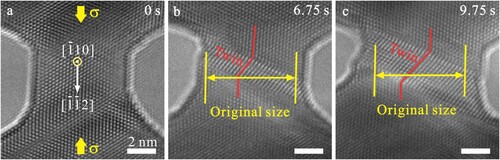
Not only the partial dislocation slip, but also full dislocation slip could activate surface atomic diffusion, causing thinning in Ag nanocrystal during compressive loading (Figure and Movie S4). As shown in Figure (a), a pristine 5.0-nm-diameter Ag nanocrystal was compressed along <112>-direction at room temperature under a strain rate of 10−3 s−1. Figure (a,b) show that one full dislocation slip caused the formation of two one-atomic-layer surface steps on both sides of the nanocrystal, increasing the nanocrystal width from 19 to 20 atomic layers. Given that 1/2[110] slip on the inclined (11) or (1
1) plane could not be observed along [
10]-direction, the slip event was further confirmed by quantitatively monitoring the change in gauge length between the two boundaries (white and yellow dashed lines) [Citation38,Citation39], as shown in Figure (a,b). The dislocation slip resulted in an abrupt length change of 0.17 nm (Figure (b)), in good agreement of the projection of a 1/2[110] slip on the [11
] loading direction. With further loading, the two as-formed surface steps migrated towards the ends of the nanocrystal continuously (Figure (c,d)), giving rise to a self-healing behavior as reported by Zhong et al. [Citation23] in the tensile test of Ag nanocrystals. The continuous flow of surface steps ultimately decreased the nanocrystal width by two atomic layers. Consequently, each full-dislocation-activated surface diffusion reduced the nanocrystal width by one atomic layer. The experimental observation of the continuous movement of the one-atomic-layer surface step upon compression was theoretically attributed to the stress- and curvature-driven surface atom diffusion (see Section 1 in Supplemental Material) [Citation21,Citation23,Citation39]. The atoms at the step edge sequentially hopped on {111} planes along <112> direction and diffused towards the ends of the nanocrystal to reduce the overall energy of the system, resulting in continuous surface ledge flow. The pathway for diffusional events at the SF sites, TBs and irregular surface nearby the preexisting dislocations should be akin to that for atom diffusion at the surface steps with a height of one atomic layer.
Figure 3. In situ TEM images showing full-dislocation-slip-induced surface atom diffusion. (a) A 5.0-nm-diameter Ag nanocrystal under [] compression at a strain rate of 10−3 s−1. (b) Formation of two surface steps (steps 1 and 2) formed by a full dislocation slip. (c–d) Surface-diffusion-assisted migration of atomic steps resulting in the reduction of the nanocrystal width. All scale bars are 2 nm.
![Figure 3. In situ TEM images showing full-dislocation-slip-induced surface atom diffusion. (a) A 5.0-nm-diameter Ag nanocrystal under [112¯] compression at a strain rate of 10−3 s−1. (b) Formation of two surface steps (steps 1 and 2) formed by a full dislocation slip. (c–d) Surface-diffusion-assisted migration of atomic steps resulting in the reduction of the nanocrystal width. All scale bars are 2 nm.](/cms/asset/a5c2993e-fc40-4d05-b557-1e0db9bc6c6e/tmrl_a_2108349_f0003_oc.jpg)
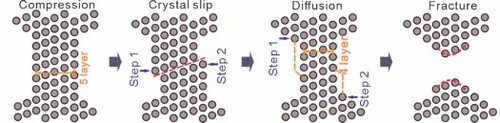
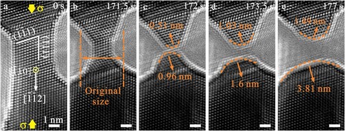
During the compression of the 4.3-nm-diameter Ag nanocrystal, a synergy of consecutively activated multiple thinning events discovered above gave rise to a continuous decrease in the nanocrystal width, as shown in Figure (a,b). With decreasing width, the chemical potential of surface atoms increased (see Eq. (S1) in Supplemental Material), driving surface mass transport more quickly [Citation23,Citation26]. As the diameter reduced to 1.71 nm (Figure (b)), curvature- and stress-driven surface atom diffusion led to the abnormal compression fracture of the Ag nanocrystal, which was akin to the failure process in the tensile test of Ag nanocrystals [Citation23]. Accompanied with the tensile-fracture-like failure, two tapered nanotips formed (Figure (c) and Movie S5). With the elapse of time, the curvature radii of the 0.51 and 0.96 nm-sized nanotips increased to 1.49 and 3.81 nm, respectively, and meanwhile the lengths of both nanotips decreased (Figure (c–e) and Movie S5), exhibiting a liquid-drop-like retraction behavior without dislocation activities and lattice structure change. The observed retraction behavior was attributed to surface atom bond breaking and atom transport along the free surface, which were driven by the high surface pressure of the fractured nanocrystal (see Section 2 in Supplemental Material) [Citation10].
Figure 4. Sequence of TEM images showing diffusion-induced compression fracture in a Ag nanocrystal. (a–b) Decrease in the nanocrystal width resulted from surface atom diffusion activated by preexisting dislocations and crystal slip. (c) Surface-diffusion-induced unusual compression fracture of the nanocrystal, forming two tapered nanotips. (d–e) Liquid-drop-like retraction behavior in the fracture nanocrystal. All scale bars are 1 nm.
Recently, Zhong et al. [Citation23] reported that the diffusion stability limits for Ag nanocrystal was estimated to be 15 nm, above which diffusional events at free surface were quite limited. To confirm the universality of the abnormal thinning and compression fracture observed in the sub-15-nm-sized Ag nanocrystals during compression, a 16.2-nm-diameter Ag nanocrystal was tested along <112>-direction at room temperature under a strain rate of 10−3 s−1. During compression, slip-activated surface atom diffusion gave rise to consecutive thinning events, leading to the continuous decrease in the nanocrystal's width (Figure S2 and S3(a-d)). When the diameter of the Ag nanocrystal decreased to 2.65 nm, surface diffusional events ultimately led to the tensile-fracture-like failure of the nanocrystal (Figure S3(d)). Subsequently, liquid-drop-like retraction behavior, driven by surface pressure, occurred in the fractured nanocrystal (Figure S3(e-h)). Moreover, in all the Ag nanocrystals with an aspect ratio ranging from 0.68 to 2.1 and tested by in situ TEM under the strain rate of 10−3 s−1, surface-diffusion-mediated unusual thinning and compression fracture occurred (Figure S4).
To further probe the compressive deformation behavior of Ag nanocrystals, in situ compression test of a pristine 6.1-nm-diameter Ag nanocrystal at room temperature under a high stain rate of 0.06 s−1 was performed along <112>-direction (Figure ). Different from the abnormal thinning and compression fracture observed at a low strain rate of 10−3 s−1, consecutive thickening, mediated by dislocation slip, occurred in the Ag nanocrystal at a high strain rate, which was attributed to the strain-rate sensitive nature of diffusional mechanisms [Citation16,Citation23,Citation39]. Quite limited surface atom diffusion occurred at a high strain rate, incapable of eliminating the surface steps formed by dislocation slip. Consequently, dislocation activities continuously generated nearly immobile surface steps, resulting in thickening upon compression. Hence, the occurrence of unusual thinning and fracture during Ag nanocrystal compression, resulting from coupled displacive-diffusive deformation, required that the crystal thinning rate arising from surface atom diffusion be larger than the thickening rate from crystal slip. In addition to the applied strain rate, the sample dimensions (diameter, length and aspect ratio) and the type of materials (surface mobility and surface energy) affect the competition between the thickening by crystal slip and thinning by surface diffusion in metallic nanocrystal during compression (see Section 3 in Supplemental Material) [Citation10,Citation16,Citation21,Citation23]. For a Ag nanocrystal with given aspect ratio and dimensions tested at room temperature, there is a critical strain rate below and above which thinning and thickening, mediated by coupled displacive-diffusive mechanism, could occur in the nanocrystal, respectively.
Figure 5. Compression-induced thickening in a Ag nanocrystal at a high strain rate of 0.06 s−1. (a) TEM image of a pristine 6.1-nm-diameter Ag nanocrystal under <112> compression loading at room temperature. (b–c) Sequential TEM images showing consecutive thickening in Ag nanocrystal mediated by deformation twinning. All scale bars are 2 nm.
4. Discussion
Different from the prior study that dislocation-free diffusional deformation mediated liquid-like thickening during the compression of a sub-10-nm Ag nanoparticle [Citation21], our work revealed that coupled displacive-diffusive deformation induced unusual thinning and tensile-fracture-like failure during Ag nanocrystal compression, which may be attributed to the different sample shapes and experimental conditions. Given that the surface-to-volume ratio of nanostructured metals was size- and shape- dependent, surface atom diffusion in nanoparticle was stronger than that in nanocrystal with same feature size [Citation8,Citation40,Citation41]. Furthermore, the compression testing of Ag nanoparticle was conducted through the movement of Ag-nanoparticle-decorated W tip toward ZrO2 surface, during which Ag-W and Ag-ZrO2 interfaces could act as a highway for diffusional events upon loading (Figure S5). Coble-like diffusional processes at heterogeneous interfaces and free surfaces were sufficient to accommodate the applied strain on the nanoparticle, causing continuous mass transport along interfaces and surfaces (Figure S5) and the consequent liquid-like-thickening. In contrast, no GBs or heterogeneous interfaces existed between the Ag nanocrystal and substrate using in situ nanowelding (see Methods section). Given that the contribution of bulk diffusion to strain was quite limited at room temperature [Citation26], additional displacive mechanisms should be activated in nanocrystal to accommodate deformation, generating atomic-scale steps at free surfaces (Figure S6(a)). Due to curvature- and stress-driven diffusional flow of surface atoms at step edge, surface step with high chemical potential migrated towards the ends of the nanocrystal with low chemical potential, causing thinning and ultimate compression fracture in Ag nanocrystals (Figure S6(b) and Section 1 in Supplemental Material).
Our findings indicated that surface atom diffusion played a critical role in the compression-induced abnormal thinning and fracture in Ag nanocrystals, in contrast to the recent observations in FCC and body-centered-cubic (BCC) sub-micro pillars fabricated by focus ion beam (FIB) cutting, in which thickening behavior, resulting from pure dislocation plasticity, were observed during compression [Citation13,Citation42–47]. Such difference in compressive deformation behavior between metallic nanocrystals and sub-micro pillars may come from the following reasons: (1) The sample diameters of the nanocrystals adopted in this work (4.3, 5.0 and 16.2 nm) were much smaller than those for submicron-sized pillars. Given that the competition between displacive and diffusive deformations is size-dependent [Citation16–18], weak or even no surface atom diffusion may occur in submicron pillars. (2) Compared to Au, W, molybdenum (Mo), tantalum (Ta), niobium (Nb) and nickel (Ni) sub-micro pillars in the previous studies [Citation13,Citation42–47], the melting point for Ag nanocrystal is lower. Surface atom diffusion, depending on the ratio of experimental temperature and melting point of materials [Citation10,Citation16], was stronger in low-melting-point metals tested at room temperature, compared to the high-melting-point ones. In addition, with the reduction in sample size, the melting point decreases and diffusion coefficient and increases, respectively [Citation48]. Hence, surface atom diffusion could be observed in the Ag nanocrystals rather than other various metallic sub-micro pillars. (3) In situ nanowelding was employed in this study to fabricate Ag nanocrystals with clean surfaces, which were ideal for studying diffusive plasticity at free surface [Citation23,Citation49]. By contrast, surface oxidation/contamination layer, introduced by FIB cutting, probably suppressed mass transport along free surfaces in submicron pillar in the previous studies [Citation8]. To the best of our knowledge, the consecutively occurring thinning and the ultimate tensile-fracture-like failure during Ag nanocrystal compression in this study have never been reported before, due to technical difficulties in fabricating nanoscale metals with clean surfaces. Together with the previous studies [Citation42–47], our study provides a comprehensive understanding of the atomic-scale compressive deformation behavior in small-sized metals, and new clues to design reliable nanoscale-metal-based devices.
5. Conclusion
In conclusion, in situ HRTEM compression experiments have revealed that preexisting dislocation and crystal slip served as stimuli to activate surface atom diffusion, resulting in abnormal thinning in Ag nanocrystals during compression. As the width of Ag nanocrystal decreased to a critical value, unusual tensile-fracture-like failure occurred, which was resulted from the diffusion of surface atoms. Our findings not only advance the current understanding of compressive deformation behavior in metallic nanocrystals, but also shed light on atomic-scale coupled diffusive–displacive deformation mechanisms, providing new clues to design mechanically reliable nanoscale metals for electrical devices.
Supplemental Material
Download Zip (34.9 MB)Disclosure statement
No potential conflict of interest was reported by the author(s).
Additional information
Funding
References
- Loh OY, Espinosa HD. Nanoelectromechanical contact switches. Nat Nanotechnol. 2012;7(5):283–295.
- Gao W, Emaminejad S, Nyein HYY, et al. Fully integrated wearable sensor arrays for multiplexed in situ perspiration analysis. Nature. 2016;529(7587):509–514.
- Gong S, Schwalb W, Wang Y, et al. A wearable and highly sensitive pressure sensor with ultrathin gold nanowires. Nat Commun. 2014;5(1):1–8.
- Cui Z, Han Y, Huang Q, et al. Electrohydrodynamic printing of silver nanowires for flexible and stretchable electronics. Nanoscale. 2018;10(15):6806–6811.
- Liang J, Li L, Tong K, et al. Silver nanowire percolation network soldered with graphene oxide at room temperature and its application for fully stretchable polymer light-emitting diodes. ACS Nano. 2014;8(2):1590–1600.
- Xu F, Zhu Y. Highly conductive and stretchable silver nanowire conductors. Adv Mater. 2012;24(37):5117–5122.
- Yin S, Cheng G, Zhu Y, et al. Competition between shear localization and tensile detwinning in twinned nanowires. Phys Rev Mater. 2020;4(2):023603.
- Zheng S, Mao SX. Advances in experimental mechanics at atomic scale. Extreme Mech Lett. 2021;45:101284.
- Wang J, Wang Y, Cai W, et al. Discrete shear band plasticity through dislocation activities in body-centered cubic tungsten nanowires. Sci Rep. 2018 Mar 15;8:1–8.
- Kong D, Xin T, Sun S, et al. Surface energy driven liquid-drop-like pseudoelastic behaviors and in situ atomistic mechanisms of small-sized face-centered-cubic metals. Nano Lett. 2019;19(1):292–298.
- Ramachandramoorthy R, Wang Y, Aghaei A, et al. Reliability of single crystal silver nanowire-based systems: stress assisted instabilities. ACS Nano. 2017;11(5):4768–4776.
- Li Q-J, Xu B, Hara S, et al. Sample-size-dependent surface dislocation nucleation in nanoscale crystals. Acta Mater. 2018;145:19–29.
- Shan ZW, Mishra RK, Syed Asif SA, et al. Mechanical annealing and source-limited deformation in submicrometre-diameter Ni crystals. Nat Mater. 2008;7(2):115–119.
- Chen LY, He M-R, Shin J, et al. Measuring surface dislocation nucleation in defect-scarce nanostructures. Nat Mater. 2015;14(7):707–713.
- Weinberger CR, Cai W. Plasticity of metal nanowires. J Mater Chem. 2012;22(8):3277–3292.
- Tian L, Li J, Sun J, et al. Visualizing size-dependent deformation mechanism transition in Sn. Sci Rep. 2013;3(1):2113.
- Guo W, Wang Z, Li J. Diffusive versus displacive contact plasticity of nanoscale asperities: temperature- and velocity-dependent strongest size. Nano Lett. 2015;15(10):6582–6585.
- Zhu T, Li J. Ultra-strength materials. Prog Mater Sci. 2010;55(7):710–757.
- Li QJ, Ma E. When ‘smaller is stronger’ no longer holds. Mater Res Lett. 2018;6(5):283–292.
- Xie D-G, Nie Z-Y, Shinzato S, et al. Controlled growth of single-crystalline metal nanowires via thermomigration across a nanoscale junction. Nat Commun. 2019;10(1):1–8.
- Sun J, He L, Lo Y-C, et al. Liquid-like pseudoelasticity of sub-10-nm crystalline silver particles. Nat Mater. 2014;13(11):1007–1012.
- Strachan DR, Smith DE, Fischbein MD, et al. Clean electromigrated nanogaps imaged by transmission electron microscopy. Nano Lett. 2006;6(3):441–444.
- Zhong L, Sansoz F, He Y, et al. Slip-activated surface creep with room-temperature super-elongation in metallic nanocrystals. Nat Mater. 2017;16(4):439–445.
- Wang B, Han Y, Xu S, et al. Mechanically assisted self-healing of ultrathin gold nanowires. Small. 2018;14(20):1704085.
- Rodrigues V, Fuhrer T, Ugarte D. Signature of atomic structure in the quantum conductance of gold nanowires. Phys Rev Lett. 2000;85(19):4124–4127.
- Sun S, Kong D, Li D, et al. Atomistic mechanism of stress-induced combined slip and diffusion in Sub-5 nanometer-sized Ag nanowires. ACS Nano. 2019;13(8):8708–8716.
- Xie KY, Shrestha S, Cao Y, et al. The effect of pre-existing defects on the strength and deformation behavior of α-Fe nanopillars. Acta Mater. 2013;61(2):439–452.
- Wang J, Zeng Z, Weinberger CR, et al. In situ atomic-scale observation of twinning-dominated deformation in nanoscale body-centred cubic tungsten. Nat Mater. 2015;14(6):594–600.
- Li P, Han Y, Zhou X, et al. Thermal effect and Rayleigh instability of ultrathin 4H hexagonal gold nanoribbons. Matter. 2020;2(3):658–665.
- Egerton RF, Wang F, Crozier PA. Beam-induced damage to thin specimens in an intense electron probe. Microsc Microanal. 2006;12(1):65–71.
- Kim SY, Lee I-H, Jun S. Transition-pathway models of atomic diffusion on fcc metal surfaces. I. Flat surfaces. Phys Rev B. 2007;76(24):245407.
- Hummel R, Geier H. Activation energy for electrotransport in thin silver and gold films. Thin Solid Films. 1975;25(2):335–342.
- Ala-Nissila T, Ferrando R, Ying S. Collective and single particle diffusion on surfaces. Adv Phys. 2002;51(3):949–1078.
- Egerton R, Li P, Malac M. Radiation damage in the TEM and SEM. Micron. 2004;35(6):399–409.
- Takahashi Y, Suzuki A, Furutaku S, et al. Bragg x-ray ptychography of a silicon crystal: visualization of the dislocation strain field and the production of a vortex beam. Phys Rev B. 2013;87(12):121201.
- Anderson PM, Hirth JP, Lothe J. Theory of dislocations. 3rd ed. New York: Cambridge University Press; 2017. English.
- Wang B, Liu M, Wang Y, et al. Structures and energetics of silver and gold nanoparticles. J Phys Chem C. 2011;115(23):11374–11381.
- Zheng S, Shinzato S, Ogata S, et al. Experimental molecular dynamics for individual atomic-scale plastic events in nanoscale crystals. J Mech Phys Solids. 2021;158:104687.
- Wang X, Zheng S, Shinzato S, et al. Atomistic processes of surface-diffusion-induced abnormal softening in nanoscale metallic crystals. Nat Commun. 2021;12(1):1–9.
- Mishra S, Gupta SK, Jha PK, et al. Study of dimension dependent diffusion coefficient of titanium dioxide nanoparticles. Mater Chem Phys. 2010;123(2-3):791–794.
- Guisbiers G, Kazan M, Van Overschelde O, et al. Mechanical and thermal properties of metallic and semiconductive nanostructures. J Phys Chem C. 2008;112(11):4097–4103.
- Greer JR, Weinberger CR, Cai W. Comparing the strength of fcc and bcc sub-micrometer pillars: compression experiments and dislocation dynamics simulations. Mater Sci Eng A. 2008;493(1-2):21–25.
- Brinckmann S, Kim J-Y, Greer JR. Fundamental differences in mechanical behavior between two types of crystals at the nanoscale. Phys Rev Lett. 2008;100(15):155502.
- Kim J-Y, Jong DC, Greer JR. Tensile and compressive behavior of tungsten, molybdenum, tantalum and niobium at the nanoscale. Acta Mater. 2010;58(7):2355–2363.
- Huang L, Li Q-J, Shan Z-W, et al. A new regime for mechanical annealing and strong sample-size strengthening in body centred cubic molybdenum. Nat Commun. 2011;2(1):1–6.
- Schneider AS, Kaufmann D, Clark BG, et al. Correlation between critical temperature and strength of small-scale bcc pillars. Phys Rev Lett. 2009;103(10):105501.
- Uchic MD, Dimiduk DM, Florando JN, et al. Sample dimensions influence strength and crystal plasticity. Science. 2004;305(5686):986–989.
- Dick K, Dhanasekaran T, Zhang Z, et al. Size-dependent melting of silica-encapsulated gold nanoparticles. J Am Chem Soc. 2002;124(10):2312–2317.
- Cao G, Wang J, Du K, et al. Superplasticity in gold nanowires through the operation of multiple slip systems. Adv Funct Mater. 2018;28(51):1805258.