
 ?Mathematical formulae have been encoded as MathML and are displayed in this HTML version using MathJax in order to improve their display. Uncheck the box to turn MathJax off. This feature requires Javascript. Click on a formula to zoom.
Abstract
The performance and potential of energy-harvesting devices depend strongly on the performance and specific properties of materials and used technology. The recent explosion in capability of embedded electronics has not been matched by battery technology. The slow growth of battery energy density has limited device lifetime and added volume and weight. The amount of energy from harvesting is typically small and variable, requiring circuits and architectures which are low power and can scale their power consumption with user requirements and available energy. The energy harvesting research falls into two key areas. One is developing optimal structures of energy harvesting and the other is designing electronic circuits that are efficient enough to store the generated charge. Optimization of microelectronic devices to reduce energy consumption, while all devices strive to achieve good efficiency, balancing performance and power consumption, the application area will dictate design constraints such as size, energy budget, and maximum power. Regarding the research area of optimal design of electronic circuits, a highly efficient CMOS rectifier for vibrational energy harvesting system is proposed. Based on the design considerations, rectifier plays an important role in the application of energy harvesting system and wireless power transfer system. So, the performance of the rectifier decides the efficiency of the system. The proposed low voltage Rectifier is designed for operating frequency of 13.56 MHz using two-stage structure and an Improved precision active diode under a standard 0.18um CMOS process can perform the minimum operating voltage is lower than previous published paper and the rectifier can work at a wide range of input voltage amplitudes of 0.45 V up to 1.95 V. So, the proposed rectifier is suitable to work in Different Types of vibrational energy harvesting system, Electrostatic Energy harvester, Electromagnetic Energy Harvester, Piezoelectric Energy Harvester. The proposed rectifier can achieve peak voltage conversion efficiency of over 81% and power efficiency over 79%. Simulated power consumption of the rectifier is 0.23uW, which is about 28% smaller than the best recently published results.
Keywords:
- Embedded electronics
- energy harvesting
- CMOS circuits
- battery-less technology
- mechanical vibration
- wearable and embedded sensors
- low power circuits and architectures
- ICT information communication technology
- energy efficiency
- energy sustainability
- low power embedded systems
- improved precision active diode
- low voltage rectifier
PUBLIC INTEREST STATEMENT
Energy harvesting, the collection of small amounts of ambient energy to power wireless devices, is very promising technology for applications where batteries are impractical, such as body sensor networks and inaccessible remote systems. The desire to use self-powered devices With few limitations such as low amount of power generated using the energy harvesters is the goal of researchers who working towards generating new methods. These methods would help in placing the energy harvesters as one of the best sources to power portable devices in the field of wireless technology. Embedded Systems (ES) are regarded as an innovative and light weight technical solutions. Main benefits of embedded systems are connectivity, productive performance and cheap cost of component. These advantages make embedded systems widely applicable in the industry of implantable and wearable devices. The energy harvesting research falls into two key areas. One is developing optimal structures of energy harvesting and the other is designing electronic circuits that are efficient enough to store the generated charge.
1. Introduction
The field of energy harvesting and wireless power transfer are very hot research topics recently and affected by the advances of many different researches. Energy harvesting, the collection of small amounts of ambient energy to power wireless devices, is very promising technology for applications where batteries are impractical, such as body sensor networks and inaccessible remote systems. Energy Harvesting (EH) can be defined as a process wherein the sources such as mechanical load, vibrations, temperature gradients and light, etc., are scavenged and converted to obtain relatively small levels of power in the nW-mW range (Gilbert & Balouchi, Citation2018; Raghunathan et al., Citation2015; Sun et al., Citation2012). Figure shows the general types of portable energy systems (Ottman et al., Citation2012). Harvesting energy from the environment is being considered as a viable option to replace the current power supplies for energy-constrained embedded systems. The desire to use self-powered devices drives to achieve enormous growth in the field of energy harvesting. With the few limitations such as low amount of power generated using the power harvesters, the researchers are working towards generating new methods. These methods would help in placing the energy harvesters as one of the best sources to power portable devices in the field of wireless technology. Embedded Systems (ES) are regarded as an innovative and light weight technical solutions (Sun et al., Citation2012). Main benefits of embedded systems are connectivity, productive performance and cheap cost of components (Gilbert & Balouchi, Citation2018). These advantages make embedded systems widely applicable in the industry of implantable and wearable devices. As the framework of Nano-medicine has taken advantage of computing devices integration. A variety of electronic medical tools are being employed to address the needs of healthcare system (Raghunathan et al., Citation2015). For example, continuous and automatic management of health conditions would not be possible without involvement of implantable medical devices (IMDs) which are type of medical devices embedded inside the human body for medical intervention. Although implantable devices so far have met wide approval of the professionals, several limitations in the design and structure of IMDs still impede further expansion of the implant market. Hence, the development of completely new technique is strongly required to prevent any undesired external impact on IMDs.
Figure 1. General types of portable energy systems (Ottman et al., Citation2012).
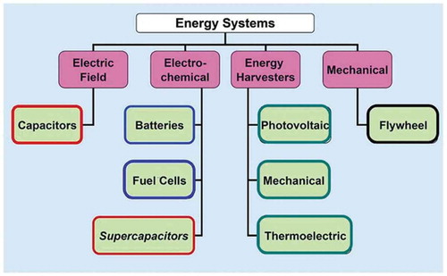
Figure 2. Methods and processes involved in ambient energy harvesting system (Yildiz, Citation2007).
1.1. Energy and power issues for embedded systems
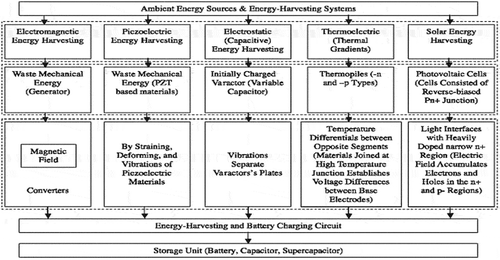
The energy and power issue for Embedded systems is the “capability of performing work.” Power, being equal to the work divided by the time that it takes to do it, indicates how fast this work is done for a certain amount of energy or how much energy is consumed to achieve a task, e.g., a computational operation (in a specified time interval). The power required to operate current Embedded systems ranges from the mW level for small autonomous sensor systems to tens of MWs for HPC systems. In between these power levels lie a large number of devices including embedded sensors, mobile phones, smartphones, tablets, personal computers, servers, and cloud computing storage systems. The use of Embedded systems has been driven by the continuous scaling of silicon chips. The original drivers for scaling came from improving the performance of computers, but as the size of transistors was reduced, so was the power consumption enabling many portable systems to be developed. Figure shows Methods and processes involved in ambient energy harvesting system (Sauer et al., Citation2015; Li & Bashirullah, Citation2017)
1.2. Chip level (key device challenges)
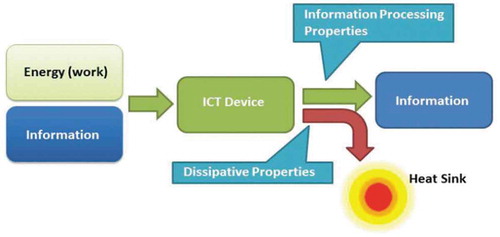
A generic ICT device can be viewed as a machine that processes information while transforming work into heat and heat into work. Pioneering research developed in the last century has shown that information processing is intimately related to energy management(Cevik et al., Citation2015; Yen & Lang, Citation2006). An ICT device shown in Figure is a machine that inputs information and energy (under the form of work), processes both and outputs information and energy (under the form of heat). From this perspective energy dissipation via heat production and energy transformation processes are two aspects of the same topic: energy management at the micro- and nanoscales. For our purposes, energy efficiency is defined as the percentage of energy input to a device consumed in useful work and not wasted as heat. This definition, however, may not apply when we have to deal with processes taking place at the nanoscale.
Figure 3. An ICT device is a machine that inputs information and energy (form of work) and processes both and outputs information and energy (form of heat).
1.3. CMOS device challenges can be summarized as
The cost of the lowest energy devices requires the latest CMOS technology node that now requires enormous economies of scale due to the cost of the foundries and technology.
The scaling of transistors to smaller dimensions is now not expected to decrease the switching energy significantly.
If there is a change of the basic switching device (CMOS) to move to a significantly lower energy technology, then circuit architectures, design tools, verification, operating systems, and software may require rewriting or complete changes for basic operation or optimal performance.
Driving interconnects with multiple fan-out or an antenna have fundamental energy and noise limits that makes ultra-low energy consumption difficult.
Devices with learning capability, that learn logic configurations and devices that learn by example.
Integration of RF devices and components.
Optical devices, e.g., Si photonics for communications and optical sensing modalities.
Micro Electro Mechanical Systems (MEMS) and Nano Electro Mechanical Systems (NEMS).
Integration of sensors.
Significant opportunities can be divided into continued scaling of conventional transistor devices (termed More Moore) and adding new device concepts for computation (termed beyond Moore or beyond CMOS) or new functionality onto the base CMOS technology (termed More than Moore). The key concept in More Moore is the circuit architectures will be similar to present CMOS architectures and only the devices, voltages, or currents are changed. More Moore is looking at the challenges of scaling CMOS devices to dimensions below 10 nm (Guo & Lee, Citation2009).
1.4. Circuits level (micro-architecture level)
The micro-architecture level considers the integration of many of the underlying fundamental device technologies. Transistor technologies and silicon processes are combined into useful blocks such as memory, control, and arithmetic that together form computational device, often a processor or an accelerator. The scope for that integrated device is very broad, including ultralow power embedded devices, through general-purpose processors, up to high-performance network-on-chip components. Current manufacturing of semiconductor devices has hit a fundamental efficiency limit called the “energy wall” that prevents reduction of energy consumption when transistor size scales down for forthcoming technology nodes. Both at small-scale Embedded Systems and at a large-scale HPC/Data centers (Din et al., Citation2014; Lu et al., Citation2011). The ultimate limits from architecture designs are almost impossible to drive, but based on current technology, there is general agreement by academia and industry that new architectures are more promising to significantly reduce power consumption than improving the energy consumption of the basic switching device in the circuit. The amount of energy consumption from a circuit architecture design for a given CMOS technology node is heavily dependent on how specific (i.e., optimized for a single or few tasks) or how general (i.e., undertake many different computations) a design has to deliver. Applications Specific Integrated Circuits (ASICs) designed for a single task can be optimized proving the lowest energy consumption, but such designs have no flexibility and cannot be reprogrammed. For microprocessors or microcontrollers that must be able to undertake a wide range of tasks, optimization to reduce energy consumption is significantly more difficult. Micro-architecture exploits what is physically possible with contemporary technology and presents an interface through which other hardware and software can use the device. In hardware terms, this interface is, of course, physical and will typically obey a specified protocol. In software terms, the processing device presents a set of possible operations through an Instruction Set Architecture (ISA). If the ISA is a description of the behaviors of the device, then the microarchitecture is the implementation of those behaviors. Advances in physics, transistor design, and device manufacturing techniques can benefit microelectronic devices of all kinds; however, microarchitecture design decisions are heavily influenced by the target market of the resultant product. While all devices strive to achieve good efficiency, balancing performance and power consumption, the application area will dictate design constraints such as size, the energy budget, and maximum power. We may group micro-architecture characteristics grouped into four areas: deeply embedded, embedded/mobile, general purpose, and servers/high-performance. These are not necessarily strict boundaries and properties often transfer between areas over time, as technology or commercial pressures permit. At present, micro-architectures have significantly different drivers for HPC/data centers, general purpose, and embedded systems/portable systems.
1.5. Deeply embedded (smart cards)
An example of a deeply embedded device is the processor in a smart card. It must fit within a credit card form factor, cannot be modified once sent to the customer, be powered by a battery-backed device, and obey strict security protocols. A new generation of deeply embedded devices is smart autonomous sensors, which due to their ability to seamlessly integrate with the environment have given rise to cyber-physical systems (CPS) and IoT platforms. This requires integration of heterogeneous components dedicated to signal acquisition (e.g., analogue-to-digital converters (ADCs)), processing (digital signal processors), and environment manipulation (actuators). The embedded system may also typically include wireless communication and run on batteries together with energy harvesters. Hence, one or more of the following constraints may apply: • Physical size must be small, from millimetres to a few centimetres, depending on application. • The energy budget is finite as power may be intermittent or limited, often sub-watt or sub-milliwatt. • Operating temperatures may vary significantly and the removal of excess heat quickly may not be possible. • Reliability is essential, because servicing may be difficult, expensive, or impossible. • Predictable behavior may be required to guarantee safety criteria or always-correct device functionality. All of the above points are relevant in an energy context. The energy consumption of the device dictates the temperature it runs at, the type of cooling required, how much processing and communication can be performed, and how long it will live. Predictable energy consumption is required to guarantee a particular battery life. To meet design goals within a small energy budget envelope, the design of each of the components is highly tailored to the targeted application (Do et al., Citation2013; Lu et al., Citation2017). Circuit designs include low-voltage, power-efficient ADCs and filters, instrumentation amplifiers, domain-specific memory organizations, and schemes for energy/power management and transfer.
The micro-architectures of deeply embedded systems take various forms, but the following traits are common: • They provide predictable execution times for many or all of the ISA instructions they support. • Their functional blocks, such as arithmetic and memory units, are often simpler than larger counterparts, to reduce power, improve predictability, and keep the device small. • Their memory hierarchy is flat, avoiding caches that would impact predictability and increase device complexity. • Programs may execute directly out of integrated flash storage, with RAM only used for read-write data.
1.6. Embedded/mobile devices
The line between embedded and deeply embedded is often blurry, but for the present purpose, we group regular embedded devices with mobile devices, in order to set the grouping in terms of energy requirements. Such devices may still have real-time constraints, small size requirements, and sub-watt power envelopes. An example of an embedded device is the controller chip on a hard disk or a solid-state disk. They cannot be replaced, so their failure effectively renders the entire disk useless. The software running on them is difficult or undesirable to update in the interests of data security. They interact with components that have strict timing protocols, and missed deadlines will potentially result in data loss or corruption. They must fit within the form-factor of the device, e.g., the whole device may be as small as 12 × 16 mm (the smallest of the possible M.2 format of expansion devices used in laptops at the time of writing). However, the performance requirement and available power are higher than deeply embedded devices, hence, this may be considered embedded rather than deeply embedded. Mobile and embedded systems typically have the following microarchitecture properties: • Heavily integrated into system-on-chip (SoC), providing various peripherals and multicore computational capabilities in a single chip. • Larger storage and memory capacity than deeply embedded, in the order of gigabytes in current devices. • Cache hierarchies for better memory performance. • Sub-watt power constraints. • Must fit within relatively small form factors, such as a mobile phone. • More complex application sets and usage patterns.
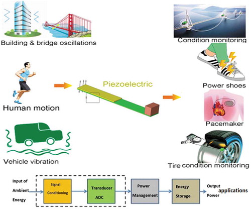
2. Various sources of energy harvesting for embedded systems
The energy harvesting sources can be used to increase the lifetime and capability of the devices by either replacing the battery usage (Cevik et al., Citation2015; Do et al., Citation2013; Kamarudin et al., Citation2007; Kwon & Rincón-Mora, Citation2014). The devices powered by energy harvesters can be used to provide vital information on operational and structural circumstances by placing them in inaccessible locations (Cook et al., Citation2006). There is an increasingly carried out research on energy harvesting (Gilbert & Balouchi, Citation2018; Li & Bashirullah, Citation2017; Ottman et al., Citation2012; Raghunathan et al., Citation2015; Sauer et al., Citation2015; Sun et al., Citation2012; Yildiz, Citation2007). This part is a survey of various sources available for energy harvesting. The various sources for energy harvesting are wind turbines, photovoltaic cells, thermoelectric generators and mechanical vibration devices such as piezoelectric devices, electromagnetic devices (Cook et al., Citation2006). Table shows some of the harvesting methods with their power generation capability (Sauer et al., Citation2015). Figure ) Types of ambient energy sources suitable for energy harvesting. The general properties to be considered to characterize a portable energy supplier are electrical properties such as power density, maximum voltage and current; physical properties such as size, shape and weight; environmental properties such as water resistance and operating temperature range; as well as operational properties. Special concern should be taken while using the energy harvesters in embedded systems to improve the performance and lifetime of the system (Mitcheson et al., Citation2008).
Figure 4. General block diagram of energy harvesting system.
Figure 5. Types of ambient energy sources.
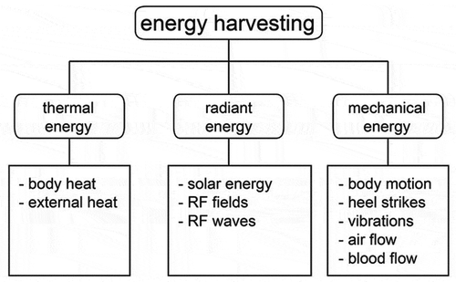
Table 1. Energy harvesting sources (Sauer et al., Citation2015)
2.1. Mechanical vibration energy harvesting
When a device is subjected to vibration, an inertial mass can be used to create movement. This movement can be converted to electrical energy using three mechanisms: piezoelectric, electrostatic, and electromagnetic. The form of energy utilized here is the mechanical energy.
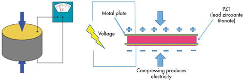
2.1.1. Piezoelectric materials
The piezoelectric materials convert mechanical energy from pressure, vibrations or force into electricity. They are capable of generating electrical charge when a mechanical load is applied on them. This property of piezoelectric materials is considered by the researchers to develop various piezoelectric harvesters in order to power different applications. Due to their inherent ability to detect vibrations, piezoelectric materials have become a viable energy scavenging source. Currently a wide variety of piezoelectric materials are available and the appropriate choice for sensing, actuating, or harvesting energy depends on their characteristics. Some are naturally occurring materials such as quartz. Polycrystalline ceramic is a common piezoelectric material. Lead Zirconate Titanate (PZT) is being considered since it shows a high efficiency of mechanical to electrical energy conversion (Mitcheson et al., Citation2004). With their anisotropic characteristics, the properties of the piezoelectric material differ depending upon the direction of forces and orientation of the polarization and electrodes (Cevik et al., Citation2015; Guo & Lee, Citation2009; Kamarudin et al., Citation2007; Lu et al., Citation2017; Torfs et al., Citation2006).
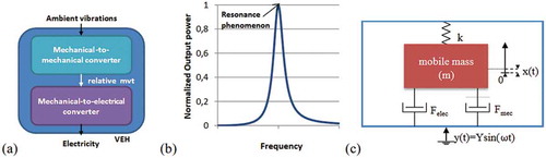
Figure 6. Vibration Energy Harvesters: (a) concept (b) resonance phenomenon and (c) mode (Torfs et al., Citation2006).
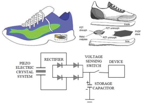
Using piezoelectric materials to harvest energy requires a mode of storing the energy generated. This means they can either implement a circuit used to store the energy harvested or a circuit developed to utilize the energy harvested in producing excess energy. The energy harvested can be stored in rechargeable batteries instead of using capacitors to store the energy (Cook et al., Citation2006; Kamarudin et al., Citation2007; Torfs et al., Citation2006). The attribute of common capacitors to discharge quickly makes them unsuitable as energy storage devices in computational electronics. Umeda, et al. [36] used a piezo-generator made of a bridge rectifier~ and a capacitor to store the energy as in Figure . This resulted in achieving a maximum efficiency of 35% that is three times that of the energy harvested from a solar cell (Pop et al., Citation2007).
Figure 7. Piezoelectric materials.
A self-powered mechanical strain energy sensor designed by Elvin, et al. (Kamarudin et al., Citation2007) illustrates a simple beam bending experiment conducted to produce electrical energy from the mechanical stress applied. Here a piezo film sensor attached to a beam is used to generate the electrical signal. According to Glynne-Jones, et al. (Torfs et al., Citation2006), an energy harvesting device is being developed where a thick film of piezoelectric layer is deposited on to a thin steel beam. When the beam is resonated, the piezoelectric material is deformed and electrical energy is generated. By changing the material used, the magnitude of power generated can be improved. The earliest example for extracting electrical energy from piezoelectric material is from the impact of dropping a steel ball bearing onto a piezoelectric transducer. This energy was then stored in a capacitor or a battery (Cevik et al., Citation2015; Mitcheson et al., Citation2004; Renaud et al., Citation2007). For example, a piezoelectric material such as polyvinylidene fluoride (PVDF) is attached to the heel of a shoe (Din et al., Citation2014; Yen & Lang, Citation2006). When the shoe strikes the ground, the energy released is converted by the piezoelectric material into electric charge. This charge can be used for some high-end sneaker designs (Renaud et al., Citation2005; Sterken et al., Citation2004, Citation2007).
Figure 8. Mechanical vibration energy harvesting, excitations, energy harvester, and its applications.
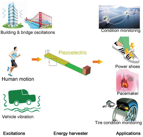
Figure 9. A self-powered mechanical strain energy sensor (Kamarudin et al., Citation2007).
The piezoelectric energy harvesting research falls into two key areas. One is developing optimal energy harvesting structures and the other is designing electrical circuits that are efficient enough to store the generated charge. The research carried out at The University of Pittsburgh focuses on the first area, where the goal is to create small, lightweight structures that couple efficiently to mechanical excitation and produce usable electrical energy. This team is concentrating on developing optimal devices which are capable of converting the ambient mechanical energy available into electrical energy. Recently, a new power-conditioning circuit for piezoelectric energy scavenging systems has been proposed. Ottman, et al. (Sterken et al., Citation2003; Martinez et al., Citation2018) offers a greatly improved efficiency over existing designs under sinusoidal vibration (Siddiqui et al., Citation2018).
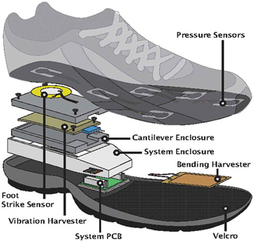
Figure 10. Expanded view of Shoe system and all integrated components.
This circuit uses a step-down converter and harvested more than four times the power of the same circuit when the converter was not used. More than 70 mW of power was harvested from the new system, which is sufficient to power a wireless sensor network node, even in continuous receive mode. Later a simplified converter was employed which helped in producing more power. This work can be considered as a prominent step in the usage of energy generated from using piezoelectric materials. The properties of piezoelectric materials vary with age, stress and temperature. The possible advantages of using piezoelectric materials are the direct generation of desired voltage since they do not need a separate voltage source and additional components. These generators are compatible with the MEMs. These generators are the simplest and can be used in force and impact-coupled harvesting applications (Jin et al., Citation2018; Zhao et al., Citation2018). Some disadvantages are that piezoelectric materials are brittle in nature and sometimes allow the leakage of charge (Anton & Sodano, Citation2007).
2.1.2. Electromagnetic energy harvesting
Electromagnetic Energy Harvesting can be achieved by the principle of electromagnetic induction. Electromagnetic induction is defined as the process of generating voltage in a conductor by changing the magnetic field around the conductor. One of the most effective ways of producing electromagnetic induction for energy harvesting is with the help of permanent magnets, a coil and a resonating cantilever beam (Cevik et al., Citation2015). El-Hami, et al. describe a vibration-based electromechanical power generator that consisted of a cantilever beam and a pair of magnets. Since the late 1990 s, various researchers (Martinez et al., Citation2018; Peters et al., Citation2011; Qiang et al., Citation2010; Shenck & Paradiso, Citation2001; Sterken et al., Citation2003) have identified the techniques employed to generate power from electromagnetic resources. The electromagnetic generators designed have the advantage of being enclosed and can be protected from the outside environment. Electromagnetic induction provides the advantage of improved reliability and reduced mechanical damping as there would not be any mechanical contact between any parts; also, no separate voltage source is required. However, electromagnetic materials are bulky in size and are complicated to integrate with MEMs. Bayrashev, et al. and Staley, et al. concentrated on harvesting energy from magnetostrictive materials (Li & Bashirullah, Citation2017). These magnetostrictive materials are used to build actuators and sensors as they have the capability of converting magnetic energy into kinetic energy. These materials are highly flexible, are suited to high frequency vibration and overcome the limitations of the other vibrational sources. To harvest energy by using magnetostrictive materials and provide power to wireless sensors in Structural Health Monitoring is explained by Wang and Yuan of North Carolina State University. It is difficult to integrate these materials with MEMs. The Electrostatic and Piezoelectric harvesters are capable of producing voltage ranging 2–10 V, whereas the electromagnetic harvesters have limitation of producing max. voltage of 0.1 V. The advantage of using mechanical vibrations to harvest energy is that they are the most prevalent energy source available in many environments. In summary, three main converters enable to turn mechanical energy into electricity: piezoelectric devices, electromagnetic devices and electrostatic devices (Table ). 1-Piezoelectric devices: they use piezoelectric materials that present the ability to generate charges when they are under stress/strain. 2-Electromagnetic devices: they are based on electromagnetic induction and ruled by Lenz’s law. An electromotive force is generated from a relative motion between coil and magnet. 3-Electrostatic devices: they use a variable capacitor structure to generate charges from a relative motion between two plates.
Table 2. Mechanical-to-electrical converters for small-scale devices (Horowitz & Hill, Citation1989)
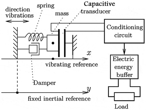
2.1.3. Electrostatic (capacitive) energy harvesting
This type of harvesting is based on the changing capacitance of vibration-dependent varactors. Vibrations separate the plates of an initially charged varactor (variable capacitor), and mechanical energy is converted into electrical energy. Electrostatic generators are mechanical devices that produce electricity by using manual power (Do et al., Citation2013; Qiang et al., Citation2010). The basic operating principle is well explained by Beeby, et al. (Cevik et al., Citation2015) where the harvested energy is provided with work done against the electrostatic force between the plates of the capacitor used. Roundy, et al. (Niu et al., Citation2012; Peters et al., Citation2011) explain the classification of the electrostatic generators into three types which are in-plane overlap, in-plane gap closing and out-of-plane gap closing. The various electrostatic generators under the three different types are discussed in several papers (Başak & Kaçar, Citation2015; Horowitz & Hill, Citation1989). The significant advantage of using the electrostatic converters is their ability to integrate with microelectronics and they do not need any smart material. One of the disadvantages of using electrostatic converters is that they need an additional voltage source to initially charge the capacitor.
Figure 11. Block diagram of main concept of electrostatic harvester.
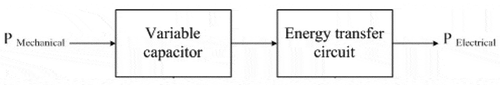
Figure 12. Electrostatic energy harvesting structural-view-of- kinetic-energy-harvester-with-capacitive-interface.
2.1.4. Comparisons between converters of mechanical vibrational energy harvesting
Table shows a Comparisons between Converters of Mechanical Vibration Energy Harvesting: Each of Mechanical Vibration Energy Harvesting converters presents both advantages and drawbacks depending on the application (amplitudes of vibrations, frequencies). A summary of advantages and drawbacks of electrostatic devices is presented in Table .
Table 3. Advantages and drawbacks of converters (Başak & Kaçar, Citation2015)
In most cases, piezoelectric and electrostatic devices are more appropriate for small-scale energy harvesters (<1-10 cm3) while electromagnetic converters are better for larger devices. The electrostatic vibration energy harvesters (VEH) are well adapted for size reduction, increasing electric fields, capacitances and therefore converters’ power density capabilities. They also offer the possibility to decouple the mechanical structure and the converter (which is not possible with piezoelectric devices). Finally, they can be a solution to increase the market of EH-powered WSN by giving the possibility to develop “low-cost” devices as they do not need any magnet or any piezoelectric material that can be quite expensive.
So, the best choice for ES is Electrostatic EH … due to its advantages of high output voltages, low cost systems, high coupling coefficient reachable and easy to adjust, size reduction and increased capacitances. The Electrostatic and Piezoelectric harvesters are capable of producing voltage ranging from 2 to 10 V, whereas the electromagnetic harvesters have a limitation of producing maximum voltage of 0.1 V. The advantage of using mechanical vibrations to harvest energy is that they are the most prevalent energy source available in many environments. The advantage of using mechanical vibrations to harvest energy is that they are the most prevalent energy source available in many environments. Moreover, the output voltage amplitudes of different micro harvesting generators may vary and output power is usually low, and therefore both efficiency and wide range input amplitude are needed for the rectifier design.
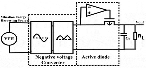
3. Proposed structure of vibrational energy harvesting system
The energy harvesting research falls into two key areas. One is developing optimal structures of energy harvesting and the other is designing electronic circuits that are efficient enough to store the generated charge. Figure shows the schematic of vibrational energy harvesting system design. Regarding the research area of optimal design of electronic circuits, A highly efficient CMOS rectifier for vibrational energy harvesting system is proposed.
Figure 13. Schematic of vibrational energy harvesting system design[39].
![Figure 13. Schematic of vibrational energy harvesting system design[39].](/cms/asset/0307c6cb-138d-4159-95b1-404c217f5b47/oaen_a_1772947_f0013_b.gif)
3.1. Importance of rectifier in the application of energy harvesting system
The Rectifier performance is very important in the whole system design due to several reasons:
1. Voltage efficiency:
The rectifier converts AC voltage supplied by receiver to DC voltage and power delivered to the load circuit. The voltage efficiency of rectifier decides the output voltage. Higher efficiency means larger output voltage;
2. Minimum operation voltage:
The rectifier used in the application must be self-biased. The voltage received from the receiver is not only the rectified signal. The peak amplitude of the input source also influences the output voltage. Inductive coupling between coils or capacitive coupling is the two main technologies for the near field applications. The distance between the two coils and the relative position of coil center influence the transfer efficiency. Farer distance of two coils and the position mismatch of the coil’s center result in small transfer voltage, which means the voltage amplitude received by the receiver will be influenced a lot. Thus, a low voltage rectifier can cover the influence caused by the capacitive coupling or inductive coupling coils mismatch;
3. Power efficiency:
Wireless power transmission system consists of power amplifier, inductive coil, rectifier and regulator. It is important to mention that the efficiency of the rectifier is usually the bottleneck. Higher power efficiency means higher total efficiency;
4. Working frequency:
There are two categories of wireless power techniques, near-field and radiative. The working frequency chosen for the system is also very important. The working frequency should not be too low considering of the coil’s size in the receiver if it is utilized in the biomedical implant devices. However, it should also not be too high for avoiding the potential hazards to human safety. Based on the above considerations, rectifier plays an important role in the application of energy harvesting system and wireless power transfer system. So, the performance of the rectifier decides the efficiency of the system.
3.2. Rectifier topologies
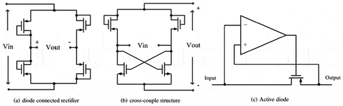
Among several choices for the rectifier in previous publications, full-wave diode rectifier is well known for its simple structure, which is shown in Figure (a). Both schottky diode and diode-connected CMOS transistors can be used in this structure. The performance of these integrated passive rectifiers is less frequency dependent and can be used in some far field applications. However, the voltage and power efficiency are commonly not sufficient because of the two diodes forward voltage drop. In Figure (b), the circuit uses a cross coupled PMOS structure to replace two semiconductor diodes of the diode-bridge structure. Input AC source is directly connected to the gate terminals to drive the PMOS transistors (Pop et al., Citation2007). Comparing with the previous one, the forward voltage drop is reduced to only one Vth (threshold voltage of MOS transistor).
For further increasing the peak voltage conversion efficiency and power efficiency, active diodes for energy harvesting system (Renaud et al., Citation2007; Sterken et al., Citation2007) and wireless power transfer are used instead of the diode configured transistors in the conventional rectifiers. The active diode shown in Figure (c) is composed of a comparator controlled switch working nearly as an ideal diode without voltage drop. When input voltage is larger than the output voltage, the comparator will turn on the switch to charge the load. When input voltage is smaller than the output voltage, the switch will be turned off to block the reverse current from output terminal to input terminal. Higher voltage conversion efficiency and power efficiency can be achieved by replacing the passive diode with active diode. In addition, the minimum input voltage amplitudes are also reduced to under 1 V for the application of vibrational energy harvesting (Renaud et al., Citation2005; Martinez et al., Citation2018).
Figure 14. Full-wave rectifier circuits. (a) diode-connected rectifier, (b) diode-connected rectifier with cross-couple structure, (c) active diode.
However, the performance of these active rectifiers is frequency dependent. Most of them are working below the frequency of 10 kHz, which is only suitable for energy harvesting. In the wireless power transfer system, the operation frequency is very important to the overall system efficiency. Commonly, the size of inductive coils is limited by the system size. Thus, low operation frequency with small size coil will reduce the total power efficiency of the transfer system. For high frequency case, threshold cancellation technologies are commonly used to compensate the passive rectifiers. The idea is to feature a static bias voltage applied between gate and drain terminals of the diode-connected transistor. Comparing with active diodes, passive rectifier with Vth cancellation is less frequency dependent. High voltage conversion efficiency can be achieved by reducing the voltage drop. The Vth cancellation technologies have been proposed and modified. However, the utilization of capacitor increases the chip area and all these circuits are mainly investigated for improving the voltage conversion efficiency and no design strategy has been discussed in terms of reverse current which is first considered in (Sterken et al., Citation2004). Thus, the reverse current is commonly very large in these rectifiers which results in poor power efficiency, especially for low input voltage amplitude. The total efficiency of the wireless power transfer system is also restrained by this poor performance. Though active rectifier is rarely used in higher frequency case, especially in UHF applications, there are still some researches of the active rectifier. The rectifier proposed uses the concept of active diode and is designed for 13.56 MHz. Two common gate structure comparators are connected with each other to improve the operation gain. However, the time delay and reverse current still exist and result in a poor efficiency. In order to overcome the above drawbacks, we present a novel low-voltage rectifier which can work well at high frequency range. In CMOS implementation circuits, MOS transistors in diode configuration (gate connected to the drain) are usually used. In order to achieve high voltage and power efficiency, active diode was presented and can be found in literatures (Qiang et al., Citation2010; Niu et al., Citation2012). The active diode is composed of a comparator controlled MOS transistor switch, working as an ideal diode with current flowing in only one direction and no voltage drop. By using this concept, the minimum input voltage amplitude is further decreased to around 0.45 V (Niu et al., Citation2012). Recently, bulk-input comparator technique is presented in (Peters et al., Citation2011; Qiang et al., Citation2010) for ultralow-voltage systems and the rectifier can work well with input voltage smaller than 1 V. Based on the above consideration, we proposed a high efficiency CMOS rectifier for 13.56 MHz in the readily available (Industrial Scientific Medical) ISM-Band. The rectifier can work with low input voltage amplitude of around 0.45 V. By using two-stage structure and a novel active diode, the rectifier can work at a wide range of input voltage amplitudes of 0.45 V up to 1.95 V in 0.18um CMOS technology. A comparator that consists of common-gate stage and control stage is designed to control the switch of active diode.
3.3. The precision rectifier
It is also known as Active-diode, is a configuration obtained with an operational amplifier to have a circuit behave like an ideal diode and rectifier (Horowitz & Hill, Citation1989). It is very useful for high-precision signal processing. With the help of precision rectifier the high-precision signal processing can be done very easily.
Figure 15. A simple precision rectifier circuit.
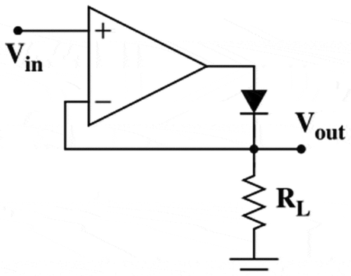
The basic circuit implementing such a feature is shown in Figure . where RL can be any load. When the input voltage is negative, there is a negative voltage on the diode, so it works like an open circuit, no current flows through the load, and the output voltage is zero. When the input is positive, it is amplified by the operational amplifier, which switches on the diode. Current flows through the load and, because of the feedback, the output voltage is equal to the input voltage. The actual threshold of the super diode is very close to zero, but is not zero. It equals the actual threshold of the diode, divided by the gain of the operational amplifier. This configuration has a problem, so it is not commonly used. When the input becomes negative, the operational amplifier runs open-loop, as there is no feedback signal through the diode. For a typical operational amplifier with high open-loop gain, the output saturates. If the input then becomes positive again, the op-amp has to get out of the saturated state before positive amplification can take place again. This change generates some ringing and takes some time, greatly reducing the frequency response of the circuit.
Recently, bulk-input comparator technique is presented in [39], [40] for ultralow-voltage systems and the rectifier can work well with input voltage smaller than 1 V. However, bulk and comparator leakage current increase dramatically when operation voltage is larger than 1 V, which results in a bad performance and limits its scope. In order to overcome these drawbacks, a high efficiency and wide input amplitude range rectifier is presented. The minimum operation voltage is lower than previous published paper and the rectifier can work at a wide range of input voltage amplitudes of 0.45 V up to 1.95 V compared with 0.5 V to 1 V in [39] and 0.28 V to 0.7 V in [40]. This allows the rectifier to work in Different Types of vibration energy harvesting system, Electrostatic harvester, Electromagnetic Energy Harvesting, Piezoelectric Energy Harvester.
The proposed rectifier is consisted of two stages: Negative voltage converter as shown in Figure and comparator controlled active diode. Figure shows the schematic of the two-stage structure. The requirements for the rectifier are defined as follows: i) Wide working voltage range from 0.45 V to 1.95 V; ii) Small leakage current and minimum power consumption lower than 200nW; iii) output voltage conversion efficiency, and the power efficiency. A capacitance of 10uF and load Resistance of 50KΩ are used.
3.4. Negative voltage converter
The first stage of the rectifier is called negative voltage converter and used to convert the negative half cycles of the input sinusoidal wave into positive ones, which is done with two PMOS and two NMOS transistors shown in Figure . During the whole period of the input, node 1 is always the high potential and node 2 is the low potential. Consequently, the bulk of the PMOS transistor can be directly connected to node 1 and the NMOS to node 2. In this case, no voltage drop Vth occurs. The voltage loss is only Vdsp +Vdsn during each conductive branch, where Vdsp and Vdsn are caused by the on-resistance of the transistors. Thus, the dropout voltages can be minimized by using large transistor size to decrease the resistance so as to get a small voltage drop. The simulation results show that the voltage drop in this stage can be less than 10 mV. Though the negative voltage converter has nearly no voltage drop, it cannot control the current direction, therefore, an active diode is necessary to block the reverse current.
Figure 16. Circuit diagram and voltage waveform of negative voltage Converter (Yen & Lang, Citation2006).
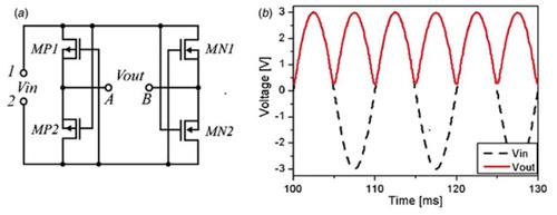
Figure 17. Schematic of the proposed low voltage rectifier.
3.5. Improved precision rectifier circuit
An alternative version is given in Figure ). In this case, when the input is greater than zero, D1 is off, and D2 is on, so the output is zero because the other end of R2 is connected to the virtual ground and there is no current through R2. When the input is less than zero, D1 is on, and D2 is off, so the output is like the input with an amplification of—R2/R1. Its input–output relationship is shown in Figure ). This circuit has the benefit that the op-amp never goes into saturation, but its output must change by two diode voltage drops (about 1.2 V) each time the input signal crosses zero. Hence, the slew rate of the operational amplifier and its frequency response (gain–bandwidth product) will limit high-frequency performance, especially for low signal levels, although an error of less than 1% at 100 kHz is possible.
Figure 18. Improved precision rectifier circuit with low-voltage active diode.
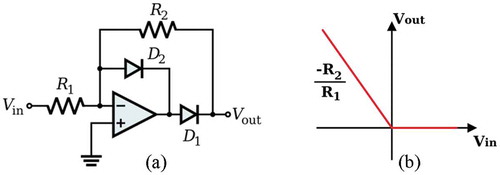
Figure 19. Schematic of the proposed improved rectifier with low-voltage active diode.
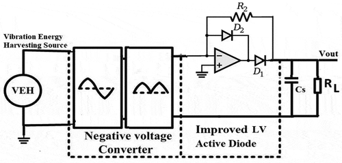
Figure 20. Complete schematic diagram of proposed 0.18um CMOS LV rectifier.
3.6. Simulation results of proposed rectifier using improved precision active diode
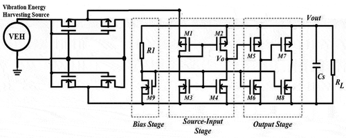
The circuits have been designed in 0.18 um CMOS technology as shown in Figure . Circuits simulations were done using Cadence Tools to optimize the performance and get the required specifications for the proposed system.
3.6.1. Input range and voltage conversion efficiency
The proposed rectifier can work at a wide range of input voltage amplitudes of 0.45 V up to 1.95 V, which is decided by the threshold voltage and breakdown voltage respectively of the standard 0.18um CMOS process. Breakdown voltage verification using cadence Tools is shown in Figure . This wide range of input voltages allows the rectifier to work in different types of vibration energy harvesting system.
Figure 21. Breakdown voltage verification using cadence Tools of standard 0.18um CMOS process.
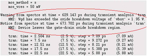
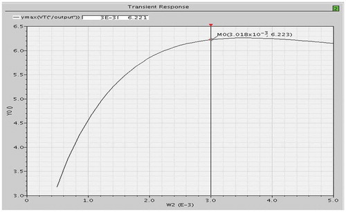
Figure 22. Simulated optimum gate-width of the active-diode is W = 3000um.
The voltage efficiency is defined as the fraction of the output DC voltage Vout and the input voltage amplitude |Vin|, which is shown in EquationEquation (1)(1)
(1) . The output voltage efficiency of the rectifier is higher with larger load resistors due to its high output voltage drop.
3.6.2. Power efficiency of the rectifier is calculated by
where T is one period of the input signal and is the start time. With increasing
, the efficiency decreases, because the current through the ohmic load decreases and tends to the current through the comparator. The load capacitor is adapted for the applied frequency, so a capacitance of 10uF and a load of 50KΩ are used. The voltage efficiency for the lower frequency is better than 1 kHz case. Since higher frequency will results in the delay of the comparator and increasing reverse current. However, at typical energy harvesting frequencies, the working frequency range of this rectifier is sufficient for most applications. The power consumption of the rectifier is simulated. The results show that the power consumption at 0.45 V is 0.23 uW, which is about 30% smaller than the best recently published result.
4. Performance comparisons
Table shows the performance comparisons of this work with other previously reported rectifiers. The lowest operation voltage of previous rectifiers is 0.5 V in (Niu et al., Citation2012) with a 500 mV low threshold voltage 0.35um CMOS process. However, it cannot work when the input voltage is larger than 1 V, which blocks the application field. The rectifier proposed in this paper overcome these drawbacks. It can not only work at a 0.45 V input voltage but also operate at a wide range input voltage amplitudes of 0.45 V up to 1.95 V compared with 0.5 V to 1 V in (Niu et al., Citation2012) and 0.28 V to 0.7 V in (Peters et al., Citation2011) (Başak & Kaçar, Citation2015)
Table 4. Performance parameters comparisons between low voltage rectifiers
In this paper, a wide range input voltage amplitude and highly efficient rectifier for energy harvesting system was proposed. The rectifier is well suited for an input amplitude as low as 0.45 V and can work at a wide range of input voltage amplitudes of 0.45 V up to 1.95 V under a standard 0.18um CMOS process. The proposed rectifier can achieve peak voltage conversion efficiency of over 81% and power efficiency over 79%. Simulated power consumption of the rectifier is 0.23 uW at 0.45 V, which is about 28% smaller than the best recently published results.
5. Conclusions
Performance improvements in battery technology and the power requirements of electronics are not keeping pace with the increasing demands of many wireless sensor networking applications. For this reason, there has been considerable interest in the development of systems capable of extracting usable electrical energy from existing environmental sources. Such sources include ambient electromagnetic energy, thermal gradients, vibration and other forms of motion. The energy harvesting research falls into two key areas. One is developing optimal structures of energy harvesting and the other is designing electronic circuits that are efficient enough to store the generated charge. So Regarding the designing of electronic circuits, the optimum Performance of Energy Harvesting Solutions for 0.18um CMOS Circuits in Embedded Electronics Design is achieved by Low Voltage Rectifier using improved precision active diode. The proposed rectifier is designed for 13.56 MHz using two-stage structure and an improved precision active diode under a standard 0.18um CMOS process can perform the minimum operation voltage is lower than previous published paper and the rectifier can work at a wide range of input voltage amplitudes of 0.45 V up to 1.95 V. This allows the proposed rectifier to work in Different Types of vibration energy harvesting system, Electrostatic Energy harvester., Electromagnetic Energy Harvester, piezoelectric Energy Harvester. The proposed rectifier can achieve peak voltage conversion efficiency of over 81% and power efficiency over 79%. Simulated power consumption of the rectifier is 0.23 uW at 0.45 V, which is about 28% smaller than the best recently published results. The advantage of using mechanical vibrations to harvest energy is that they are the most prevalent energy source available in many environments.
Cover image
Source: Author.
Additional information
Funding
Notes on contributors
Hafez Fouad
Hafez Fouad, Ph.D was born in EGYPT 1971, has 27 years of experience in fields of electronics industry of Embedded systems, trade and economy, he received many degrees in scientific, industrial, technological, economic, strategic, organizational and administrative skills since graduating from the Faculty of Engineering in 1993. The National Strategy, National Security and State Administration Sciences at Nasser Higher Military Academy, Ministry of Defense. Economics and Business Administration at Ain Shams University, International Arbitration Studies in Investment Disputes, Foreign Relations and Diplomacy in Faculty of Law, Ain Shams University, Diploma Studies in International Negotiations, Public Policies, Parliamentary Organizations, and Civil Society, Faculty of Economics and Political Science, Cairo University. He is working since 1994 at National Electronics Research Institute in Ministry of Scientific Research and Technology and published more than 68 research papers, scientific, technical and technological reports in international conferences and periodicals and technical committees. He was a Board Member at Federation of Egyptian Industries and Chairman of Arabic Industries Informatics Network since 2003.
References
- Anton, S. R., & Sodano, H. A. (2007). A review of power harvesting using piezoelectric materials (2003–2006). Smart Materials and Structures, 16(3), R1. https://doi.org/10.1088/0964-1726/16/3/R01
- Başak, M. E., & Kaçar, F. (2015). A new fully integrated high frequency fullwave rectifier realization. Journal of Microelectronics, Electronic Components and Materials, 45(2), 101–23. http://www.midem-drustvo.si/Journal%20papers/MIDEM_45(2015)2p101.pdf
- Cevik, I., Huang, X., Yu, H., Yan, M., & Ay, S. U. (2015). An ultra-low power CMOS image sensor with on-chip energy harvesting and power management capability. Sensors, 15(3), 5531–5554. https://doi.org/10.3390/s150305531
- Cook, B. W., Lanzisera, S., & Pister, K. S. J. (2006). SoC issues for RF smart dust. Proceedings of the IEEE, 94(6), 1177–1196. https://doi.org/10.1109/JPROC.2006.873620
- Din, A. U., Chung, D., Park, D., Lee, H., & Lee, J.-W. 2014. A high extraction self-controllable CMOS resonant rectifier circuit for piezoelectric energy scavenging system. In Proceedings of the 2014 International SoC Design Conference (ISOCC), 3–6 November pp. 40–41.
- Do, X.-D., Nguyen, H. H., Han, S. K., & Lee, S.-G. 2013. A rectifier for piezoelectric energy harvesting system with series synchronized switch harvesting inductor. In Proceedings of the 2013 IEEE Asian solid-state circuits conference (A-SSCC), 11–13 November pp. 10–13.
- Gilbert, J. M., & Balouchi, F. (2018, October). Comparison of energy harvesting systems for wireless sensor networks. International Journal of Automation and Computing, 5(4), 334–347. https://doi.org/10.1007/s11633-008-0334-2
- Guo, S., & Lee, H. (2009). An efficiency-enhanced CMOS rectifier with unbalanced-bias comparators for transcutaneous power high-current implants. IEEE Journal of Solid-State Circuits, 44(6), 1796–1804. https://doi.org/10.1109/JSSC.2009.2020195
- Horowitz, P., & Hill, W. (1989). The art of electronics (2nd ed.). Cambridge University Press.
- Jin, W., Wang, Z., Huang, H., Hu, X., He, Y., Li, M., Li, L., Gao, Y., Hu, Y., & Gu, H. (2018). High-performance piezoelectric energy harvesting of vertically aligned Pb(Zr,Ti)O3 nanorod arrays. RSC Advances, 8(14), 7422–7427. https://doi.org/10.1039/C7RA13506H
- Kamarudin, S., Daud, W., Ho, S., & Hasran, U. (2007). Overview on the challenges and developments of micro-direct methanol fuel cells (DMFC). Journal of Power Sources, 163(2), 743–754. https://doi.org/10.1016/j.jpowsour.2006.09.081
- Kwon, D., & Rincón-Mora, G. A. F. (2014). A single-inductor 0.35 m CMOS energy-investing piezoelectric harvester. IEEE Journal of Solid-State Circuits, 49(10), 2277–2291. https://doi.org/10.1109/JSSC.2014.2342721
- Li, P., & Bashirullah, R. (2017, October). A wireless power interface for rechargeable battery operated medical implants. IEEE Transactions on Circuits and Systems II, Exp.Briefs, 54(10), 912–916. https://doi.org/10.1109/TCSII.2007.901613.
- Lu, C., Tsui, C. Y., & Ki, W. H. (2011). Vibration energy scavenging system with maximum power tracking for micropower applications. IEEE Transactions on Very Large Scale Integration (VLSI) Systems, 19(11), 2109–2119. https://doi.org/10.1109/TVLSI.2010.2069574
- Lu, C., Tsui, C. Y., & Ki, W. H. 2017. Vibration energy scavenging and management for ultra low power applications. In Proceedings of the ACM/IEEE international symposium on low power electronics and design (ISLPED), 27–29 August; pp. 316–321.
- Martinez, T., Pillonnet, G., & Costa, F. (2018). A 15-mV Inductor-less start-up converter using a piezoelectric transformer for energy harvesting applications. IEEE Transactions on Power Electronics, 33(3), 2241–2253. https://doi.org/10.1109/TPEL.2017.2690804
- Mitcheson, P. D., Green, T. C., Yeatman, E. M., & Holmes, A. S. (2004). Architectures for vibration driven micropower. Journal of Microelectromechanical Systems, 13(3), 429–440. https://doi.org/10.1109/JMEMS.2004.830151
- Mitcheson, P. D., Yeatman, E. M., Rao, G. K., Holmes, A. S., & Green, T. C. (2008). Energy harvesting from human and machine motion for wireless electronic devices. Proceedings of the IEEE, 96(9), 1457–1486. https://doi.org/10.1109/JPROC.2008.927494
- Niu, D., Huang, Z., Jiang, M., & Inoue, Y. (2012, July). A Sub-0.3V highly efficient CMOS rectifier for energy harvesting applications. Ieice Nolta, 3(3), 405–416. https://doi.org/10.1587/nolta.3.405
- Ottman, G. K., Hofmann, H. F., Bhatt, A. C., & Lesieutre, G. A. (2012, September). Adaptive piezoelectric energy harvesting circuit for wireless remote power supply. IEEE Transactions on Power Electronics, 17(5), 669–676. https://doi.org/10.1109/TPEL.2002.802194
- Peters, C., Handwerker, J., Maurath, D., & Manoli, Y. (2011, July). A sub-500 mV highly efficient active rectifier for energy harvesting applications. IEEE Transactions on Circuits and Systems I: Regular Papers, Reg. Papers, 58(7), 1542–1550. https://doi.org/10.1109/TCSI.2011.2157739.
- Pop, V., Bergveld, H. J., Notten, P. H. L., Regtien, P. P. L., Op Het Veld, J. H. G., & Danilov, D. (2007). Battery aging and its influence on the electro-motive force. Journal of the Electrochemical Society, 154(8), A744–50. https://doi.org/10.1149/1.2742296
- Qiang, L., Zhang, R., Huang, Z., & Inoue, Y. 2010 A low Voltage CMOS rectifier for wirelessly powered devices. IEEE international symposium on circuits and systems, pp.873–876, May
- Raghunathan, V., Kansal, A., Hsu, J., Friedman, J., & Srivastava, M. B. 2015. Design considerations for solar energy harvesting wireless embedded systems. Proc. IPSN, Apr. 25–27, pp. 457–462.
- Renaud, M., Fiorini, P., & Van Hoof, C. (2007). Optimization of a piezoelectric unimorph for shock and impact energy harvesting. Smart Materials and Structures, 16(4), 1125–1135. https://doi.org/10.1088/0964-1726/16/4/022
- Renaud, M., Sterken, T., Fiorini, P., Puers, R., Baert, K., & Van Hoof, C. 2005. Harvesting energy from human-body: Design of a piezoelectric transducer. In: Proceedings of the 13th int conf on solid–state sensors, actuators and microsystems, transducers 2005. p. 784–787.
- Sauer, C., Stanac´evic´, M., Cauwenberghs, G., & Thakor, N. (2015, December). Power harvesting and telemetry in CMOS for implanted devices. IEEE Transactions on Circuits and Systems I, Reg. Papers, 52(12), 2605–2613. https://doi.org/10.1109/TCSI.2005.858183.
- Shenck, N. S., & Paradiso, J. A. (2001). Energy harvesting with shoe-mounted piezoelectrics. IEEE Micro, 21(3), 30–42. https://doi.org/10.1109/40.928763
- Siddiqui, S., Lee, H. B., Kim, D. I., Duy, L. T., Hanif, A., & Lee, N. E. (2018). An omnidirectionally stretchable piezoelectric nanogenerator based on hybrid nanofibers and carbon electrodes for multimodal straining and human kinematics energy harvesting. Advanced Energy Materials, 8(2), 1701520. https://doi.org/10.1002/aenm.201701520
- Sterken, T., Baert, K., Van Hoof, C., Puers, R., Borghs, G., & Fiorini, P. 2004. Comparative modeling for vibration harvesters. In: Proceedings of IEEE sensors conference. p. 1249–1252.
- Sterken, T., Fiorini, P., Baert, K., Puers, R., & Borghs, G. 2003. An electret-based electrostatic micro-generator. In: Proceedings of the 12th int conf on solid-state sensors, actuators and microsystems transducers. p. 1291–1294.
- Sterken, T., Fiorini, P., & Puers, R. (2007). Motion-based generators for industrial applications. In Proceedings of international conference on design, test, integration and packaging of MEMS/MOEMS; 2007 (pp. 328–331). Stresa, Italy.
- Sun, Y., Hieu, N. H., Joeng, C. J., & Lee, S. G. (2012). An integrated high-performance active rectifier for piezoelectric vibration energy harvesting system. IEEE Transactions on Power Electronics, 27(2), 623–627. https://doi.org/10.1109/TPEL.2011.2162078
- Torfs, T., Leonov, V., & Van Hoof, C. 2006. Bert gyselinckx body-heat powered autonomous pulse oximeter. In: 5th IEEE conference on sensors. p. 427–430.
- Yen, B. C., & Lang, J. H. (2006, February). A variable-capacitance vibration-to-electric energy harvester. IEEE Transactions on Circuits and Systems I, Reg. Papers, 53(2), 288–295. https://doi.org/10.1109/TCSI.2005.856043.
- Yildiz, F. (2007). Potential Ambient Energy-Harvesting Sources and Techniques. J. Technol. Stud. 40–48.
- Zhao, T., Fu, Y., He, H., Dong, C., Zhang, L., Zeng, H., Xing, L., & Xue, X. (2018). Self-powered gustation electronic skin for mimicking taste buds based on piezoelectric–enzymatic reaction coupling process. Nanotechnology, 29(7), 075501. https://doi.org/10.1088/1361-6528/aaa2b9