
ABSTRACT
In recent years, taking advantages of high light absorption coefficients, long charge carrier diffusion lengths and intense photoluminescence, halide perovskites have attracted a great deal of interest in developing high-performance optoelectronic devices including solar cells, light-emitting diodes, photodetectors, transistors, lasers, and so on. Especially, the excellent combination of effective light absorption with tailorable absorption spectrum and high charge carrier mobility in a broadband range makes perovskite-based photodetectors different from traditional photodetectors made of inorganic semiconductors such as GaN, Si, and InGaAs. According to the recent reports, perovskites are promising to greatly improve responsivity, detectivity, noise equivalent power, linear dynamic range, and response speed of photodetectors. Here, we summarize the recent advancements in organic–inorganic hybrid perovskite-based photodetectors in terms of the progress in various low-dimension perovskites, and the recent effective approaches to enhance the performance of perovskite photodetector based on the interfacial engineering in perovskite heterostructures. Besides, two kinds of perovskite photodetectors, namely vertical structure and lateral structure, are analyzed, and the challenges to achieve practical applications in photodetectors are also discussed.
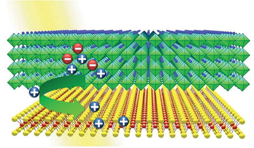
GRAPHICAL ABSTRACT
1. Introduction
Photodetectors are the devices which can convert incident light into an electrical signal via the photoelectric effect. Nowadays, photodetectors are crucial for a variety of industrial and scientific applications, including imaging sensing, optical communications, environmental monitoring, and chemical/biological sensing [Citation1–Citation4]. The primary photodetectors are made of inorganic semiconductors such as GaN, Si, and InGaAs [Citation5]. However, as for these traditional photodetectors which possess the mature and reliable fabrication processes and technologies, their development is hampered by the complex and expensive manufacture, mechanical inflexibility and high driving voltage. Recently, solution-processable optoelectronic materials, such as organic-inorganic hybrid perovskite materials with a typical formula of ABX3 (A = MA, FA, et al.; B = pb, Sn, et al.; X = Cl, Br, I) have attracted wide research interests owing to their direct bandgaps, long-range electron and hole transport lengths, and high absorption coefficients. These unique features render perovskites unique electrical and optoelectronic properties in low-cost, flexible optoelectronic devices [Citation6–Citation8].
The organometal halide perovskite materials with layered structure take the advantages of inorganic semiconductor materials and organic materials simultaneously, and the cooperation of these two components could greatly enhance the properties for each other. On one hand, they show ultrafast charge generation, high mobility, and long charge carrier lifetime, which is attributed to the inorganic material. On the other hand, they enjoy the organic properties of easy fabrication and no deep-level defects [Citation9]. To begin with, organometal halide perovskites as visible-light sensitizers have been considered for photovoltaic cells [Citation10]. By building on pioneering advances in mesoscopic dye-sensitized solar cells, rapid progresses have been made in solar cells [Citation11–Citation15]. Researchers have greatly increased the efficiency of perovskite photovoltaics from about 3% to 23.2% in only several years of active research [Citation16]. The rapid and impressive progress in perovskite solar cell field has also aroused the exploration of the application in other optoelectronic devices including perovskite LEDs [Citation17–Citation20], transistors, photodetectors [Citation21–Citation23], lasers [Citation24,Citation25], and so on. Ultrathin perovskite layers and small perovskite grain size have been employed to spatially confine electrons and holes to promote bimolecular radiative recombination [Citation26–Citation29]. The external quantum efficiency (EQE) of organic-inorganic hybrid perovskite LEDs was first reported to be 0.76% [Citation30] and experienced a tremendous upgrade to exceeding 20% within several years [Citation31,Citation32].
Perovskites have large optical absorption coefficient over a broad wavelength range from 300 to 800 nm (ultraviolet, visible, and infrared), which is desirable for applications in broadband photodetectors [Citation33]. The excellent combination of effective light absorption with tailorable absorption spectrum and high charge carrier mobility in a broadband range of perovskites makes them different from other photosensitive materials used in photodetectors. Therefore, the organic-inorganic hybrid perovskite is a promising candidate for photodetectors due to their excellent optical and electronic properties, which are expected to improve responsivity, detectivity, noise equivalent power, linear dynamic range, and response speed of photodetectors [Citation34].
In this paper, we review the recent advancements in organic–inorganic hybrid perovskite-based photodetectors. The article begins with the introduction of recent progress in various low-dimension perovskite photodetectors. In addition, we highlight the recent effective approaches to enhance the performance of perovskite photodetectors based on interfacial engineering in perovskite heterostructures. Besides, two kinds of perovskite photodetectors, namely vertical and planar structure, are compared and discussed. Finally, the possible research directions and challenges in perovskite-based photodetectors are proposed.
2. Low dimensional perovskite materials for photodetectors
The performance of photodetector is strongly influenced by the separation mechanism and transport properties of photon-generated carriers [Citation11]. Therefore, it is possible to improve the performance of photodetector by elevating the exciton separation efficiency and selective charge trapping to maximize the trapping time. The perovskites with a low dimensional geometry possess a lot of advantages such as reduced defect density and improved charge-carrier mobility, which are beneficial for harvesting charges induced by photons [Citation33]. Moreover, the low dimensional perovskite structures have a greatly reduced channel thickness, which is also critically important for obtaining much smaller dark currents [Citation35].
2.1. 0D nanocrystals perovskite photodetectors
All-inorganic perovskites nanocrystals (CsPbBr3) gain more and more attentions in photodetectors because of their outstanding optoelectronic properties [Citation36,Citation37]. Meanwhile, PC71BM as an organic semiconductor is used for photodetectors with CsPbBr3 nanocrystals, which can enhance the spectral absorption range and intensity, thereby increasing the rate of exciton generation. Tengteng Li research group [Citation33] fabricated hybrid perovskite-organic photodetector by integrating CsPbBr3 nanocrystals with PC71BM, exhibiting remarkable optoelectronic properties in terms of photoresponsivity (1.72 AW−1), detectivity (1.76 × 10⁷ Jones), EQE (530%) (). Besides, the photoresponse time is shorter than 0.1 ms due to the assistance of heterojunction on the separation of photoexcitons. Because the photon energy (3.10 eV) was larger than the band gaps of CsPbBr3 nanocrystals (2.3eV) and PC71BM (2.4eV), a large number of charges would be generated in the active layer. These charge pairs were quickly dissociated near the interface by driving bias, and then the electrons transferred from CsPbBr3 nanocrystals to PC71BM. Besides, PC71BM provided electron trapping sites [Citation34], which were favorable for the separation of electrons and holes, thus reducing the recombination of the charge carriers efficiently and inducing enhanced photocurrent and faster photoresponse.
Figure 1. (a) Device schematic diagram. (b) The energy level diagram of the CsPbBr3-PC71BM bilayer photodetector under the illumination of hν > 2.3 eV. Photodetector performances of EQE (c) and photodetectivity (d) with the relationship of light irradiance, respectively [Citation33]. Copyright from 2018 Chem. Phys. Lett.
![Figure 1. (a) Device schematic diagram. (b) The energy level diagram of the CsPbBr3-PC71BM bilayer photodetector under the illumination of hν > 2.3 eV. Photodetector performances of EQE (c) and photodetectivity (d) with the relationship of light irradiance, respectively [Citation33]. Copyright from 2018 Chem. Phys. Lett.](/cms/asset/68993903-5b33-4f88-a3a5-1b27d2e97441/tapx_a_1592709_f0001_oc.jpg)
2.2. 1D nanocrystals perovskite photodetectors
Similar to the 0D perovskites nanocrystals, one-dimensional (1D) perovskite materials are also promising for the application in photodetectors because of their high sensitivity, rapid response time, reduced recombination rate, which can be applied as ideal building blocks to construct high-performance photodetectors. Jong Hyeok Park research group [Citation35] developed vertically grown halide perovskite (VGHP) nanopillar photodetectors via a nanoimprinting crystallization technique. The NH3PbI3 VGHP photodetector showed improved performance in terms of photophysical and electronic properties over the flat film-based photodetector, leading to high responsivity and detectivity ()). The authors found that the dark current (Idark) of the VGHP photodetectors was lower than that of the reference devices, which could be explained by the reduced channel thickness (~130 nm) and decreased defect density [Citation38,Citation39]. The reduced defect density extended the carrier diffusion length and enhanced the charge-carrier mobility [Citation40]. Besides, the photocurrent (Iphoto) increased due to the enhanced light absorption and high-quality crystallization of CH3NH3PbI3, inducing a dramatic enhancement in the photocurrent [Citation10,Citation41–Citation45]. These results indicated directly that the performance of the photodetector under illumination can be improved through suppressing the nonradiative recombination in the perovskite film. With the help of the nanopillar structure of the VGHP channel, the responsivity and detectivity of the VGHP devices increased to approximately 1 AW−1 and 5 × 10⁹ Jones ()), respectively, which could be attributed to both the increased Iphoto and suppressed Idark. The on/off current ratio increased with optical power and was over 100. The rise and fall times were found to be less than 100 ms which could be attributed to the improved charge-carrier mobility.
Figure 2. (a) Schematic illustration of the VGHP photodetectors. (b) Responsivity and detectivity of the reference and VGHP photodetectors [Citation35]. Copyright from 2018 ACS Nano. (c) The SEM image of the nanowires and time response behavior of reversible on/off switching for HPNW-based photodetectors. (d) The detectivity performance of HPNW-based photodetectors fabricated with PbI2 molar ratios of 0.4 M and 0.8 M devices [Citation46]. Copyright from 2018 Nano Energy. (e) Schematic illustration of CH3NH3PbI3 NW array photodetector. (f) Plots of responsivity and photoconductive gain of the photodetector as a function of light wavelength [Citation49]. Copyright from 2017 Nano Lett.
![Figure 2. (a) Schematic illustration of the VGHP photodetectors. (b) Responsivity and detectivity of the reference and VGHP photodetectors [Citation35]. Copyright from 2018 ACS Nano. (c) The SEM image of the nanowires and time response behavior of reversible on/off switching for HPNW-based photodetectors. (d) The detectivity performance of HPNW-based photodetectors fabricated with PbI2 molar ratios of 0.4 M and 0.8 M devices [Citation46]. Copyright from 2018 Nano Energy. (e) Schematic illustration of CH3NH3PbI3 NW array photodetector. (f) Plots of responsivity and photoconductive gain of the photodetector as a function of light wavelength [Citation49]. Copyright from 2017 Nano Lett.](/cms/asset/8fd5c446-4cba-4cb4-a903-30e0eebb26b7/tapx_a_1592709_f0002_oc.jpg)
The use of an intertwined perovskite nanowire network could also facilitate the fabrication and the scaling, while significantly improving the photodetector performance due to a larger surface-to-volume ratio. Sylvain G. Cloutier research group [Citation46] presented a simple, fast and low-cost all-solution fabrication technique to produce lead-halide perovskite nanowire-based photodetectors in ambient air. The MAPbI3-x(SCN)x photodetectors exhibited the fast response and recovery times close to 53.2 µs and 50.2 µs, high-specific detectivity of 7.1 × 10¹¹ Jones, together with excellent performance stability for more than 500 h ()). The devices required no charge collectors, which reduced fabrication steps and costs because of the particular 1D perovskite nanowire morphology. And 1D nature of the perovskite nanowires could facilitate the charge transport to the electrodes, synergetically reducing the response time. The single-crystalline perovskite nanowires (NWs) with well-defined structures possess higher photoluminescence (PL) quantum yields, larger carrier mobilities, and longer carrier diffusion lengths [Citation47,Citation48]. Jiansheng Jie research group [Citation49] demonstrated a proof of concept device for wavelength measurement by integrating the perovskite nanowire arrays with tunable bandgap. Using NH3Pb(I1−xBrx)3 nanowire arrays of varying I/Br ratio, they realized broadband photodetectors with a sequentially tunable spectral response. Importantly, the nanowire arrays showed similar responsivity values when x is tuned in the range of 0−0.4 except for the different wavelength response range, which was beneficial to device integration. Furthermore, the range and resolution of wavelength measurement may be further increased by selecting different halogen atoms (Cl, Br, I) or fine-tuning the ratio of halogen atoms in the perovskite nanowires [Citation50]. Photodetectors made of the perovskite nanowire arrays exhibited an extremely high responsivity of 12,500 AW−1. Additionally, other key figure-of-merit parameters of the photodetectors were obtained, such as 3 dB bandwidth (0.8 MHz), detectivity (1.73 × 10¹¹ Jones), and linear dynamic range (150 dB) ()). Furthermore, the monolithic integration of these photodetectors offered a unique capability to directly measure light wavelength.
2.3. 2D nano-sheet/plate crystals photodetectors
Two-dimensional (2D) ordered nanostructure arrays have attracted intensive attention in the fields of photonics, electronics, sensing, solar energy conversion, and optoelectronic devices due to their excellent pattern-dependent properties [Citation51–Citation54]. And the high-quality 2D perovskite platelets can be obtained on random substrates, especially on transparent, flexible, and lower melting point substrates which would greatly extend the photodetector applications. Shaojuan Li research group [Citation55] prepared high-quality 2D CH3NH3PbI3 perovskite platelets by a two-step method. The thicknesses of 2D perovskites platelets could be modified from hundreds of nanometers to a single unit cell (2 nm) on different substrates ()). It was found that the thicker perovskite platelet has a higher PL wavelength and stronger PL intensity. The 2D perovskite platelet photodetectors exhibited a high photoresponsivity of 8.3 AW− 1, a high on/off ratio of ~103 with a small rise and a decay time of 30 and 50 ms, respectively ()). Shaojuan Li research group [Citation56] fabricated a high-performance vertical photodetector based on 2D CH3NH3PbI3 perovskite nanosheets, which possessed low trap density and short carrier diffusion distance. The photoresponsivity of this vertical structure photodetector could reach 36 mA W−1 at a visible wavelength. Compared with traditional planar structure perovskite-based photodetectors, this vertical structure photodetector also showed the advantages of low-voltage operation and large responsivity ()). The unique CH3NH3PbI3 nanonets consisting of large crystal grains exhibited significantly enhanced photoresponsive performance owing to the unique architecture that is beneficial to light harvesting and charge collection. Limin Qi research group [Citation57] fabricated novel CH3NH3PbI3 nanonets and nanobowl arrays facilely by using monolayer colloidal crystal (MCC) templates on the coarse FTO substrate. Particularly, the nanonet photodetectors exhibited a high responsivity of 10.33 AW−1 under 700 nm, fast response speed, and good stability ()). The CH3NH3PbI3 nanonets exhibited an enhanced light harvesting ability and offered direct carrier transport pathways owing to the 2D arrayed structure. These results may pave the way for exploiting high-performance perovskite-based photodetectors with an ingenious device design.
Figure 3. (a) Schematic of a 2D CH3NH3PbI3 platelet phototransistor. The upright inset showed the optical microscopy image of the 2D CH3NH3PbI3 platelet phototransistor. (b) Dependence of photocurrent and photoresponsivity on incident light power, the blue and black dots correspond to original data [Citation55]. Copyright from 2018 Nanomaterials. (c) Schematic image of the CH3NH3PbI3 vertical structure photodetector looking through the back side of the glass substrate. (d) The band alignment for the ITO/perovskite/Au vertical heterostructure [Citation56]. Copyright from 2017 J. Phys. D. (e) Schematic illustration of the mechanism of perovskite nanonet photodetector. (f) I–t curves of the CH3NH3PbI3 photodetectors based on nanonet and compact film illuminated under monochromatic light at 700 nm [Citation57]. Copyright from 2017 Adv. Funct. Mater.
![Figure 3. (a) Schematic of a 2D CH3NH3PbI3 platelet phototransistor. The upright inset showed the optical microscopy image of the 2D CH3NH3PbI3 platelet phototransistor. (b) Dependence of photocurrent and photoresponsivity on incident light power, the blue and black dots correspond to original data [Citation55]. Copyright from 2018 Nanomaterials. (c) Schematic image of the CH3NH3PbI3 vertical structure photodetector looking through the back side of the glass substrate. (d) The band alignment for the ITO/perovskite/Au vertical heterostructure [Citation56]. Copyright from 2017 J. Phys. D. (e) Schematic illustration of the mechanism of perovskite nanonet photodetector. (f) I–t curves of the CH3NH3PbI3 photodetectors based on nanonet and compact film illuminated under monochromatic light at 700 nm [Citation57]. Copyright from 2017 Adv. Funct. Mater.](/cms/asset/b9ab7eb1-0785-4ad4-8508-ec393fdedc1b/tapx_a_1592709_f0003_oc.jpg)
The perovskite materials with low dimensional geometry possess advantages as follows: i) Improved charge-carrier mobility and direct carrier transport pathway, which can lead to rapid response time; ii) Reduced channel thickness which is critically important for obtaining much smaller dark current and higher detectivity; iii) Large surface-to-volume ratio and high-quality crystallization, which facilitate the progress of responsivity.
3. Perovskite heterostructure-based photodetectors
The combined characteristics of high responsivity and detectivity, fast response speed, and broad spectral response are always the pursuits of researchers on the study of photodetectors. As known, three aspects are required in the trap-assisted photoamplification mechanism as follows: i) photogenerated carriers; ii) interface-trapped carriers yield when the photogenerated electrons and holes drift to the respective electrodes; and then iii) the interface-trapped carriers triggering the injection or tunneling of opposite charge carriers. Through this mechanism, the trapping of one type of charge carrier at the semiconductor/electrode interface and the injection of opposite charges from the corresponding electrode can dramatically boost the EQE and gain in perovskite photodetectors. It has been demonstrated that the photogenerated charges can be effectively separated by the interface engineering, thus reducing the charge recombination and prolong the lifetime of carriers, which will contribute to higher responsivity and EQE. Furthermore, it is possible to extend the response spectra of perovskite devices from ultraviolet range to the near-infrared region by integrating perovskite with other narrow-bandgap materials possessing appropriate band alignment.
3.1. 0D nanostructures/perovskite photodetectors
One of the best candidates for extending the response spectra of perovskite is introducing quantum dots which take advantages of high quantum efficiencies and the ability to easily tune their bandgap by controlling their size [Citation58]. Riad Nechache research group [Citation59] have successfully combined single-wall carbon nanotubes (SWCNT), PbS quantum dots (QDs) and perovskite to synthesize hybrid devices, which are suitable for the fabrication of ultra-broadband and highly sensitive high-speed photodetectors ()). The results showed that the presence of the PbS QDs on the SWCNT further promoted the charge transfer from the perovskite to the SWCNT, and the responsivity of photodetector reached the value of 0.5 AW−1 at 500 nm with an applied bias of 1 V. Additionally, the spectral shape of the photocurrent response showed that the photocurrent peak in the near-infrared region shifted to longer wavelengths as the QD size increased. On decreasing the QD size, more charges transferred and then higher photocurrent was obtained, which could be explained by the generation of multiple excitons. Moreover, the incorporation of nanotubes within the perovskite matrix facilitates the carrier extraction, resulting in response time under 250 µs, a gain-bandwidth product of 0.1 MHz and detectivities of 1.4 × 10¹¹ Jones and 0.9 × 10¹¹ Jones at 500 nm and at 1300 nm, respectively. These performances were attributed to the high mobility of combined film due to the SWCNTs, combined with the added contribution of the PbS QDs to boost the charge transfer. Zhigang Zang research group [Citation60] fabricated ITO/CsPbBr3:ZnO/Ag sandwich-structured photodetectors, in which the uniform and compact CsPbBr3 crystalline films were facilitated by introducing ZnO nanoparticles. The effective area of the CsPbBr3:ZnO device for absorbing light was larger than that of the controlled CsPbBr3 device, and correspondingly the number of photogenerated electron-hole pairs increased, while the short-circuit current decreased ()). Owing to the energy level matching of the ZnO NPs and the CsPbBr3 film, the photogenerated electrons can transfer to the ZnO NPs rapidly, and the carrier recombination was greatly prohibited. On the other words, the decoration of the ZnO NPs in the CsPbBr3:ZnO device led to the fast transfer of the photogenerated electron-hole pairs, which was described experimentally by the improved photocurrent of the CsPbBr3:ZnO device. Therefore, both the response speed and the responsivity of the CsPbBr3:ZnO device were enhanced.
Figure 4. (a) Photocurrent spectra of different SWCNT/PbS-QDs hybrid devices made with QDs of different sizes, showing the responses in the NIR which can be tuned by varying the PbS-QDs size. (b) Comparison between the photocurrent and the corresponding responsivity of the SWCNT/MAPbI3-xClx hybrid and of the SWCNT/PbS-QDs/MAPbI3-xClx hybrid photodetectors as a function of the illumination power of a 980 nm laser. (c) Responsivity and photoconductive gain of the SWCNT/PbS-QDs/MAPbI3-xClx hybrid fabricated with PbS-QDs of 4.95 nm diameter measured with lamp power 10 times at 1 V [Citation59]. Copyright from 2018 Nanoscale. (d) Schematic diagram of energy levels of the CsPbBr3:ZnO photodetectors. (e) I–V curves of CsPbBr3:ZnO photodetectors. Insets showed the zoomed-in areas. (f) Photoresponse of the CsPbBr3:ZnO devices with external bias [Citation60]. Copyright from 2017 Sol. Energ. Mat. Sol. C.
![Figure 4. (a) Photocurrent spectra of different SWCNT/PbS-QDs hybrid devices made with QDs of different sizes, showing the responses in the NIR which can be tuned by varying the PbS-QDs size. (b) Comparison between the photocurrent and the corresponding responsivity of the SWCNT/MAPbI3-xClx hybrid and of the SWCNT/PbS-QDs/MAPbI3-xClx hybrid photodetectors as a function of the illumination power of a 980 nm laser. (c) Responsivity and photoconductive gain of the SWCNT/PbS-QDs/MAPbI3-xClx hybrid fabricated with PbS-QDs of 4.95 nm diameter measured with lamp power 10 times at 1 V [Citation59]. Copyright from 2018 Nanoscale. (d) Schematic diagram of energy levels of the CsPbBr3:ZnO photodetectors. (e) I–V curves of CsPbBr3:ZnO photodetectors. Insets showed the zoomed-in areas. (f) Photoresponse of the CsPbBr3:ZnO devices with external bias [Citation60]. Copyright from 2017 Sol. Energ. Mat. Sol. C.](/cms/asset/aadfa689-51b8-41d8-9d64-ce4dae338589/tapx_a_1592709_f0004_oc.jpg)
3.2. 1D nanostructures/perovskite photodetectors
The electron transport in 1D nanostructure has been thought to be several orders of magnitude faster than that of nanoparticles due to the reduced scattering effect from the grain boundaries [Citation61–Citation63]. Carbon nanotubes (CNTs), which are good candidates for carrier transport layers and electrodes, have been widely used in perovskite devices to obtain the optimized performance taking advantages of their outstanding electronic and mechanical properties. WeiLong Xu research group [Citation64] explored the photophysical dynamics and carrier transport of composites of perovskite and CNTs ()). The results showed that the charge transfer from perovskite to carbon nanotubes at the interface by spatially and temporally resolved fluorescence measurements. Carbon nanotubes served as the effective charge transport pathways to improve the performance of photodetector by reducing the grain boundaries and pinholes in perovskite.
Figure 5. (a) Schematic of the working mechanism of perovskite and carbon nanotubes composites in photodetector [Citation64]. Copyright from 2018 Organic Electronics. (b) Energy level of CsPbBr3 nanosheets and CNTs. Simplified circuit diagrams of the pristine CsPbBr3 nanosheet PDs and the hybrid PDs [Citation65]. Copyright from 2017 ACS Nano. (c) Photocurrent spectra of different SWCNT/MAPbI3−xClx hybrid devices made with various densities of SWCNT. (d) Responsivity and photoconductive gain spectra of the best device [Citation67]. Copyright from 2017 Sci. Rep. (e) The energy-level diagram of photodetector device [Citation68]. Copyright from 2018 Adv. Mater. (f) Schematic of ZnO nanofiber and perovskite hybrid photodetectors and the band energy alignment between ZnO and perovskite [Citation76]. Copyright from 2017 Nano Research.
![Figure 5. (a) Schematic of the working mechanism of perovskite and carbon nanotubes composites in photodetector [Citation64]. Copyright from 2018 Organic Electronics. (b) Energy level of CsPbBr3 nanosheets and CNTs. Simplified circuit diagrams of the pristine CsPbBr3 nanosheet PDs and the hybrid PDs [Citation65]. Copyright from 2017 ACS Nano. (c) Photocurrent spectra of different SWCNT/MAPbI3−xClx hybrid devices made with various densities of SWCNT. (d) Responsivity and photoconductive gain spectra of the best device [Citation67]. Copyright from 2017 Sci. Rep. (e) The energy-level diagram of photodetector device [Citation68]. Copyright from 2018 Adv. Mater. (f) Schematic of ZnO nanofiber and perovskite hybrid photodetectors and the band energy alignment between ZnO and perovskite [Citation76]. Copyright from 2017 Nano Research.](/cms/asset/1b268cda-6e68-4150-937e-dd0327f620fc/tapx_a_1592709_f0005_oc.jpg)
The carbon nanotubes can also be constructed in perovskite films to provide fast carrier tracks. Haibo Zeng research group [Citation65] introduced a general strategy to enhance the conductivity of perovskites, and hence boosted the performance of optoelectronic devices. The main concept of the strategy has two dominating factors contributing to the improvements. Firstly, photogenerated electrons would be extracted quickly to CNTs according to the energy level of CsPbBr3 nanosheets and CNTs [Citation66], which would result in fast response speed and efficient usage of excited electrons ()). Secondly, CNTs showed high conductivity, in which electrons could move across smoothly. Taking these two advantages, the responsivity and EQE of PDs were improved where high-performance photodetectors with EQE of 7488% and responsivity of 31.1 AW−1 were fabricated. Lastly, CNTs could be recognized as inside electrodes which possessed much smaller distance compared to the macroscopic devices, leading to faster response speed and low recombination rate. Totally, efficient charge extraction and transport contributed to the fast response speed and a rise time of 16 μs. Ibrahima Ka research group [Citation67] also incorporated single-wall carbon nanotubes (SWNT) within a perovskite matrix by means of a simple two-step method in ambient air. The photoconductive gain results confirmed that the perovskite dominated both the optical absorption and photogeneration, while the SWNT network greatly facilitated the separation, transport, and collection of the carrier. The photodetectors showed a broad spectral response from 300 to 800 nm, the responsivity of 13.8 AW−1 and a fast response time of 10 ms, which was attributed to the high mobility of the SWCNT bundles ()). Combining outstanding photogenic ability of perovskites with the excellent carrier extraction realized by carbon nanotubes would rapidly have a revolutionary impact on large-area light-harvesting devices.
Jie Xiong research group [Citation68] designed and fabricated a novel self-powered flexible fiber-shaped photodetector based on double-twisted perovskite–TiO2–carbon fiber by combining a simple solution coating and direct annealing process. Such a fiber-shaped photodetector could largely reduce dark current for enhancing responsivity and detectivity of photodetectors, and simultaneously realized broadband response of perovskite for ultraviolet to near-infrared light. TiO2 served as both the electron transport layer and the hole blocking layer and thereby hindered the hole recombination on the carbon anode. CuO has narrower bandgap and suitable valence band level, effectively transferring holes and broadening light response range to 1050 nm [Citation69,Citation70]. Cu2O has a similar valence band level and a higher position of the conduction band, which prevented back recombination of electrons on the Cu cathode ()) [Citation71,Citation72]. The results exhibited a dark current down to 10−11 A evidencing the excellent weak light detection ability, indicating that the presence of CuO and Cu2O layers could effectively suppress the dark current of perovskite photodetectors, and possess ultrahigh directivity up to 1013 Jones owing to the introduction of TiO2 and CuO–Cu2O carrier blocking layers.
Iman Roqan research group [Citation73] fabricated a high-performance vertically injected broadband ultraviolet to near-infrared photodetector with the device structure of metal substrate/Gd-doped ZnO NRs/CH3NH3PbI3/ITO, in which Gd-doped ZnO was used as an electron transport layer, as Gd dopants significantly enhance the mobility (177 cm2V−1s−1) and conductivity (electron concentration ~1019 cm−3) of ZnO [Citation74]. Upon light illumination, photoinduced free carriers were generated in the interface of Gd-doped ZnO NRs and CH3NH3PbI3 perovskite. The energy band alignment [Citation75] of the device ensured that electrons were injected from the photosensitive Gd-doped ZnO NRs and were collected by the metal substrate, while the holes reached the CH3NH3PbI3 perovskite via ITO electrode, which led to a high photoresponsivity of 28 and 0.22 AW−1 and high detectivity values of 1.1 × 10¹² and 9.3 × 10⁹ Jones, for white light and infrared illumination, respectively. Meanwhile, the photodetector was sensitive to a broad wavelength range from ultraviolet to infrared region (λ = 250−1357 nm). Liang Li research group [Citation76] successfully designed and fabricated high-performance ZnO nanofiber/perovskite photodetectors based on facile electrospinning and spin-coating processes ()). The perovskite photodetectors exhibited a broad response ranging from UV to visible light with significantly enhanced responsivity, response speed, and on/off ratio compared to the single component-based ZnO or perovskite devices. By optimizing the ZnO nanofibers to form quasi-aligned arrays, the on/off ratio and response speed were further enhanced to 2800 and 0.2 s, and the responsivity and detectivity were up to 0.67 AW−1 and 1.4 × 10¹³ Jones. The significantly improved performance of ZnO quasialigned nanofiber array/perovskite photodetector was attributed to the fact that photogenerated charges were separated efficiently owing to the matched energy band levels between ZnO and perovskite. Carriers transport quickly within the direct 1D transport pathway, and the small number of cross-junctions reduces the interface recombination in highly oriented arrays.
3.3. 2D nanostructures/perovskite photodetectors
In recent years, two-dimensional transition metal chalcogenides (TMDCs) have attracted great attention due to their unique structure and excellent physicochemical properties [Citation77–Citation79]. Yue Zhang research group [Citation80] fabricated a self-powered photodetector based on a MoS2/CH3NH3PbI3 vertical structure heterojunction, which exhibited a photoswitching ratio exceeding 1522, fast response/recovery time of 205/206 ms, and high photoresponsivity of 68.11 AW−1. The faster photoresponse of the MoS2/perovskite heterostructure photoconductor could be attributed to the efficient charge separation at the heterointerface. Comparatively, the formation of heterojunctions by combining MoS2 with CH3NH3PbI3 provided a feasible route for the construction of high-performance optoelectronic devices as it takes the advantages of the two materials. In other word, this composite photodetector integrated the weak dark current of pure MoS2 photodetector and the fast response of pure CH3NH3PbI3 photodetector.
The combination of perovskite with graphene has been investigated recently. Xiaofeng Li research group [Citation81] demonstrated a broadband photodetector by taking advantage of the merits of both graphene and 2D perovskite. They synthesized high-quality 2D perovskite crystals directly onto the graphene channel. The perovskite photodetector showed a significantly enhanced photoresponsivity of 61.2 AW−1, a much faster response time of 130 ms and a high on/off ratio of 4.28 × 10³, owing to the enhancement in optical absorption and efficient photocarrier transporting property of high-quality graphene-perovskite crystals heterostructure. In the graphene-perovskite heterostructure, photoexcited electrons in the graphene layer were transferred to the perovskite layer to fill the empty states in the valence band of perovskite. As a result, the recombination of the photoexcited electron-hole pairs in the perovskite was limited, and the photoexcited electrons in the perovskite remain in the conduction band without decaying. Moreover, a Schottky barrier would be created in the interface of the graphene-perovskite heterostructure when semimetallic graphene (zero bandgap) contacts with CH3NH3PbI3 perovskite, which is caused by the transport of electrons from perovskite to graphene. As a result, the conduction band of perovskite bent upwards to graphene, thus a built-in electric field was created in which points from perovskite to graphene. Under illumination, electron-hole pairs generated in CH3NH3PbI3 perovskite were separated at the interface and holes were rapidly transferred to graphene. The electrons were trapped in perovskite with a long lifetime, resulting in photogating effect, leading to a large increment of photocurrent. Moreover, the rise and fall times of the graphene-perovskite photodetector were found to be about 130 ms and 290 ms, respectively, which could be attributed to the high crystalline quality of 2D perovskite crystals and ultrafast charge transport in graphene.
3.4. Organic semiconductor/perovskite photodetectors
The trap states are of importance to form the charge gain for photodetectors, which are commonly attained by intentionally incorporating some functional materials that provided enough charge trap states [Citation82–Citation84]. Jingran Zhou research group [Citation85] demonstrated a gain-controlled perovskite photodetector by trapping electron and inducing hole injection enabled with the structure of PCBM:F4-TCNQ/BCP/Au ()). The deep trap states provided by F4-TCNQ could capture the photogenerated electrons from perovskite, which made the hole injection barrier thin enough to be tunneled through, allowing the hole injection and forming a gain. Thus, the fabricated device achieved a higher EQE of 6 × 10⁴% at a lower bias of −1 V, and simultaneously maintained the rectifying behavior in dark, providing the detectivity of about 1 × 10¹⁵ Jones. The remarkable device performance originated from the cleverly designed device structure that could effectively limit the dark current density and form controllable photoconductive gain under illumination. F4-TCNQ has a much deeper lowest unoccupied molecular orbital [Citation86,Citation87] compared with that of PCBM, playing the electron trap states in the PCBM:F4-TCNQ layer. So, the holes cannot be injected into the device in the absence of light, leading to a lower dark current density. While under illumination, photogenerated electrons from perovskite would be captured by the deep electron trap states (the LUMO of F4-TCNQ), and the electron traps were predominantly accumulated within a thin layer of PCBM:F4-TCNQ near the cathode, which resulted in the downward bend of the energy bands in PCBM and the formation of a very thin hole barrier peak near the cathode. Therefore, the interfacial hole-injection barrier became thin enough to allow the holes to tunnel through it under a small reverse bias ()).
Figure 6. (a) Device structure of the perovskite photodetector, and insets showed the chemical structures of the PCBM and F4-TCNQ. (b) The energy levels distribution and the carrier transport characteristics of the device under illumination [Citation85]. Copyright from 2018 Adv. Optical Mater. (c) Schematic configuration of CH3NH3PbI3/C8BTBT heterojunction photodetector. Inset showed the molecular structure of C8BTBT. (d) Responsivity of C8BTBT, CH3NH3PbI3, and CH3NH3PbI3/C8BTBT heterojunction photodetectors as a function of the light wavelength, in which the data were measured at a bias of 10 V. The responsivity was an average value of five photodetector devices [Citation88]. Copyright from 2017 Adv. Electron. Mater. (e) The EQE spectra of devices and the schematic morphologies of the infrared absorption layer and charge carrier transportation for devices, respectively [Citation89]. Copyright from 2017 Adv. Optical Mater. (f) Schematics of MAPbI3/Fullerenes photodetector and the energy diagram of each layer in devices [Citation90]. Copyright from 2017 12th IEEE.
![Figure 6. (a) Device structure of the perovskite photodetector, and insets showed the chemical structures of the PCBM and F4-TCNQ. (b) The energy levels distribution and the carrier transport characteristics of the device under illumination [Citation85]. Copyright from 2018 Adv. Optical Mater. (c) Schematic configuration of CH3NH3PbI3/C8BTBT heterojunction photodetector. Inset showed the molecular structure of C8BTBT. (d) Responsivity of C8BTBT, CH3NH3PbI3, and CH3NH3PbI3/C8BTBT heterojunction photodetectors as a function of the light wavelength, in which the data were measured at a bias of 10 V. The responsivity was an average value of five photodetector devices [Citation88]. Copyright from 2017 Adv. Electron. Mater. (e) The EQE spectra of devices and the schematic morphologies of the infrared absorption layer and charge carrier transportation for devices, respectively [Citation89]. Copyright from 2017 Adv. Optical Mater. (f) Schematics of MAPbI3/Fullerenes photodetector and the energy diagram of each layer in devices [Citation90]. Copyright from 2017 12th IEEE.](/cms/asset/45f497af-7d12-4716-ad4b-f5b5d1ecbd24/tapx_a_1592709_f0006_oc.jpg)
Junliang Yang research group [Citation88] fabricated a perovskite/organic heterojunction with CH3NH3PbI3 and a high-mobility and stable organic semiconductor C8BTBT, which possessed broad range photoresponse from ultraviolet to near-infrared, fast response time, and excellent stability. The CH3NH3PbI3/C8BTBT heterojunction photodetectors exhibited an excellent ratio of photocurrent to dark current, Ilight/Idark of 2.4 × 10⁴, a high responsivity up to 24.8 AW−1, and a fast response of about 4.0 ms ()), owing to the high mobility of C8BTBT thin film and the efficient extraction of hole at the heterojunction interface. The results indicated that the C8BTBT layer acted as an efficient hole-extraction layer to let the holes quickly transport to the electrodes due to its perfect filling in the gaps between perovskite grains, as well as its intrinsic high mobility and the energy-level match with the CH3NH3PbI3. Meanwhile, the photodetectors possessed broad range photoresponse from ultraviolet to near-infrared.
Integrating the advantages of high EQE of perovskites and wide spectrum response of polymers is the key to produce perovskite photodetectors with better performance operating in a broadband spectrum region from visible to near-infrared wavelengths. Dongge Ma research group [Citation89] successfully demonstrated an integrated perovskite/polymer device structure based on perovskite/hybrid thin films by integrating the advantages of the high EQE of perovskite and the wide spectrum response of polymer ()). The expansion of the photoresponse spectrum was achieved by selecting an appropriate low band gap polymer PDPP3T:PC71BM, which has a wider response (950 nm). The resulting photodetectors yield an EQE of 70% over a 500–700 nm range. Moreover, the dark current density of the hybrid photodetectors was efficiently suppressed which enhanced the detectivity and linear dynamic range of the fabricated hybrid photodetectors with the values of 1013 Jones and 110 dB, respectively.
It is also important to optimize the performance of the perovskites based photodetectors by studying its electrode interface and interlayers. Hang Zhou research group [Citation90] fabricated a high-performance CH3NH3PbI3 perovskite photodetectors by applying thin films of fullerene derivatives as interfacial layers between the metal contact and the perovskite materials ()). The perovskite photodetector with PC61BM interlayer has higher responsivity (57.6 mA W−1), higher on/off (49) than that with IC60BA interlayer, which attributed to stronger carriers extract ability of PC61BM owing there was a barrier for IC60BA to extract electrons. The interface engineering using suitable interface materials is a powerful approach to improve the performance of perovskite photodetectors.
3.5. Inorganic semiconductor/perovskite photodetectors
Currently, perovskite-only photodetector usually suffers from severe carrier recombination. Integrating perovskites with high-conductivity 2D materials, transition metal sulfides or solution-processed ZnO, TiO2 [Citation91,Citation92] and organics have always been used to address this issue via interfacial charge separation. A very important challenge in heterostructure photodetectors is the need to improve the photoresponse of a device while maintaining a low dark state current. Cheng Li research group [Citation93] inserted a TiO2 layer between the CH3NH3PbI3 film and the Si substrate to maintain the device’s low dark current. The fabricated CH3NH3PbI3/TiO2/Si photodetectors displayed a high on/off ratio of 6 × 10³ and a high detectivity of 4.85 × 10¹³ Jones. In addition, the photodetectors showed broad photoresponse with a long cut-off wavelength of 1100 nm ()). For the CH3NH3PbI3/TiO2/Si photodetectors, the TiO2 layer could efficiently facilitate (block) the photoelectron (photohole) transfer from the CH3NH3PbI3 into the Si. Thus, the photoelectron and photohole were largely spatially separated, and an enormous increase in photoresponse could be realized for the CH3NH3PbI3/TiO2/Si photodetectors. Furthermore, the CH3NH3PbI3/TiO2/Si photodetectors exhibited a much lower dark current of 10−9 A by inserting a TiO2 layer. The high barrier for electron injection at the Ag/TiO2 interface effectively reduced the dark current from the Si substrate without any impact on the photocurrent in the CH3NH3PbI3 film. SnO2 is an n-type semiconductor with high conductivity and suitable energy levels matched with perovskites, which lead to the efficient transfer of electrons from the emitter to the cathode. Zisheng Su research group [Citation94] fabricated a high-performance perovskite photodetector based on a CH3NH3PbI3/SnO2 heterojunction on glass substrates. The enhanced performance was attributed to the simultaneous improved morphology and crystallinity of the CH3NH3PbI3 films as well as the increased exciton dissociation efficiency in CH3NH3PbI3 through electron transfers from CH3NH3PbI3 to SnO2, which suppressed the charge carrier recombination probability of the devices and prolongs the lifetime of holes in CH3NH3PbI3 films. The optimized photodetector exhibited high responsivity of 1.65 AW−1, detectivity of 1012 Jones, and a fast response speed with the rise and decay times both equal to about 10 ms ()). Xingwang Zhang research group [Citation95] compared the performance of the perovskite photodetectors based on SnO2 and TiO2 electron transport layers fabricated via a facile and low-cost solution processing strategy. Both perovskite photodetectors exhibited a high on/off current ratio of 105, a large detectivity more than 1012 Jones, and a linear dynamic range over 80 dB. Due to the electron extraction barrier at the TiO2/perovskite interface and charge traps in the TiO2 layer, the SnO2-based perovskite photodetectors exhibited better performance than the TiO2-based devices under low driving voltage, such as a high responsivity and a fast response time. The SnO2-based perovskite photodetectors showed an ultrafast response rate described by a rise time of 3 μs and a decay time of 6 μs at −0.5 V. Furthermore, the dark current of SnO2-based perovskite photodetectors was suppressed effectively by inserting a PVP interlayer, and the on/off current ratio is increased by one order of magnitude.
Figure 7. (a) Band diagrams of the CH3NH3PbI3/Si and CH3NH3PbI3/TiO2/Si samples. (b) The dark current and light current as a function of applied voltage: the CH3NH3PbI3/Si and CH3NH3PbI3/TiO2/Si photodetectors [Citation93]. Copyright from 2018 Mater. Chem. Front. (c) I–V curves of the photodetectors with different SnO2 layer under illumination. Inset: device structure of the photodetectors (upper) and work mechanism of the heterojunction photodetectors (lower) [Citation94]. Copyright from 2018 Organic Electronics. (d) PL spectra of the CsPbBr3 and CsPbBr3/ZnO films. The inset schematically represented the charge transfer at the CsPbBr3/ZnO interface under light illumination. The band profiles and working mechanisms of (d) the CsPbBr3/ZnO heterostructure photodetector were also shown [Citation96]. Copyright from 2017 J. Mater. Chem. C.
![Figure 7. (a) Band diagrams of the CH3NH3PbI3/Si and CH3NH3PbI3/TiO2/Si samples. (b) The dark current and light current as a function of applied voltage: the CH3NH3PbI3/Si and CH3NH3PbI3/TiO2/Si photodetectors [Citation93]. Copyright from 2018 Mater. Chem. Front. (c) I–V curves of the photodetectors with different SnO2 layer under illumination. Inset: device structure of the photodetectors (upper) and work mechanism of the heterojunction photodetectors (lower) [Citation94]. Copyright from 2018 Organic Electronics. (d) PL spectra of the CsPbBr3 and CsPbBr3/ZnO films. The inset schematically represented the charge transfer at the CsPbBr3/ZnO interface under light illumination. The band profiles and working mechanisms of (d) the CsPbBr3/ZnO heterostructure photodetector were also shown [Citation96]. Copyright from 2017 J. Mater. Chem. C.](/cms/asset/059d039e-095b-43c5-b029-bc5f28627a45/tapx_a_1592709_f0007_oc.jpg)
Owing to its high electron mobility, tunable conductivity, solution-processability and good band alignment with CsPbX3, ZnO is a promising candidate for the fabrication of heterostructure perovskite photodetectors. Xingwang Zhang research group [Citation96] fabricated and characterized the high-performance CsPbBr3/ZnO heterostructure photodetectors using a simple solution process ()). The results showed that the photoexcited electrons in the perovskite layer transferred to the ZnO layer with higher mobility, while the holes were left in the valence band of CsPbBr3, which played the double role of light harvester and hole conductor [Citation8,Citation97]. On the other hand, electron transfer from CsPbBr3 to ZnO increased (lowered) the Fermi level of ZnO (perovskite) and reduced the contact barrier. As a consequence, the recombination of photoexcited electron–hole pairs in the CsPbBr3 layer was limited, increasing the photocurrent obviously. As a result, the CsPbBr3/ZnO heterostructure photodetectors exhibited a high on/off ratio (>104), a high responsivity (4.25 AW−1) and a fast response time (210 μs). Furthermore, a low-temperature processing approach offered a wider selection of potential substrates, and the CsPbBr3/ZnO detectors fabricated on polyethylene terephthalate substrates exhibited excellent stability and outstanding flexibility.
Perovskite heterostructures are not the only combination of individual contributions of both components but also largely rely on the heterojunction interfaces. It has been demonstrated that the separation and transfer of photogenerated carriers in perovskite heterostructures is efficient, thus, in these structures, higher responsivity and EQE can be obtained; Efficient charge extraction and transport based on the interfacial engineering in perovskite heterostructures would contribute to the fast response speed; Besides, by optimizing ETL and an HTL, the dark current under reverse bias can be effectively reduced to further improve the detectivity.
4. Vertical and planar photodetectors
Recently, the vertical structure is adopted in perovskite film devices, which resulted in a high responsivity, by accumulating photogenerated charges at the electrode/perovskite interface to change the electrode work function, and then to enable charge injection into perovskite under illumination. Furthermore, high gain can be obtained with low working voltage due to the much smaller electrode spacing for vertical structure perovskite photodetectors. However, it should be noted that vertical photodetectors usually require multiple patterning steps for fabrication, while planar photodetectors can be constructed through a facile process. Planar structure for perovskite photodetector with large electrode spacing, require a relatively high working voltage to maintain high gain, which is related to the perovskite film quality. The planar structure devices can be easily constructed with perovskite nano-sheets/wires/particles because the charge carriers during long-distance transit can be more easily trapped by defects in films causing photocurrent losses. The configurations of two structure perovskite photodetectors are discussed to give a deep comparison.
4.1. Vertical photodetectors
For the vertical heterojunction, a built-in electric field in the interface will be formed, which can effectively separate electron–hole pairs, thus vertical structure photodetector exhibits higher optoelectronic performance. Meanwhile, the built-in electric field can drive the photodetector operation without external bias voltage, namely, the self-powered photodetectors. Similar to perovskite solar cells, perovskite photodetectors usually take a sandwich structure, in which a perovskite film is sandwiched between an electron transport layer (ETL) and a hole transport layer (HTL) [Citation85,Citation89]. However, Yue Zhang research group [Citation80] fabricated the vertical MoS2/CH3NH3PbI3 heterostructures photodetectors and compared the performance of planar and vertical MoS2/CH3NH3PbI3 heterostructures. They analyzed the band alignment and photocarrier transmission before and after the contact with and without light illumination. The MoS2/CH3NH3PbI3 vertical heterostructure ()) could effectively separate electron-hole pairs and respond fast to illumination, which could be attributed to the built-in electric field formed at the interface of MoS2/CH3NH3Pb3 heterojunction. For the vertical MoS2/CH3NH3PbI3 heterostructures, in order to achieve a balance between electron potential when MoS2 and CH3NH3PbI3 were bond together to form heterostructures, some electrons were transferred from CH3NH3PbI3 into MoS2. A built-in potential in the interface and the band edge of MoS2 touched with Au electrode decreased. Besides, the other band edge connected with CH3NH3PbI3 increased, and the band edge of CH3NH3PbI3 connected with MoS2 was opposite ()). On the incidence of photons, electron–hole pairs generated in MoS2, the depletion layer, and CH3NH3PbI3. The electrons transferred to the MoS2 side resulting in the increase of the band edge of MoS2, while holes transferred to the CH3NH3PbI3 side leading to the fall of CH3NH3PbI3 band edge ()). The Fermi levels of these two materials would generate an energy difference and deplete more electrons and holes in MoS2 and CH3NH3PbI3, which was beneficial to the separation of photogenerated carriers. As a result, the vertical photodetector exhibited a high responsivity of 68.11 AW−1 at a voltage bias of 5 V which was higher than that of the planar structure (28 AW−1). Moreover, the vertical MoS2/CH3NH3PbI3 heterostructures could also act as the self-powered photodetector with high on/off ratio of 1522, which was also higher than that of planar structure (1476). This work might open up an avenue for the application of perovskite materials in self-powered photodetectors.
Figure 8. (a) Schematic structure and optoelectronic characteristics of the vertical structure MoS2/CH3NH3Pb3 photodetector. The effects of drain biased and illumination on carrier transportation and separation under (b) dark and (c) under illumination based on the diagram of the MoS2/CH3NH3Pb3 vertical photoconductor [Citation80]. Copyright from 2018 Adv. Mater. Interfaces. The photoresponsivity of the planar (d) and vertical (e) photodetectors based on a 2D CH3NH3PbI3 perovskite nanosheets. Incident light: 635 nm [Citation56]. Copyright from 2017 J. Phys. D. (f) Energy diagram of the perovskite photodetector composed of ITO/PEDOT:PSS/CH3NH3PbIxCl3-x/PC60BM/Zr–TiOx/Al [Citation99]. Copyright from 2018 RSC Adv.
![Figure 8. (a) Schematic structure and optoelectronic characteristics of the vertical structure MoS2/CH3NH3Pb3 photodetector. The effects of drain biased and illumination on carrier transportation and separation under (b) dark and (c) under illumination based on the diagram of the MoS2/CH3NH3Pb3 vertical photoconductor [Citation80]. Copyright from 2018 Adv. Mater. Interfaces. The photoresponsivity of the planar (d) and vertical (e) photodetectors based on a 2D CH3NH3PbI3 perovskite nanosheets. Incident light: 635 nm [Citation56]. Copyright from 2017 J. Phys. D. (f) Energy diagram of the perovskite photodetector composed of ITO/PEDOT:PSS/CH3NH3PbIxCl3-x/PC60BM/Zr–TiOx/Al [Citation99]. Copyright from 2018 RSC Adv.](/cms/asset/d3a08b04-08ba-4a5a-8836-43a541a42724/tapx_a_1592709_f0008_oc.jpg)
Perovskite photodetectors with low-dimensional generally use planar structure. However, Shaojuan Li research group [Citation56] fabricated a high-performance vertical photodetector based on 2D CH3NH3PbI3 perovskite nanosheets. The low trap density of the perovskite nanosheets and their short carrier diffusion distance resulted in a significant performance enhancement with high photoresponsivity, low operation voltage and short response time. The authors compared the photoresponsivity, photocurrent response, and applied voltage of the vertical and planar photodetectors based on a perovskite nanosheet ()). It was found that the highest responsivity of the vertical structure photodetector was about 36 mAW−1 which was about 139 times higher than that the planar structure, due to the shorter transport length of photocarriers between the electrodes in the vertical structure. The perovskite nanosheet was an active layer for generating electron–hole pairs with a low unoccupied molecular orbital (LUMO) level of −3.9 eV and a high occupied molecular orbital (HOMO) level of −5.4 eV [Citation98]. When the light was shone onto the perovskite vertical photodetector, the photoinduced electrons in perovskite can be injected into the ITO electrode due to the band alignment with different electrodes (ITO and gold), and simultaneously the holes could be transferred to the gold electrode. Undoubtedly, the ultra-short diffusion distance between the two electrodes (about 20 nm) resulted in a high performance with a low recombination rate and large responsivity. Meanwhile, the photocurrent response of the vertical perovskite photodetector was 70 times higher than the planar perovskite photodetector due to a zero work function difference between the two gold electrodes in the planar structure. And the vertical structure photodetector also showed the advantages of low operation voltage (0.8 V) and large responsivity compared with planar photodetectors. This work proved that the 2D perovskite photodetector with vertical structure would achieve superior performance compared to a planar structure.
S. Y. Oh research group [Citation99] investigated the incorporation of Zr into TiOx cathode interlayers used as hole-blocking layers in an organometallic halide perovskite-based photodetector ()). The device composed of ITO/PEDOT:PSS/CH3NH3PbIxCl3-x/PC60BM/Zr–TiOx/Al which has a high-specific detectivity of 1.37 × 10¹³ Jones, a bandwidth of 2.1 MHz at a relatively low reverse bias. The result implied that photogenerated carriers in the perovskite layer of the Zr-doped device could effectively reach each electrode without accumulation or recombination, thus increasing the photoresponse speed and bandwidth. The densities of states results showed that the Zr-doped device has rapid photocurrent decay whose trap density was 10 times lower than that of the reference device, indicating that the shallow traps of the TiOx layer were passivated by the addition of Zr.
4.2. Planar photodetectors
The vertical perovskite photodetectors using the electron and hole transport layers increase the cost of the device and make the device fabrication more complex [Citation85]. Alternatively, only perovskite materials and metal electrodes are required in the perovskite photodetectors with a planar structure, which are more easily and efficiently. It is noteworthy that various 2D materials including graphene [Citation81], and MoS2 [Citation66] can be readily combined with perovskite thin films to achieve planar structure photodetectors with superior performance. Kai Wang research group [Citation100] demonstrated a fast-synthetic method for growing inch-scale 2D perovskite single crystal photodetector ()). They found that the planar photodetector based on the quasi-2D perovskite single crystal photodetector with the smallest quantum well thickness (n = 1) exhibited a low dark current of ~10−13 A, high on/off ratio of ~104 and fast response time (trise = 1.7 and tdrop = 3.9 µs). For the limit of the minimal quantum well thickness of 6.28 A (n = 1), the out-of-plane mobility is only 4.7 × 10⁻³ cm2v−1s−1, which is much smaller than the in-plane mobility (8.2 × 10⁻² cm2v−1s−1). In the limit of the thin and deep quantum well, the spatial confinement caused the decrease of the Bohr radius and correspondingly the increase of the exciton binding energy. For the PbI-based compounds, an additional dielectric confinement would further enlarge the exciton binding energy, leading to the limit of the transport in the out-of-plane direction. Alternatively, the large barrier heights and widths of insulator layers, as well as the dielectric confinement, made the out-of-plane tunneling between neighboring layers negligibly small [Citation101]. Yue Zhang research group [Citation80] also analyzed the band alignment and photocarrier transmission of the planar MoS2/CH3NH3PbI3 heterostructures ()). The charge transfer and electron-hole recombination took place at the MoS2/CH3NH3PbI3 interface while these two junctions contacted with the same couple electrode together which lowered the Fermi level of MoS2 (CH3NH3PbI3 interface), leading to the formation of a depletion region. Meanwhile, they also reduced the Schottky barriers at the Au/MoS2 (Au/CH3NH3PbI3) interfaces, efficiently suppressing the dark current in the heterostructure bilayer. However, under light illumination, electron-hole pairs were generated in the perovskite film, and electrons were transferred to MoS2 film, which raised the Fermi level of MoS2 and reduced the Schottky barriers for the contact between electrode and material, resulting in the high photocurrent. The planar MoS2/CH3NH3PbI3 photodetector device exhibited a responsivity of 28 AW −1 at a light intensity of 0.7 mW cm−2 and a voltage bias of 5 V ()). Xiaosheng Tang research group [Citation102] prepared all-inorganic perovskite CsPb2Br5 microsheets by a facile injection method. The as-synthesized CsPb2Br5 microsheets exhibited photoluminescence emission at 513 nm. Additionally, the photodetector based on the as-fabricated CsPb2Br5 microsheets with planar structure exhibited much fast photoresponse with short rise time (0.71 s) and decay time (0.60 s), which demonstrated its promising application as high performance electronic and optoelectronic devices.
Figure 9. Schematics of (left) planar and (right) vertical device for in-plane and out-of-plane transport measurements, respectively. Comparison of in-plane and out-of-plane (b) mobility and (c) electrical conductance with regard to the n in (C4H9NH3)n(CH3NH3)n-1PbnI3n+1 quasi-2D perovskite SCMs [Citation100]. Copyright from 2018 ACS Nano. (d) Schematic structure and optoelectronic characteristics of the planar structure MoS2/CH3NH3Pb3 photodetector. (e) Energy band diagram of the MoS2/CH3NH3Pb3 planar photoconductor under dark and under illumination. (f) Power-dependent peculiarity of photocurrent for planar structure. The photoexcited current increased gradually and the responsivity reduced accordingly with increasing the light intensity [Citation80]. Copyright from 2018 Adv. Mater. Interfaces.
![Figure 9. Schematics of (left) planar and (right) vertical device for in-plane and out-of-plane transport measurements, respectively. Comparison of in-plane and out-of-plane (b) mobility and (c) electrical conductance with regard to the n in (C4H9NH3)n(CH3NH3)n-1PbnI3n+1 quasi-2D perovskite SCMs [Citation100]. Copyright from 2018 ACS Nano. (d) Schematic structure and optoelectronic characteristics of the planar structure MoS2/CH3NH3Pb3 photodetector. (e) Energy band diagram of the MoS2/CH3NH3Pb3 planar photoconductor under dark and under illumination. (f) Power-dependent peculiarity of photocurrent for planar structure. The photoexcited current increased gradually and the responsivity reduced accordingly with increasing the light intensity [Citation80]. Copyright from 2018 Adv. Mater. Interfaces.](/cms/asset/72372da8-edfc-4095-ab62-b37635a16152/tapx_a_1592709_f0009_oc.jpg)
Compared with planar structure perovskite photodetector, the vertical structure perovskite photodetector has low driving voltage, large detectivity, and high response speed because of the short charge transit distance and inner field formed at the heterointerface. However, the perovskite photodetectors with sandwich structure can generate at best one electron–hole pair with an EQE of no more than 100% and cannot guarantee the increase in responsivity [Citation103]. And the vertical structure perovskite photodetector usually requires multiple patterning steps for fabrication. While planar structure perovskite photodetector can be constructed through a simple fabrication process and has large responsivity and EQE. It is noteworthy that the planar structures can provide direct access to the photoactive material, enabling direct analysis of the device. Owing metal–semiconductor contacts allow at least one type of carrier injection into the device under illumination, EQE in photodetectors can be in excess of 100%, which results in high photocurrent, and consequently, high responsivity. The vertical structure perovskite photodetectors would also achieve remarkable device performance with cleverly designed device structure [Citation55,Citation80].
5. Conclusion
In this paper, the newly reported results on perovskite-based photodetectors are described and discussed in terms of structures, and morphologies of constituent materials, diverse device architectures, and interfacial engineering. In order to compare the photoresponse properties of different perovskite photodetectors, we summarize the crucial parameters of the previously reported works (). Based on these results, we presented some promising strategies to improve the performance of perovskite photodetectors as follows: (i) In order to improve the responsivity and EQE, efforts have been devoted to the design of low-dimensional nanostructure and heterojunction formed. (ii) The bandgap of perovskite can be readily tuned over a wide spectrum by conjugating polymers to enhance their absorption in the NIR region. (iii) In order to reduce the dark current and improve the detectivity, the buffer layer was introduced in the photodiode with intentionally modified ETL and HTL materials. In summary, the perovskite photodetectors based on low-dimensional nanostructures and heterojunctions are promising and attractive. However, a reasonable device designed to balance the device performance is highly desirable. In spite of great progress made on the perovskite photodetectors, there are still many challenges in the future development in this field, such as stability, toxicity, and the fierce competition with the traditional technologies. However, through more and more studies on the intrinsic properties of perovskites and the working mechanism of perovskite photodetectors with different structures, we believe that this new kind of photodetector has a bright future.
Table 1. The comparison of the key parameters for perovskite-based photodetectors.
Disclosure statement
No potential conflict of interest was reported by the authors.
Additional information
Funding
References
- Konstantatos G, Sargent EH. Nanostructured materials for photon detection. Nat Nanotechnol. 2010;5:282.
- Baeg K-J, Binda M, Natali D, et al. Organic Light Detectors: photodiodes and Phototransistors. Adv Mater. 2013;25:4267.
- Koppens FHL, Mueller T, Avouris P, et al. Photodetectors based on graphene, other two-dimensional materials and hybrid systems. Nat Nanotechnol. 2014;9:780.
- Vuuren RDJ, Armin A, Pandey AK, et al. Organic Photodiodes: the Future of Full Color Detection and Image Sensing. Adv Mater. 2016;28:4766.
- Wang H, Kim DH. Perovskite-based photodetectors: materials and devices. Chem Soc Rev. 2017;46:5204.
- Dou L, Yang Y, You J, et al. Solution-processed hybrid perovskite photodetectors with high detectivity. Nat Commun. 2014;5:5404.
- Sun H, Lei T, Tian W, et al. Self-powered, flexible, and solution-processable perovskite photodetector based on low-cost carbon cloth. Small. 2017;13:1701042.
- Hu X, Zhang X, Liang L, et al. High-performance flexible broadband photodetector based on organolead halide perovskite. Adv Funct Mater. 2014;24:7373.
- Fu Y, Song Q, Lin T, et al. High performance photomultiplication perovskite photodetectors with PC60BM and NPB as the interlayers. Org Eletron. 2017;51:200.
- Kojima A, Teshima K, Shirai Y, et al. Organometal Halide Perovskites as Visible-Light Sensitizers for Photovoltaic Cells. Chem Soc. 2009;131:6050.
- Liu M, Johnston MB, Snaith HJ. Efficient planar heterojunction perovskite solar cells by vapour deposition. Nature. 2013;501:395.
- Eperon GE, Burlakov VM, Docampo P, et al. Morphological control for high performance, solution-processed planar heterojunction perovskite solar cells. Adv Funct Mater. 2014;24:151.
- Zhou H, Chen Q, Li G, et al. Interface engineering of highly efficient perovskite solar cells. Science. 2014;345:542.
- Jeon NJ, Noh JH, Kim YC, et al. Solvent engineering for high-performance inorganic–organic hybrid perovskite solar cells. Nat Mater. 2014;13:897.
- Hao F, Stoumpos CC, Cao DH, et al. Lead-free solid-state organic–inorganic halide perovskite solar cells. Nat Photonics. 2014;8:489.
- Jeon NJ, Na H, Jung EH, et al. A fluorene-terminated hole-transporting material for highly efficient and stable perovskite solar cells. Nat Energy. 2018;3:682.
- Song J, Li J, Li X, et al. Quantum dot light-emitting diodes based on inorganic perovskite cesium lead halides (CsPbX3). Adv Mater. 2015;27:7162.
- Song J, Li J, Xu L, et al. Room-temperature triple-ligand surface engineering synergistically boosts ink stability, recombination dynamics, and charge injection toward EQE-11.6% perovskite QLEDs. Adv Mater. 2018;30:1800764.
- Song J, Fang T, Li J, et al. Organic–inorganic hybrid passivation enables perovskite QLEDs with an EQE of 16.48%. Adv Mater. 2018;30:1805409.
- Han B, Cai B, Shan Q, et al. Stable, efficient red perovskite light‐emitting diodes by (α, δ)‐CsPbI3 phase engineering. Adv Funct Mater. 2018;28:1804285.
- Dong Y, Zou Y, Song J, et al. Recent progress of metal halide perovskite photodetectors. J Mater Chem C. 2017;5:11369.
- Xue J, Gu Y, Shan Q, et al. Constructing mie-scattering porous interface-fused perovskite films to synergistically boost light harvesting and carrier transport. Angew Chem Int Edit. 2017;56:5232.
- Xue J, Zhu Z, Xu X, et al. All inkjet-printed amperometric multiplexed biosensors based on nanostructured conductive hydrogel electrodes. Nano Lett. 2018;18:7628.
- Wang Y, Li X, Song J, et al. All-inorganic colloidal perovskite quantum dots: a new class of lasing materials with favorable characteristics. Adv Mater. 2015;27:7101.
- Wang Y, Li X, Zhao X, et al. Nonlinear absorption and low-threshold multiphoton pumped stimulated emission from all-inorganic perovskite nanocrystals. Nano Lett. 2016;16:448.
- Tan Z-K, Moghaddam RS, Lai ML, et al. Bright light-emitting diodes based on organometal halide perovskite. Nat Nanotechnol. 2014;9:687.
- Cho H, Jeong S-H, Park M-H, et al. The Pluto system: initial results from its exploration by New Horizons. Science. 2015;350:1222.
- Li G, Tan Z-K, Di D, et al. Nearly exclusive growth of small diameter semiconducting single-wall carbon nanotubes from organic chemistry synthetic end-cap molecules. Nano Lett. 2015;15:2640.
- Zhang X, Liu H, Wang W, et al. Semiconducting nanowire-based optoelectronic fibers. Adv Mater. 2017;29:1606405.
- Wang N, Cheng L, Ge R, et al. Perovskite light-emitting diodes based on solution-processed self-organized multiple quantum wells. Nat Photon. 2016;10:699.
- Lin K, Xing J, Quan LN, et al. Author correction: choosing the future of Antarctica. Nature. 2018;562:245.
- Cao Y, Wang N, Tian H, et al. Author correction: choosing the future of Antarctica. Nature. 2018;562:249.
- Li T, Liu M, Li Q, et al. Hybrid photodetector based on CsPbBr3 perovskite nanocrystals and PC71BM fullerene derivative. Chem Phys Lett. 2018;699:208.
- Qin L, Wu L, Kattel B, et al. Using bulk heterojunctions and selective electron trapping to enhance the responsivity of perovskite-graphene photodetectors. Adv Funct Mater. 2017;27:1704173.
- Chun DH, Choi YJ, In YJ, et al. Shell-induced Ostwald ripening: simultaneous structure, composition, and morphology transformations during the creation of hollow iron oxide nanocapsules. ACS Nano. 2018;12:8564.
- Li J, Xu L, Wang T, et al. 50‐fold EQE improvement up to 6.27% of solution‐processed all‐Inorganic perovskite CsPbBr3 QLEDs via surface ligand density control. Adv Mater. 2017;3:1603885.
- Song J, Cui Q, Li J, et al. Ultralarge all-inorganic perovskite bulk single crystal for high-performance visible-infrared dual-modal photodetectors. Adv Optical Mater. 2017;5:1700157.
- Xiao J, Yang Y, Xu X, et al. J Mater Chem A. 2015;3:5289.
- Lopez-Sanchez O, Lembke D, Kayci M, et al. Ultrasensitive photodetectors based on monolayer MoS2. Nat Nanotechnol. 2013;8:497.
- Li J, Ma J, Ge Q, et al. Microscopic investigation of grain boundaries in organolead halide perovskite solar cells. ACS Appl Mater Interfaces. 2015;7:28518.
- Shi D, Adinolfi V, Comin R, et al. Low trap-state density and long carrier diffusion in organolead trihalide perovskite single crystals. Science. 2015;347:519.
- Xu J, Buin A, Ip AH, et al. Perovskite–fullerene hybrid materials suppress hysteresis in planar diodes. Nat Commun. 2015;6:7081.
- Conings B, Drijkoningen J, Gauquelin N, et al. Intrinsic thermal instability of methylammonium lead trihalide perovskite. Adv Energy Mater. 2015;5:1500477.
- Shao Y, Fang Y, Li T, et al. Grain boundary dominated ion migration in polycrystalline organic–inorganic halide perovskite films. Energy Environ Sci. 2016;9:1752.
- Son D-Y, Lee J-W, Choi YJ, et al. Self-formed grain boundary healing layer for highly efficient CH3NH3PbI3 perovskite solar cells. Nat Energy. 2016;1:16081.
- Asuo IM, Gedamu D, Ka I, et al. High-performance pseudo-halide perovskite nanowire networks for stable and fast-response photodetector. Nano Energy. 2018;51:324.
- Deng W, Zhang X, Huang L, et al. Aligned single-crystalline perovskite microwire arrays for high-performance flexible image sensors with long-term stability. Adv Mater. 2016;28:2201.
- Zhang D, Eaton SW, Yu Y, et al. Solution-phase synthesis of cesium lead halide perovskite nanowires. Chem Soc. 2015;137:9230.
- Deng W, Huang L, Xu X, et al. Ultrahigh-responsivity photodetectors from perovskite nanowire arrays for sequentially tunable spectral measurement. Nano Lett. 2017;17:2482.
- Noh JH, Im SH, Heo JH, et al. Chemical management for colorful, efficient, and stable inorganic–organic hybrid nanostructured solar cells. Nano Lett. 2013;13:1764.
- Wang Z, Cao D, Xu R, et al. Realizing ordered arrays of nanostructures: a versatile platform for converting and storing energy efficiently. Nano Energy. 2016;19:328.
- Brongersma ML, Cui Y, Fan S. Light management for photovoltaics using high-index nanostructures. Nat Mater. 2014;13:451.
- Song J, Xu L, Li J, et al. Monolayer and few-layer all-inorganic perovskites as a new family of two-dimensional semiconductors for printable optoelectronic devices. Adv Mater. 2016;28:4861.
- Lv L, Xu Y, Fang H, et al. Generalized colloidal synthesis of high-quality, two-dimensional cesium lead halide perovskite nanosheets and their applications in photodetectors. Nanoscale. 2016;8:13589.
- Xue Y, Yuan J, Liu J, et al. Controllable synthesis of 2D perovskite on different substrates and its application as photodetector. Nanomaterials. 2018;8:591.
- Li P, Shivananju BN, Zhang Y, et al. J Phys D: Appl Phys. 2017;50:094002.
- Wang W, Ma Y, Qi L. High-Performance Photodetectors Based on Organometal Halide Perovskite Nanonets. Adv Funct Mater. 2017;27:1603653.
- Dong Y, Gu Y, Zou Y, et al. Improving all-inorganic perovskite photodetectors by preferred orientation and plasmonic effect. Small. 2016;12:5622.
- Ka I, Gerlein LF, Asuo IM, et al. An ultra-broadband perovskite-PbS quantum dot sensitized carbon nanotube photodetector. Nanoscale. 2018;10:9044.
- Li C, Han C, Zhang Y, et al. Enhanced photoresponse of self-powered perovskite photodetector based on ZnO nanoparticles decorated CsPbBr3 films. Sol Energ Mat Sol C. 2017;172:341.
- Batmunkh M, Macdonald TJ, Shearer CJ, et al. Carbon nanotubes in TiO2 nanofiber photoelectrodes for high‐performance perovskite solar cells. Adv Sci. 2017;4:1600504.
- Spina M, Náfrádi B, Tóháti HM, et al. Nanoscale. 2016;8:4888.
- Li Z, Boix PP, Xing G, et al. Carbon nanotubes as an efficient hole collector for high voltage methylammonium lead bromide perovskite solar cells. Nanoscale. 2016;8:6352.
- Xu W, Niu M, Yang X, et al. Carbon nanotubes as the effective charge transport pathways for planar perovskite photodetector. Organic Electron. 2018;59:156.
- Li X, Yu D, Chen J, et al. Constructing fast carrier tracks into flexible perovskite photodetectors to greatly improve responsivity. ACS Nano. 2017;11:2015.
- Wang Y, Li X, Sreejith S, et al. Photon driven transformation of cesium lead halide perovskites from few-monolayer nanoplatelets to bulk phase. Adv Mater. 2016;28:10637.
- Ka I, Gerlein LF, Nechache R, et al. High-performance nanotube-enhanced perovskite photodetectors. Sci Rep. 2017;7:45543.
- Sun H, Tian W, Cao F, et al. Ultrahigh-performance self-powered flexible double-twisted fibrous broadband perovskite photodetector. Adv Mater. 2018;30:1706986.
- Zhang K, Peng M, Wu W, et al. Mater Horiz. 2017;4:274.
- Hong Q, Cao Y, Xu J, et al. Self-powered ultrafast broadband photodetector based on p–n heterojunctions of CuO/Si nanowire array. ACS Appl Mater Interfaces. 2014;6:20887.
- Guo Y, Lei H, Xiong L, et al. Single phase, high hole mobility Cu2O films as an efficient and robust hole transporting layer for organic solar cells. J Mater Chem A. 2017;5:11055.
- Son M-K, Steier L, Schreier M, et al. A copper nickel mixed oxide hole selective layer for Au-free transparent cuprous oxide photocathodes. Energy Environ Sci. 2017;10:912.
- Alwadai N, Haque MA, Mitra S, et al. High-performance ultraviolet-to-infrared broadband perovskite photodetectors achieved via inter-/intraband transitions. ACS Appl Mater Interfaces. 2017;9:37832.
- Flemban TH, Singaravelu V, Devia AAS, et al. Synthesis and protein incorporation of azido-modified unnatural amino acids. RSC Adv. 2015;5:94670.
- Peng W, Yu R, Wang X, et al. Temperature dependence of pyro-phototronic effect on self-powered ZnO/perovskite heterostructured photodetectors. Nano Res. 2016;9:3695.
- Cao F, Tian W, Gu B, et al. High-performance UV–vis photodetectors based on electrospun ZnO nanofiber-solution processed perovskite hybrid structures. Nano Res. 2017;10:2244.
- Li F, Qi J, Xu M, et al. Layer dependence and light tuning surface potential of 2D MoS2 on various substrates. Small. 2017;13:1603103.
- Jo S, Kang D, Shim J, et al. A high‐performance WSe2/h‐BN photodetector using a triphenylphosphine (PPh3)‐based n‐doping technique. Adv Mater. 2016;28:4824.
- Qi J, Lan Y, Stieg AZ, et al. Piezoelectric effect in chemical vapour deposition-grown atomic-monolayer triangular molybdenum disulfide piezotronics. Nat Commun. 2015;6:7430.
- Bai F, Qi J, Li F, et al. A High‐performance self‐powered photodetector based on monolayer MoS2/perovskite heterostructures. Adv Mater Interfaces. 2018;5:1701275.
- Yuan Q, Yu W, Yuan J, et al. Investigation on the strong light-matter interaction in the graphene-perovskite heterostructure photodetector. Mater Sci Forum. 2018;926:85.
- Nie R, Deng X, Feng L, et al. Highly sensitive and broadband organic photodetectors with fast speed gain and large linear dynamic range at low forward bias. Small. 2017;13:1603260.
- Shen L, Zhang Y, Bai Y, et al. A filterless, visible-blind, narrow-band, and near-infrared photodetector with a gain. Nanoscale. 2016;8:12990.
- Wei H, Fang Y, Yuan Y, et al. Trap engineering of CdTe nanoparticle for high gain, fast response, and low noise P3HT: CdTe nanocomposite photodetectors. Adv Mater. 2015;27:4975.
- Zhang D, Liu C, Li K, et al. Trapped-electron-induced hole injection in perovskite photodetector with controllable gain. Adv Optical Mater. 2018;6:1701189.
- Yan H, Manion JG, Yuan MJ, et al. Increasing polymer solar cell fill factor by trap‐filling with F4‐TCNQ at parts per thousand concentration. Adv Mater. 2016;28:6491.
- Liu DY, Li Y, Yuan JY, et al. Improved performance of inverted planar perovskite solar cells with F4-TCNQ doped PEDOT: PSS hole transport layers. J Mater Chem A. 2017;5:5701.
- Tong S, Sun J, Wang C, et al. High-Performance broadband perovskite photodetectors based on CH3NH3PbI3/C8BTBT Heterojunction. Adv Electron Mater. 2017;3:1700058.
- Wang Y, Yang D, Zhou X, et al. Perovskite/polymer hybrid thin films for high external quantum efficiency photodetectors with wide spectral response from visible to near-infrared wavelengths. Adv Optical Mater. 2017;5:1700213.
- Luo W, Xu X, Luo S, et al., 12th IEEE International Conference on Nano/Micro Engineered and Molecular Systems; 2017. DOI:10.1109/NEMS.2017.8017088
- Yu J, Chen X, Wang Y, et al. A high-performance self-powered broadband photodetector based on a CH3NH3PbI3 perovskite/ZnO nanorod array heterostructure. J Mater Chem C. 2016;4:7302.
- Yi X, Ren Z, Chen N, et al. TiO2 nanocrystal/perovskite bilayer for high-performance photodetectors. Adv Electron Mater. 2017;3:1700251.
- Yi X, Wang Y, Chen N, et al. A broad-spectral-response perovskite photodetector with a high on/off ratio and high detectivity. Mater Chem Front. 2018;2:1847.
- Wu H, Su Z, Jin F, et al. Improved performance of perovskite photodetectors based on a solution-processed CH3NH3PbI3/SnO2 heterojunction. Organic Electron. 2018;57:206.
- Wang Y, Zhang XW, Jiang Q, et al. Interface engineering of high-performance perovskite photodetectors based on PVP/SnO2 electron transport layer. Mater Interfaces. 2018;10:6505.
- Liu H, Zhang X, Zhang L, et al. A high-performance photodetector based on an inorganic perovskite–ZnO heterostructure. Chem C. 2017;5:6115.
- Aharon S, Gamliel S, El CB, et al. Depletion region effect of highly efficient hole conductor free CH3NH3PbI3 perovskite solar cells. Phys Chem Chem Phys. 2014;16:10512.
- Butler KT, Frost JM, Walsh A. Band alignment of the hybrid halide perovskites CH3NH3PbCl3, CH3NH3PbBr3 and CH3NH3PbI3. Mater Horiz. 2015;2:228.
- Ji CH, Kim KT, Oh SY. High-detectivity perovskite-based photodetector using a Zr-doped TiOx cathode interlayer. RSC Adv. 2018;8:8302.
- Wang K, Wu C, Yang D, et al. Quasi-two-dimensional halide perovskite single crystal photodetector. ACS Nano. 2018;12:4919.
- Muljarov EA, Tikhodeev SG, Gippius NA, et al. Excitons in self-organized semiconductor/insulator superlattices: PbI-based perovskite compounds. Phys Rev B. 1995;51:14370.
- Tang X, Han S, Zu Z, et al. All-inorganic perovskite CsPb2Br5 microsheets for photodetector application. Front Phys. 2018;5:69.
- Tian W, Zhou H, Li L. Hybrid organic–inorganic perovskite photodetectors. Small. 2017;13:1702107.