
 ?Mathematical formulae have been encoded as MathML and are displayed in this HTML version using MathJax in order to improve their display. Uncheck the box to turn MathJax off. This feature requires Javascript. Click on a formula to zoom.
ABSTRACT
Near-field optics, with the capability for nanoscale manipulation of photons and enhancement of light-matter interactions, has drawn tremendous attentions in recent years. Compared with traditional noble metals, near-field optics in low-dimensional van der Waals (vdW) materials has revealed various polaritonic modes with gate-tunable competence, high confinement and novel quantum physics. Advanced near-field imaging technique, named scattering-type scanning near-field optical microscopy, allows launching and visualizing the polaritonic waves in both noble metals and vdW materials. In this review, we introduce the fundamental principles of near-field optics and summarize up-to-date near-field studies and related quantum physics in three aspects: (1) In-situ electric field distribution around metallic nanostructures; (2) various polaritons in vdW materials and heterostructures; (3) quantum physical phenomena related to near-field optics in low-dimensional system. Then, we discuss the state-of-the-art near-field optics combing imaging with spectroscopy, transient measurement or Terahertz lasers for revealing new physics. To conclude, we summarize the nowadays challenges and present perspectives in the near-field optics field.
Graphical Abstract
1. Introduction
Optics, focusing on the essence of photons and light-matter interaction, is a key research field with history of centuries. Optical imaging plays important roles in physics, materials science and even biology, ascribed to its large magnification (~1000), direct coupling to naked eye and simple operation. However, the spatial resolution of optical microscopy is predicted by Abbe diffraction limit or Rayleigh criterion [Citation1] where
is optical resolution,
is incident wavelength, n is the refractive index of the medium in which the objective works,
is the half of aperture angle, and
is called numerical aperture. In order to improve the spatial resolution, we have to reduce the incident wavelength or increase the numerical aperture with oil-immersion lens. But the diffraction limit cannot be broken, and the spatial resolution is restricted to hundreds of nanometers anyway. Fortunately, near-field optics [Citation2] provides us an effective way to ultimately break the Rayleigh criterion and improve the spatial resolution up to a few percent of incident wavelength.
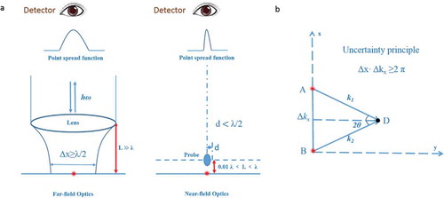
Based on the distance (L) between detected sample and probe, the propagation of electromagnetic field is categorized into three types [Citation3]: far-field (), near-field (
) and close-field (
), whose relevant theory is classical optics (wave optics or geometrical optics), near-field optics and quantum optics, respectively. The Abbe diffraction limit is applicable only in classical optics, while the spatial resolution in near-field optics is determined by the distance between probe and sample and the size of probes [Citation4]. In ), we show the imaging principle in far-field (objective lens) and near-field optics (nanometer-sized probe). Compared with far-field in which the point spread function of sample is decided by diffraction law, the spatial resolution in near-field optics is determined by the diameter of probe instead of incident wavelength when the probe-sample distance is smaller than the incident wavelength [Citation5]. The different spatial resolution in far-field and near-field optics can be easily explained by uncertainty principle [Citation5], as shown in ). Due to the conjugate relation, the position and wavevector of two luminous points (A and B) are described as follows:
Figure 1. Schematic of near-field optics. (a) The comparison between far-field and near-field optics. The point spread function in far-field optics is determined by diffraction limit, while the spatial resolution in near-field optics is determined by the size of probe. (b) The explanation of breaking the diffraction limit in near-field optics based on uncertainty principle.
where and
are the uncertainty of position and wavevector along the x direction, respectively.
and
represent the light from points A and B to the detector D, respectively.
is the angle between
and
. When the
is 90 degrees, the
reaches the maximum value of 2k, resulting in the Rayleigh criterion (
). However, the above conclusion is based on the prerequisite that
is always smaller than
, or in other words, any component of
is not a pure imaginary number. In the near-field optics, the electromagnetic field is localized among the sample surface, generating evanescent field, whose
is an imaginary number. According to
, we can obtain
larger than 2k and break the diffraction limit with
.
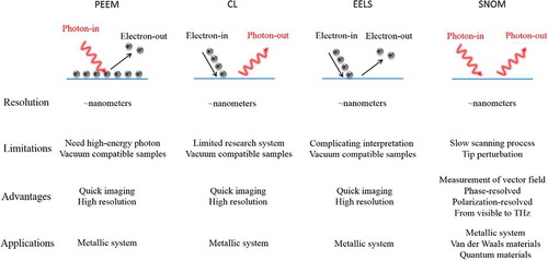
To study the physics in the near-field region, there are two schemes: electronic approach and near-field optical method. As shown in , a variety of techniques such as photon emission electron microscopy/low energy electron microscopy [Citation6–Citation8], cathode-luminescence (CL) spectroscopy [Citation9], electron energy loss spectroscopy (EELS) [Citation10–Citation13] and scanning near-field optical microscopy (SNOM) [Citation14–Citation17] enable the mapping of near-field information. Each of them has unique advantages and also is confronted with specific limitations. For example, the electronic approaches use the loss of electron energy (EELS) or induced CL to map the local density of optical states (LDOS). However, it is challenging to interpret the correlation between LDOS and other optical phenomena such as polaritonic eigenmodes. Meanwhile, the vacuum environment is necessary for all electron microscopy, which can only access the amplitude and neglect the important phase information. By the combination of near-field optics and scanning probe microscopy, the SNOM provides a promising way to access both near-field amplitude and phase and measure optical vector field with nanometer precision [Citation18–Citation22]. Although the point-by-point scanning is time-consuming and there is high demand on system stability, the SNOM has become a powerful method for near-field physics. Covering broad electromagnetic spectrum (from visible to terahertz [THz]), SNOM provides a lot of advantages, including nanoscale resolution (~10 nm), phase-resolved measurement [Citation23], polarization sensitivity [Citation24] and tip-enhanced effect [Citation25,Citation26]. Until now, the application of SNOM has expanded from metallic system to van der Waals (vdW) materials [Citation27], even quantum materials [Citation28,Citation29] and provided manifold novel and exciting insights into polaritonics, which have not been possible by standard far-field methods and other electronic approaches.
Figure 2. The comparison of four classical sub-wavelength approaches, including photon emission electron microscopy (PEEM), cathode-luminescence spectroscopy (CL), electron energy loss spectroscopy (EELS) and scanning near-field optical microscopy (SNOM).
In this paper, we review the up-to-date polaritonic studies on noble metals and vdW materials in the near-field region. We first give a brief overview on near-field optics, followed by its fundamental principle. Then, we summarize the up-to-date near-field polaritonic studies and related physics in three aspects: (1) In-situ electric field distribution around metallic nanostructures, (2) various polaritons in vdW materials, (3). quantum physical phenomena related to polaritonics in low-dimensional system. After that, we discuss the possibilities for combining scattering-type SNOM (s-SNOM) with other spectroscopic technique, transient measurement and THz technique. Finally, we give the nowadays challenges and present perspectives in the near-field optics.
2. Fundamental principle in near-field measurement
2.1. Precise control of tip position and background suppression
In this section, we give brief introduction about the two most important factors for near-field measurement, including precise control of tip–sample distance [Citation30,Citation31] and extraction of pure near-field signals [Citation32,Citation33]. Based on the principle of near-field optics, SNOM has to approach the tip to sample in the near-field range (~10 nm). The tip–sample distance (LT–S) need to keep stable during the scanning process. With self-feedback system, there are two methods for controlling LT–S: shear-force mode [Citation34] and tapping mode [Citation14]. In shear-force mode, the optical fiber tip is attached on the quartz tuning fork, vibrating parallel to the sample surface. The vibrating amplitude is strongly dependent on the shear-force between tip and sample. The linear increasing function between amplitude and LT–S provides an effective way to guarantee the tip in near-field region. The tapping mode is based on classical atomic force microscopy (AFM) technique, in which the tip vibrates perpendicular to the sample surface. The vibrating amplitude is highly sensitive to LT–S and provides a precise control of tip position. Compared with shear-force mode, the tapping mode is more widely used due to the ignorable damage to sample and simultaneously morphological and optical-imaging capability.
Another important process in near-field imaging is to extract the pure near-field signals from much larger far-field background. The SNOM is categorized into two types: aperture-SNOM [Citation35,Citation36] (a-SNOM) and s-SNOM [Citation37–Citation39], whose principle of background suppression is different. As shown in ), the incident laser is coupled into optical fiber for a-SNOM. In order to eliminate the far-field scattering background, the optical fiber with diameter (D) of just dozens of nanometers becomes a nano-light source and collector of localized optical signal. The spatial resolution of a-SNOM depends on the value of D, which also determines the transmission efficiency (η) of incident light. The efficiency becomes higher when the D is larger, i.e. η ~ 10−4 for D ~ 100 nm and η ~ 10−5 for D ~ 50 nm. Hence, we have to make a compromise between acceptable signal-to-noise ratio (large η) and high spatial resolution (small D). The best resolution of a-SNOM composed with optical fiber is ~50 nm. Although the spatial resolution can be further improved by combing metal nanowires (right panel, )), the application of a-SNOM is still restricted by the complicated fabrication of tip and light-leaking problem. Based on commercial AFM tip, s-SNOM, however, can achieve higher spatial resolution of ~1 nm. For s-SNOM, there are two schemes for focusing incident light onto the tip apex: indirect [Citation40,Citation41] (left panel, )) and direct [Citation19] (right panel, )). In indirect scheme, the far-field excitation of grating coupler on the tip shaft generates surface propagating plasmon (SPPs), adiabatically propagating through smooth tip surface and nanofocusing on the apex. The hotspot confined at tip apex provides intense nano-light source for locally probing optical properties of the sample. Similar with a-SNOM, this nanoscale focusing effectively eliminates the background from direct scattering from tip shaft and sample surface and, thus, makes analysis of experimental data simple and optical contrast easy to be understood. However, there are some limitations faced in the indirect-focusing scheme. First, the fabrication of linear-grates on AFM tip is complicated and the distance between gratings and the tip apex has to be optimized based on a trade-off between plasmonic propagation loss and background from the grating scattering. Second, the polarization and phase information of electric field is lost. Third, the poor coupling efficiency of plasmons (~0.1%) and small-field enhancement (~10) under tip apex limit the application of indirect scheme for probing polaritons in two-dimensional materials.
Figure 3. Experimental scheme of SNOM. (a) The illumination scheme of a-SNOM. (b) The illumination scheme of s-SNOM. (c) The scheme of oblique incidence-mode s-SNOM [Citation47]. (d) The scheme of transmission mode s-SNOM [Citation48]. (c) Reproduced with permission [Citation47]. Copyright 2002, Wiley-VCH. (d) Reproduced with permission [Citation48]. Copyright 2010, American Chemical Society.
![Figure 3. Experimental scheme of SNOM. (a) The illumination scheme of a-SNOM. (b) The illumination scheme of s-SNOM. (c) The scheme of oblique incidence-mode s-SNOM [Citation47]. (d) The scheme of transmission mode s-SNOM [Citation48]. (c) Reproduced with permission [Citation47]. Copyright 2002, Wiley-VCH. (d) Reproduced with permission [Citation48]. Copyright 2010, American Chemical Society.](/cms/asset/9074795f-3122-4946-acdd-bac1118f8715/tapx_a_1593051_f0003_oc.jpg)
In order to overcome these bottlenecks, Hillenbrand et al. [Citation42] directly focus light onto the tip-apex (right panel, )) and achieve strongly enhanced local field. In the direct-focusing scheme, it is difficult to extract the near-field signal from a big background noise caused by the scattering on the tip shaft and sample surface. The total scattered field (Etotal) from AFM tip can be expressed as , where the
and
represent useful near-field signal and background, respectively. The Etotal can be written in the form of a Fourier series:
where and
are the Fourier coefficient of
and
.
is the vibrating frequency of AFM tip. The detector output voltage (U) is proportional to light intensity (
), which is square of the electric field intensity (
). The expansion coefficients un can be expressed as [Citation42]
where is a proportionality constant related to the detector sensitivity. Given the approximation of
:
The noise arising from high-order background () is called additive noise (marked green). Because the vibrating tip causes a rapidly changing near-field interaction at higher harmonics (nΩ) while background is confined to direct current (dc) term and lower harmonics, the additive noise can be effectively eliminated by higher harmonic demodulation. Then,
Another noise caused by the interference between zero-order background () and near-field signal (
) is called multiplicative noise (marked red), which cannot be eliminated just by higher order harmonic demodulation method. Usually, we eliminate this multiplicative noise by adding a reference beam, named as ‘heterodyne’ [Citation43] or ‘pseudoheterodyne’ [Citation42] interferometric detection method. The suppression of background in these two methods is based on interference between near-field signal and reference wave with frequency shift (‘heterodyne’) or sinusoidal phase modulation (‘pseudoheterodyne’), respectively. In this review, we focus on ‘pseudoheterodyne’ method due to its advantages including easier operation, wide coverage of spectral range and higher signal-to-noise ratio. With reference beam, the total scattered field can be expressed as [Citation42]
The reference field can be written as
where and M are phase-modulation depth and frequency of reference beam, respectively. The phase offset (
) represents the averaged optical path difference between detected signal and reference wave. Based on Fourier expansion
where is the first kind Bessel function, mth order. The signal amplitude obtained by detector (
) is given by
The scattered signal harmonics with frequencies at split into sidebands with frequencies at
. Given that the multiplicative noise only exists at the frequency
but not at the sidebands
, we effectively avoid the zero-order background influence (K0) and eliminate the multiplicative background. Besides, we can simultaneously obtain pure near-field amplitude and phase from nth order. Substituting
and writing the complex coefficient
as
, we obtain:
The can be recovered from two sidebands
and
as
where , j and l are an even and odd integer, respectively. If we set j as 2 and l as 1, the
is equal to 2.63. Then, the nth harmonic amplitude Kn is
. The amplitude and phase of pure near-field signal can be expressed as [Citation42]
Although the background suppression and data interpretation are complicated, s-SNOM is widely used due to its unique advantages, including flexible options of commercial tip (metal or dielectric), phase- and polarization-resolved capability, nanoscale resolution and enhanced signal [Citation44–Citation46].
2.2. Experimental scheme
Based on the incident direction, we can categorize s-SNOM into two modes: oblique-incident mode [Citation47] ()) and transmission-mode [Citation48] ()). The s-SNOM is based on an AFM usually operating in the tapping mode. By Cassegrain objective or parabolic mirror, the incident laser is focused on the AFM tip and the scattered radiation is recorded simultaneously with topography. The combination of higher order harmonic demodulation (n ~ 3 or 4 in experiments) and pseudoheterodyne interferometric method mentioned above access both near-field amplitude and phase information. In order to exclude the error caused by man-kind operation, the measured near-field amplitude should be normalized by reference sample whose amplitude stays unchanged, usually as gold [Citation49] or silicon [Citation50]. The AFM tip provides in-plane momentum q ~ 1/φ [Citation51], where φ is the diameter of tip and compensates the momentum mismatch between polaritons and free-space photons.
For the transmission and oblique-incident modes, each of them has unique advantages and also specific limitations. In transmission mode, the sample is under homogenous illumination and the phase retardation can be neglected. However, the substrate should be transparent at incident frequency. In oblique-incidence mode, there is additional tip-enhanced effect, which is beneficial for launching polaritons. However, the phase retardation in oblique-incident mode is unavoidable. Hence, the transmission- and oblique-incidence mode are applied in different conditions, which are mapping of metal nanostructure with stronger near-field amplitude [Citation24,Citation52] and imaging of polaritons in vdW materials with weaker amplitude [Citation49,Citation50,Citation53], respectively.
2.3. Tip and incident polarization
There are two important parameters in the near-field optical measurement: tip material and polarization. Given the fact that s-SNOM is an invasive technique, we have to consider the perturbation from near-field interaction between tip and sample [Citation54]. Although metallic and dielectric tip can both compensate the momentum mismatch between polaritons and free-space light, the enhancement of local electric field and impact for optical imaging is quite different. The results [Citation54] in ) indicate that the electric field distribution of plasmonic nanostructures is sensitive to the near-field coupling between sample and tip. The classical dipolar mode of gold disk is observed by carbon nanotube (CNT) tip (left panel in )), while the metallic tip strongly disturbs the mode and gives an asymmetric pattern (right panel in )). The tip–sample coupling becomes a dominated factor when the polarizability of metallic tip is similar or even larger in strength than the dipole of gold disk. Hence, the metallic tip causes larger perturbation than dielectric tip. Another difference is stronger local field under metallic tip, compared with dielectric tip. In ), we show our simulated electric amplitude in the nanogap between tip and substrate with incident polarization parallel to the tip axis. Compared with silicon tip, the gold tip provides 10 times larger local field amplitude, which is important for launching of polaritons in low-dimensional materials. During the near-field scanning process, the metallic tip simultaneously plays the role of launcher and detector, while dielectric tip is just a detector. When we choose tip, we have to make a trade-off between small perturbation for the intrinsic near-field distribution (dielectric tip) and enhanced signal intensity (metallic tip). Usually, the dielectric and metallic tips are used for mapping the intrinsic near-field distribution of metal nanostructures and for studying polaritons in two-dimensional materials or spectroscopic information of the sample, respectively.
Figure 4. The influence of AFM tip in near-field measurement. (a) Topography and near-field amplitude of a gold nanodisk obtained by carbon nanotube (CNT) tip and Pt-coated Si tip [Citation54]. Scale bar, 100 nm. (b) The numerical simulation of local electric field between AFM tip and substrate. (a) Reproduced with permission [Citation54]. Copyright 2009, American Physical Society.
![Figure 4. The influence of AFM tip in near-field measurement. (a) Topography and near-field amplitude of a gold nanodisk obtained by carbon nanotube (CNT) tip and Pt-coated Si tip [Citation54]. Scale bar, 100 nm. (b) The numerical simulation of local electric field between AFM tip and substrate. (a) Reproduced with permission [Citation54]. Copyright 2009, American Physical Society.](/cms/asset/5200690d-88df-4528-aef1-97d12748a65f/tapx_a_1593051_f0004_oc.jpg)
Another important factor in near-field optics is the polarization, which is controlled by polarizers with S or P defined based on the plane formed by wavevector of light and the tip axis. The incident and detected polarization represent the polarizing state of incident light and light detected by the far-field detector. For the incident polarization, the and
have their specific advantages, which is stronger signal enhancement and small perturbation, respectively. The detected polarization (
or
) is critical for the correct interpretation of near-field maps, which is determined by the relationship between the local field components (Ex, Ey, Ez) and the signal detected at far-field detector [Citation16,Citation55]. The crossed-polarized detection configuration (
and
) is usually used to improve the signal-to-noise ratio and identify higher order modes of plasmonic antennas [Citation56]. With a simplified explanation, the selection of
and
is interpreted as a straightforward mapping of in-plane (Ex, Ey) and out-of-plane (Ez) components of local field [Citation57]:
where and
are the polarizability of tip along x and z direction, respectively. Following this assumption, the a-SNOM typically probes the transverse electric components (Ex, Ey), while the s-SNOM is sensitive to the vertical component (Ez) [Citation58,Citation59]. The above model is oversimplified to explain the sophisticated distribution in near-field measurements. Based on the reciprocity theorem, Neuman et al. [Citation57] indicated that
and
are determined by a more complicated weighted sum of the near-field components, including linear and quadratic functions. In their model, the detected signal can be expressed as
where is the incident field.
,
and
are the tip polarizability along x, y and z directions, respectively. The P-polarized detection scheme produces a signal proportional to a linear combination of the
and
, weighted by the polarizability tensor of the tip (
and
). However, the S-polarized detection scheme provides a signal with a quadratic combination of both in-plane (Ex, Ey) and out-of-plane (Ez) components, which is weighted by corresponding components of the tip polarizability tensor (
,
and
). Their model provides excellent insights in the interpretation of general near-field signal and quantitatively agrees well with experimental results.
3. Near-field distribution in metallic nanostructures
The resonant metallic antennas [Citation60] provide efficient conversion of free-space light into nanoscale-confined optical fields, which is important for various applications such as biosensors, surface-enhanced spectroscopy, energy transfer, etc. Because the interaction between antenna and detected molecules occurs in the near-field range, the interpretation of near-field distribution around antennas is the prerequisite to optimize antenna performance. Recently, s-SNOM shed new light on the understanding of both near-field amplitude and phase distribution in metal plasmonic [Citation20,Citation61–Citation64]. In this part, we review recent near-field studies on metal nanostructures, including single antenna, nanogapped antenna and different kinds of sophisticated antenna.
3.1. Single antenna
With resonant wavelength, the out-of-plane component of electric field (|Ez|) around linear metallic antennas behaves as a classical dipolar pattern, showing enhanced amplitude at the extremes and about π-reverse in the phase figure. As shown in ), the resonant wavelength of plasmonic dipole mode in gold nanorods can be tuned from mid-infrared (IR) range [Citation57] (MIR) to visible light [Citation65] (Vis) by changing the nanorods length. The near-field images simultaneously map the amplitude and phase around micrometer-sized and nanometer-sized antennas, showing classical dipolar patterns. In combination of near- and far-field measurement, Pablo et al. [Citation66] studied the spectral shift between the near- and far-field responses of linear gold antennas and revealed that the largest enhancement in surface enhanced IR spectrum is obtained when the near-field intensity, rather than far-field extinction, reaches its maximum. As shown in ), the spectral shift indicates that the maximum oscillation amplitude (detected as near-field signal) is at lower frequency compared with the maximum dissipation (detected by far-field spectrometer). This spectral shift is important for optimization of nano-antennas because the optical interaction between antenna and detected molecules occurs in near-field range, whereas the spectroscopic information is collected by far-field detector.
Figure 5. Near-field distribution around single metallic antennas in mid-infrared and visible range. (a) Near-field amplitude and phase of linear gold antenna with the incident wavelength at 11.06 μm [Citation57]. Scale bar, 1 μm. (b) Near-field amplitude and phase of gold nanorod structure with the incident wavelength at 632.8 nm [Citation65]. Scale bar, 100 nm. (c) Spectral shift between near- and far-field peak intensity of infrared gold antenna [Citation66]. (d) Near-field amplitude of gold triangle nanostructure with incident wavelength at 9.6 μm [Citation48]. Scale bar, 1 μm. (e) Near-field amplitude of silver nanoprisms with incident wavelength at 633 nm [Citation55]. Scale bar, 100 nm. (f) Near-field amplitude of gold nanodisks with incident wavelength at 875 nm [Citation56]. Scale bar, 200 nm. (g) Near-field amplitude of magnetic nickel nanodisks with incident wavelength at 633 nm [Citation67]. Scale bar, 100 nm. (a) Reproduced with permission [Citation57]. Copyright 2015, Wiley-VCH. (b) Reproduced with permission [Citation65]. Copyright 2014, American Chemical Society. (c) Reproduced with permission [Citation66]. Copyright 2013, American Physical Society. (d) Reproduced with permission [Citation48]. Copyright 2010, American Chemical Society. (e) Reproduced with permission [Citation55]. Copyright 2008, American Chemical Society. (f) Reproduced with permission [Citation56]. Copyright 2008, American Chemical Society. (g) Reproduced with permission [Citation67]. Copyright 2011, American Chemical Society.
![Figure 5. Near-field distribution around single metallic antennas in mid-infrared and visible range. (a) Near-field amplitude and phase of linear gold antenna with the incident wavelength at 11.06 μm [Citation57]. Scale bar, 1 μm. (b) Near-field amplitude and phase of gold nanorod structure with the incident wavelength at 632.8 nm [Citation65]. Scale bar, 100 nm. (c) Spectral shift between near- and far-field peak intensity of infrared gold antenna [Citation66]. (d) Near-field amplitude of gold triangle nanostructure with incident wavelength at 9.6 μm [Citation48]. Scale bar, 1 μm. (e) Near-field amplitude of silver nanoprisms with incident wavelength at 633 nm [Citation55]. Scale bar, 100 nm. (f) Near-field amplitude of gold nanodisks with incident wavelength at 875 nm [Citation56]. Scale bar, 200 nm. (g) Near-field amplitude of magnetic nickel nanodisks with incident wavelength at 633 nm [Citation67]. Scale bar, 100 nm. (a) Reproduced with permission [Citation57]. Copyright 2015, Wiley-VCH. (b) Reproduced with permission [Citation65]. Copyright 2014, American Chemical Society. (c) Reproduced with permission [Citation66]. Copyright 2013, American Physical Society. (d) Reproduced with permission [Citation48]. Copyright 2010, American Chemical Society. (e) Reproduced with permission [Citation55]. Copyright 2008, American Chemical Society. (f) Reproduced with permission [Citation56]. Copyright 2008, American Chemical Society. (g) Reproduced with permission [Citation67]. Copyright 2011, American Chemical Society.](/cms/asset/d66aa8c0-e1d3-4e65-99ab-fd61db9ef50a/tapx_a_1593051_f0005_oc.jpg)
Besides linear nanorods, there are other kinds of metal nanostructures with different plasmonic eigenmodes. Due to the strongly enhanced field at pointed ends and highly tunable plasmonic resonance, the prism structures serve as a key building block for nanoplasmonic applications. Schnell et al. [Citation48] and Rang et al. [Citation55] have revealed the near-field amplitude and phase in gold microprism ()) and silver nano-prism ()), respectively. In order to avoid the perturbation from AFM tip, they apply the silicon tip and S-polarized incident laser (). By controlling the detected polarizations (
or
), both in-plane (Ex) and out-of-plane (Ez) components of electric field is mapped. Furthermore, Esteban et al. [Citation56] ()) observe both fundamental dipole and higher order quadrupole resonance in gold nanodisks by using cross-polarization detection scheme (
and
) to reduce the background signal and the sample-tip coupling. By breaking the symmetry with oblique incidence, they observed the quadrupole composed with four amplitude lobes in gold disk with larger diameter, while the dipole in smaller disk displays two lobes of strong amplitude. Besides gold disk, Bonanni et al. [Citation67] ()) reported conventional dipole mode of localized magnetoplasmons in ferromagnetic nickel nanodisks. They also revealed the interaction between localized surface plasmons and magneto-optical activity, including polarizability and the signs of Kerr rotation.
3.2. Nanogapped antenna
Due to the strong enhancement of local electric field, the hotspot in nanogapped structure is quite important for the surface-enhanced spectroscopy [Citation68]. By using near-field imaging technique, we can directly visualize the spatial distribution of electric field in the nanogap and study the electromagnetic enhanced mechanism (EM) in enhanced spectroscopy. As shown in ), Pablo et al. [Citation69] observe the hotspot in the nanogap between two resonant gold rod structures. The near-field amplitude and phase reveal that the EM for elastic scattering in antenna-enhanced process is similar as the one in Raman scattering, whose enhancement factor is proportional to biquadrate of the ratio between local field and incident intensity. By combing s-SNOM with Raman spectrometer, Kusch et al. [Citation70] further realize in-situ mapping of near-field intensity distribution and enhanced inelastic Raman scattering in gold-dimer plasmonic structures. As shown in ), there is a direct correlation between surface-enhanced Raman spectroscopy hotspots and the electromagnetic near-field intensity. It is expected that we can synchronize the near-field imaging and Raman measurement to realize the simultaneous detection of near-field amplitude and Raman signal, which helps a lot for the studying of the growth mechanism of materials and chemical identification on nanoscale.
Figure 6. Near-field distribution in nanogapped metallic antennas. (a) Near-field amplitude and phase of resonant gapped gold-antenna with incident wavelength at 11.1 μm [Citation69]. Scale bar, 2 μm. (b) Electromagnetic hotspots in gold-dimer nanostructures and corresponding enhanced Raman spectrum [Citation70]. The incident wavelength is 633 nm. Scale bar, 200 nm. (c) Near-field image of infrared nanofocusing in tapered transmission lines [Citation71]. The incident wavelength is 9.3 μm. (d) Near-field amplitude and phase distribution around nanoscale gap in inverse bowtie gold antenna [Citation24]. (a) Reproduced with permission [Citation69]. Copyright 2012, Nature Publishing Group. (b) Reproduced with permission [Citation70]. Copyright 2017, American Chemical Society. (c) Reproduced with permission [Citation71]. Copyright 2011, Nature Publishing Group. (d) Reproduced with permission [Citation24]. Copyright 2010, American Chemical Society.
![Figure 6. Near-field distribution in nanogapped metallic antennas. (a) Near-field amplitude and phase of resonant gapped gold-antenna with incident wavelength at 11.1 μm [Citation69]. Scale bar, 2 μm. (b) Electromagnetic hotspots in gold-dimer nanostructures and corresponding enhanced Raman spectrum [Citation70]. The incident wavelength is 633 nm. Scale bar, 200 nm. (c) Near-field image of infrared nanofocusing in tapered transmission lines [Citation71]. The incident wavelength is 9.3 μm. (d) Near-field amplitude and phase distribution around nanoscale gap in inverse bowtie gold antenna [Citation24]. (a) Reproduced with permission [Citation69]. Copyright 2012, Nature Publishing Group. (b) Reproduced with permission [Citation70]. Copyright 2017, American Chemical Society. (c) Reproduced with permission [Citation71]. Copyright 2011, Nature Publishing Group. (d) Reproduced with permission [Citation24]. Copyright 2010, American Chemical Society.](/cms/asset/55ec9d5b-c6ea-4f39-bdc7-d0f12b1ffe20/tapx_a_1593051_f0006_oc.jpg)
Besides the nanodimer and double rod structure, Schnell et al. [Citation71] ()) realize the nanoscale focusing of IR electromagnetic field in tapered gold structure by introducing the classical antenna theory in radio frequency (RF) to nanophotonics. They conduct the near-field measurement of tapered transmission line, a classical concept in RF technology. The nano-IR images show high confinement factor (~200), defined by the ratio between incident (λ0) and plasmonic wavelength (λp), and strongly enhanced amplitude (~30) in the nanogap. Furthermore, Schnell et al. [Citation24] ()) also reconstruct the vectorial near-field distribution (both in-plane and out-of-plane component) and the polarization state in the nanogapped inverse bowtie structures. The detected signal is expressed as followings: , where
,
,
are the near-field amplitude and phase of the x and z components in the bowtie structure.
and
are the diagonal tensor of elongate tip. The
is the polarizer angles before the detector. By analyzing the variation trend of near-field amplitude and phase with changing
, they, for the first time, experimentally obtain the diagonal tensor of elongate AFM tip, as
~ 2
.
3.3. Sophisticated antennas
The applications of plasmonic antennas rely on the near-field interaction between the antenna and its load, a concept adopted from RF technology. Schnell et al. [Citation72] indicate that local near-field amplitude and phase of IR antenna are sensitive to the antenna load, which can be effectively tuned by metal bridges. As shown in ), the z-component of the electric field distribution (Ez) in near-field images displays a clear transition from single dipolar-like pattern for continuous nanorod to twin dipolar-like patterns for fully cut nanorod, when the gapped antenna is progressively loaded (decreasing width of metal bridge). This transition agrees well with classical circuit theory in the RF range, predicting a transition from inductive to capacitive load impedance. Another important concept in plasmonic is Fano interference, whose interpretation is usually based on far-field spectroscopy and calculated distribution of charge density before the development of near-field optics. The far-field characterization of complicated Fano interference in multi-resonant metamolecules is insufficient and ambiguous because that the same far-field scattering behavior can be caused by different near-field distributions. Pablo et al. [Citation73] unravel the interference between ‘dark mode’ and ‘bright mode’ for Fano resonances in heptamer gold structures. This is the first near-field imaging of interference between electromagnetic eigenmodes in plasmonic metamolecules. As shown in ), they give both near-field amplitude and phase distribution of heptamer plasmonic antennas. In combination of calculated far-field extinction spectrum and near-field imaging, they also build the connection between the near-field and far-field optical response. Another important antenna is Archimedean spiral antennas, with capability to realize nanofocusing of circularly polarized IR light, such as left circularly polarized (LCP) and right circularly polarized (RCP) light. As shown in ), the real-space image of Archimedean spiral antennas [Citation52] shows different react to LCP and RCP, which is strong and weak amplitude in the antenna center, respectively. The experimental results indicate that there is a close connection between IR chiral nanoantennas and classical antenna theory in RF and the near-field distribution can be explained by traveling and standing waves, which are usual concepts in RF. In ), Bernhard et al. [Citation74] give the near-field amplitude and phase in V-shaped antennas, which is another widely used antenna for designing phased array metasurfaces. By using ‘far-field transformation’, their near-field images can predict the corresponding far-field behavior of optical structures and give implications for their applications.
Figure 7. Near-field distribution of sophisticated metallic antennas. (a) Near-field images of progressively loaded nanoantennas [Citation72], including continuous rod, thick metal-bridge rod, tiny metal-bridge rod and fully cut rod. The length of gold rods is 1550 nm and the incident wavelength is 9.6 μm. (b) Near-field amplitude and phase of Fano interference in symmetric heptamer structures composed by seven gold nanodisks at a wavelength of 9.3 μm [Citation73]. (c) Near-field distribution around Archimedean spiral antennas illuminated by left (LCP) and right (RCP) circularly polarized light [Citation52]. The incident wavelength is 9.3 μm. (d) Near-field intensity and phase maps of V-shaped antennas for different sizes [Citation74]. The nano-infrared images demonstrate near-field phase varies as a function of antenna size. (a) Reproduced with permission [Citation72]. Copyright 2009, Nature Publishing Group. (b) Reproduced with permission [Citation73]. Copyright 2011, American Chemical Society. (c) Reproduced with permission [Citation52]. Copyright 2015, American Chemical Society. (d) Reproduced with permission [Citation74]. Copyright 2015, American Chemical Society.
![Figure 7. Near-field distribution of sophisticated metallic antennas. (a) Near-field images of progressively loaded nanoantennas [Citation72], including continuous rod, thick metal-bridge rod, tiny metal-bridge rod and fully cut rod. The length of gold rods is 1550 nm and the incident wavelength is 9.6 μm. (b) Near-field amplitude and phase of Fano interference in symmetric heptamer structures composed by seven gold nanodisks at a wavelength of 9.3 μm [Citation73]. (c) Near-field distribution around Archimedean spiral antennas illuminated by left (LCP) and right (RCP) circularly polarized light [Citation52]. The incident wavelength is 9.3 μm. (d) Near-field intensity and phase maps of V-shaped antennas for different sizes [Citation74]. The nano-infrared images demonstrate near-field phase varies as a function of antenna size. (a) Reproduced with permission [Citation72]. Copyright 2009, Nature Publishing Group. (b) Reproduced with permission [Citation73]. Copyright 2011, American Chemical Society. (c) Reproduced with permission [Citation52]. Copyright 2015, American Chemical Society. (d) Reproduced with permission [Citation74]. Copyright 2015, American Chemical Society.](/cms/asset/4cf3d896-0500-41c3-a317-cedb18f4bcfb/tapx_a_1593051_f0007_oc.jpg)
4. Near-field optics in vdW materials
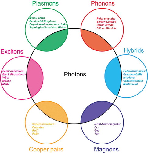
Polaritons [Citation27,Citation29], coupling photons with other quasiparticles such as plasmons, phonons and excitons, etc., pave the way for realizing ultimate targets in nanophotonics, such as confining light to nanoscale, enhancing light-matter interaction and manipulating uncharged photons. Besides the thoroughly studied plasmon polaritons in noble metal system [Citation75,Citation76], there are many other varieties of polaritons observed in vdW materials (), including those formed by plasmons in semimetal [Citation77], phonons in polar crystal [Citation49], excitons in semiconductors [Citation78], cooper pairs in superconductors [Citation29], magnons in ferromagnets [Citation29] and hybrids in heterostructures [Citation79–Citation81]. Compared with noble metals, atomically flat vdW materials support polaritonic modes with higher confinement and super tunability. The operating frequencies of polaritons in vdW materials span from ultraviolet to microwave spectral range, covering almost the entire electromagnetic spectrum. Recently, state-of-the-art near-field technique has realized real-space imaging of polaritonic waves in vdW materials and unprecedented regulating of polaritonic response at the single atomic planes. The nano-imaging and nano-spectroscopic measurements of polaritons have provided abundant insights into quantum phenomena that happened in their host materials and novel dispersion relations of condensed-matter excitation, which is inaccessible by conventional far-field optics. Until now, s-SNOM is the only approach to map the amplitude and phase of polaritons in vdW materials. In this section, we review recent near-field studies on polaritons in vdW materials, mainly focusing on plasmon polaritons in graphene, hyperbolic phonon polaritons (HPPs) in boron nitride, exciton polaritons (EPs) in semiconductors and polaritons in heterostructures.
Figure 8. Polaritons in low-dimensional materials. Polaritons are collective excitation from coupling photons with other quasiparticles, such as plasmons in electron-rich systems, infrared-active phonons in polar insulators, excitons in semiconductors, cooper-pairs in superconductors, spin resonances in (anti)-ferromagnets and hybrids in heterostructures.
4.1. Plasmon polaritons in graphene
Graphene is the first generation of vdW materials [Citation82,Citation83] and its plasmonic response is thoroughly studied because of the unique linear energy dispersion and universal optical conductivity (the constant conductivity over a broad range of frequencies: ) [Citation84,Citation85]. Due to its highly tunable Drude weight and high mobility of charge carriers, graphene provides state-of-the-art plasmonics with unique properties including gate-tunable dispersion, ultrahigh confinement (λ0/λp ~ 50), broadband resonance (MIR to THz) and extra-sensitivity to external environment. Recently, several near-field experiments have visualized the propagating or localized plasmon polaritons in monolayer or bilayer graphene ( and ), manipulated the plasmonic scattering behavior () and explored the applications ().
Figure 9. Surface plasmon polaritons in monolayer graphene. (a) Near-field spectroscopic measurement and theoretically calculated dispersion of Dirac plasmons in monolayer graphene [Citation51]. (b) s-SNOM scheme (upper), experimental amplitude of graphene plasmons (middle) and calculated local density of optical states (bottom) [Citation53]. The incident wavelength is 9.7 μm. (c) Nano-image of graphene plasmons launched by gold antenna under liquid-nitrogen temperature. The incident wavelength is 11.28 μm [Citation88]. (d) Plasmonic hotspots inside graphene nanobubbles on boron nitride substrate [Citation89]. The incident frequency is 910 cm−1. (e) Asymmetric plasmonic fringes induced by superposition of propagating and localized modes in graphene nanoribbons [Citation90]. The incident frequency is 1184 cm−1. (f) Experimental (left) and calculated (right) near-field amplitude of graphene rectangle resonators, representing 1D edge mode and 2D sheet mode [Citation93]. The incident wavelength is 11.31 μm. (g) Edge plasmons at the top boundary of graphene nanoribbons [Citation92]. The incident frequency is 1160 cm−1. Scale bars in all panels represent 200 nm, except for 1 μm in (c). (a) Reproduced with permission [Citation51]. Copyright 2011, American Chemical Society. (b) Reproduced with permission [Citation53]. Copyright 2012, Nature Publishing Group. (c) Reproduced with permission [Citation88]. Copyright 2018, Nature Publishing Group. (d) Reproduced with permission [Citation89]. Copyright 2016, American Chemical Society. (e) Reproduced with permission [Citation90]. Copyright 2017, American Chemical Society. (f) Reproduced with permission [Citation93]. Copyright 2016, Nature Publishing Group. (f) Reproduced with permission [Citation92]. Copyright 2015, American Chemical Society.
![Figure 9. Surface plasmon polaritons in monolayer graphene. (a) Near-field spectroscopic measurement and theoretically calculated dispersion of Dirac plasmons in monolayer graphene [Citation51]. (b) s-SNOM scheme (upper), experimental amplitude of graphene plasmons (middle) and calculated local density of optical states (bottom) [Citation53]. The incident wavelength is 9.7 μm. (c) Nano-image of graphene plasmons launched by gold antenna under liquid-nitrogen temperature. The incident wavelength is 11.28 μm [Citation88]. (d) Plasmonic hotspots inside graphene nanobubbles on boron nitride substrate [Citation89]. The incident frequency is 910 cm−1. (e) Asymmetric plasmonic fringes induced by superposition of propagating and localized modes in graphene nanoribbons [Citation90]. The incident frequency is 1184 cm−1. (f) Experimental (left) and calculated (right) near-field amplitude of graphene rectangle resonators, representing 1D edge mode and 2D sheet mode [Citation93]. The incident wavelength is 11.31 μm. (g) Edge plasmons at the top boundary of graphene nanoribbons [Citation92]. The incident frequency is 1160 cm−1. Scale bars in all panels represent 200 nm, except for 1 μm in (c). (a) Reproduced with permission [Citation51]. Copyright 2011, American Chemical Society. (b) Reproduced with permission [Citation53]. Copyright 2012, Nature Publishing Group. (c) Reproduced with permission [Citation88]. Copyright 2018, Nature Publishing Group. (d) Reproduced with permission [Citation89]. Copyright 2016, American Chemical Society. (e) Reproduced with permission [Citation90]. Copyright 2017, American Chemical Society. (f) Reproduced with permission [Citation93]. Copyright 2016, Nature Publishing Group. (f) Reproduced with permission [Citation92]. Copyright 2015, American Chemical Society.](/cms/asset/3eac6b24-69ca-436b-8528-05e52ed52e54/tapx_a_1593051_f0009_oc.jpg)
Figure 10. Plasmon polaritons in bilayer graphene. (a) Left panel: experimental measurement of voltage-dependent plasmonic wavelength in monolayer (SLG) and bilayer (BLG) graphene. Right panel: theoretical calculation of voltage- and frequency-dependent imaginary part of the optical conductivity. The double-headed arrows indicate plasmon-off region of bilayer graphene [Citation95]. (b) Near-field study of interaction between plasmons and intrinsic phonons in highly doped double-layer (left) and bilayer graphene (right) [Citation94]. The dispersed symbols represent experimental data and background color indicates the imaginary part of the calculated Fresnel reflection coefficient. Inset: representative near-field images of graphene plasmons and corresponding symmetry of phonon-induced charge densities. (a) Reproduced with permission [Citation95]. Copyright 2015, American Chemical Society. (b) Reproduced with permission [Citation94]. Copyright 2017, American Chemical Society.
![Figure 10. Plasmon polaritons in bilayer graphene. (a) Left panel: experimental measurement of voltage-dependent plasmonic wavelength in monolayer (SLG) and bilayer (BLG) graphene. Right panel: theoretical calculation of voltage- and frequency-dependent imaginary part of the optical conductivity. The double-headed arrows indicate plasmon-off region of bilayer graphene [Citation95]. (b) Near-field study of interaction between plasmons and intrinsic phonons in highly doped double-layer (left) and bilayer graphene (right) [Citation94]. The dispersed symbols represent experimental data and background color indicates the imaginary part of the calculated Fresnel reflection coefficient. Inset: representative near-field images of graphene plasmons and corresponding symmetry of phonon-induced charge densities. (a) Reproduced with permission [Citation95]. Copyright 2015, American Chemical Society. (b) Reproduced with permission [Citation94]. Copyright 2017, American Chemical Society.](/cms/asset/5ca49ccb-b874-4ba4-9d6d-bfa74f447b2f/tapx_a_1593051_f0010_oc.jpg)
Figure 11. Nano-reflectors for graphene plasmons. (a) Totally reflected plasmons at graphene edges [Citation50]. The incident frequency is 892 cm−1. (b) Calculated reflectance of graphene plasmons at a sharp Gaussian-shaped wrinkle as a function of wrinkle half-width w, for different wrinkle heights, h [Citation97]. The P1, P2, P3 indicate large transmission, total reflection and total transmission, respectively. The incident wavelength is 10 μm. c) Experimental (dispersed symbols) and theoretical (solid lines) plasmonic reflectance as a function of the height of nano-step [Citation98]. Red and black solid lines represent disconnected and continuous graphene at the step, respectively. (d) Plasmonic reflection at graphene grain boundaries [Citation99]. The experimental (black squares) and modeled (red curve) twin fringe profiles are extracted from near-field images with the incident wavelength at 11.3 μm, as shown in inset. (e) Man-made tunable carbon nanotube (CNT) reflectors for graphene plasmons [Citation100]. Upper panel: Schematic of CNT-reflector. Bottom panel: the experimental (blue line) and theoretical (gray line) near-field amplitude along the line perpendicular to the CNT with gate-voltage of −2 V. (f) Plasmonic reflectance at domain walls in bilayer graphene [Citation101]. Left panel: plasmonic interference patterns around the domain walls (black arrow). Right panel: the experimentally extracted plasmonic reflectance at the domain walls in bilayer graphene. (a) Reproduced with permission [Citation50]. Copyright 2012, Nature Publishing Group. (b) Reproduced with permission [Citation97]. Copyright 2017, American Chemical Society. (c) Reproduced with permission [Citation98]. Copyright 2013, American Chemical Society. (d) Reproduced with permission [Citation99]. Copyright 2013, Nature Publishing Group. (e) Reproduced with permission [Citation100]. Copyright 2016, American Physical Society. (f) Reproduced with permission [Citation101]. Copyright 2017, American Chemical Society.
![Figure 11. Nano-reflectors for graphene plasmons. (a) Totally reflected plasmons at graphene edges [Citation50]. The incident frequency is 892 cm−1. (b) Calculated reflectance of graphene plasmons at a sharp Gaussian-shaped wrinkle as a function of wrinkle half-width w, for different wrinkle heights, h [Citation97]. The P1, P2, P3 indicate large transmission, total reflection and total transmission, respectively. The incident wavelength is 10 μm. c) Experimental (dispersed symbols) and theoretical (solid lines) plasmonic reflectance as a function of the height of nano-step [Citation98]. Red and black solid lines represent disconnected and continuous graphene at the step, respectively. (d) Plasmonic reflection at graphene grain boundaries [Citation99]. The experimental (black squares) and modeled (red curve) twin fringe profiles are extracted from near-field images with the incident wavelength at 11.3 μm, as shown in inset. (e) Man-made tunable carbon nanotube (CNT) reflectors for graphene plasmons [Citation100]. Upper panel: Schematic of CNT-reflector. Bottom panel: the experimental (blue line) and theoretical (gray line) near-field amplitude along the line perpendicular to the CNT with gate-voltage of −2 V. (f) Plasmonic reflectance at domain walls in bilayer graphene [Citation101]. Left panel: plasmonic interference patterns around the domain walls (black arrow). Right panel: the experimentally extracted plasmonic reflectance at the domain walls in bilayer graphene. (a) Reproduced with permission [Citation50]. Copyright 2012, Nature Publishing Group. (b) Reproduced with permission [Citation97]. Copyright 2017, American Chemical Society. (c) Reproduced with permission [Citation98]. Copyright 2013, American Chemical Society. (d) Reproduced with permission [Citation99]. Copyright 2013, Nature Publishing Group. (e) Reproduced with permission [Citation100]. Copyright 2016, American Physical Society. (f) Reproduced with permission [Citation101]. Copyright 2017, American Chemical Society.](/cms/asset/3417e722-cc66-4a49-be6a-87ecbaf8c751/tapx_a_1593051_f0011_oc.jpg)
Figure 12. The applications of graphene plasmons. (a) Phase control of infrared light by gate-tunable graphene plasmons [Citation103]. Upper panel: schematic of experimental configuration. Bottom panel: theoretical (solid lines) and experimental (dispersed circles) phase shift, which can be changed from 0 to 2π. (b) Hybridized polaritons in graphene/hBN heterostructures [Citation104]. Upper panel: with monolayer graphene, both amplitude and wavelength of phonon polaritons in pristine hBN increase. Bottom panel: the gate-tunable hyperbolic phonon–plasmon polaritons (HP3) in graphene/hBN and un-tunable hyperbolic phonon polaritons (HP2) in hBN. The incident frequency is 1495 cm−1. Scale bar, 300 nm. (a) Reproduced with permission [Citation103]. Copyright 2017, Nature Publishing Group. (b) Reproduced with permission [Citation104]. Copyright 2015, Nature Publishing Group.
![Figure 12. The applications of graphene plasmons. (a) Phase control of infrared light by gate-tunable graphene plasmons [Citation103]. Upper panel: schematic of experimental configuration. Bottom panel: theoretical (solid lines) and experimental (dispersed circles) phase shift, which can be changed from 0 to 2π. (b) Hybridized polaritons in graphene/hBN heterostructures [Citation104]. Upper panel: with monolayer graphene, both amplitude and wavelength of phonon polaritons in pristine hBN increase. Bottom panel: the gate-tunable hyperbolic phonon–plasmon polaritons (HP3) in graphene/hBN and un-tunable hyperbolic phonon polaritons (HP2) in hBN. The incident frequency is 1495 cm−1. Scale bar, 300 nm. (a) Reproduced with permission [Citation103]. Copyright 2017, Nature Publishing Group. (b) Reproduced with permission [Citation104]. Copyright 2015, Nature Publishing Group.](/cms/asset/873cc0d2-e441-4869-858f-cf506aa72a7b/tapx_a_1593051_f0012_oc.jpg)
4.1.1. Plasmons in monolayer graphene
Given that there is a large momentum mismatch between graphene plasmons () and free-space photons (
), it is necessary to provide enough momentum compensation, which is realized through metal grating structure or periodic nanoribbon arrays [Citation86,Citation87] in the far-field measurement and metallic AFM tip in the near-field measurement [Citation51]. displays the near-field imaging of graphene plasmons with different modes, including two-dimensional sheet mode (propagating or localized), one-dimensional edge mode and waveguide mode. As shown in ), Fei et al. [Citation51] give the near-field spectroscopic information of Dirac plasmon in graphene and its interaction with surface phonon of the SiO2 substrate using their high momentum spectroscopy and nano-imaging technique. The experimental results demonstrate that the AFM tip can provide enough momentum compensation to excite graphene plasmon and SiO2 phonon mode. The enhanced and blue-shifted near-field amplitude at graphene/SiO2 interface is induced by strong plasmon–phonon interaction between graphene and SiO2 substrate. They also calculate the complex reflection coefficient (rp) as a function of plasmonic wavevector (q) and incident frequency (ω). The theoretical calculation (right panel, )) clearly shows the interaction and hybridization between graphene plasmon and optical phonon of SiO2 substrate. After that, two research groups [Citation50,Citation53] independently realize the nanoscale real-space imaging of propagating and localized graphene plasmons on different substrates (SiC or SiO2). The tip-launched plasmons propagate radially, reflect back upon reaching the graphene edge and finally form interference standing waves, showing fringes with spacing of half the plasmonic wavelength. The near-field amplitude of a tapered graphene ribbon ()) agrees well with the calculated LDOS. The experiments confirm the strong optical field confinement (λ0/λp ~ 40) and in-situ gate-tunable properties of graphene plasmons. Although graphene plasmons provide a platform for active manipulation of photons at the nanoscale, plasmonic dissipation in graphene is substantial at room temperature. Recently, Ni et al. [Citation88] have determined the fundamental limits to graphene plasmonics with their homemade cryogenic s-SNOM. Under liquid-nitrogen temperature (~60 K), they effectively avoid the intervalley scattering and electron–electron scattering in graphene and reduce the plasmonic damping. As shown in ), the longest lifetime of graphene plasmons can reach up to ~1.6 ps, which is an order of magnitude larger than the value in room temperature (~0.1 ps).
Compared with propagating mode on semi-infinite flake, the plasmonic hotspots in confined graphene nanostructures [Citation89–Citation91], such as nanobubble, nanoribbon and nanostripe, provide higher spatial confinement and stronger field enhancement. As shown in ), Fei et al. [Citation89] observe the hotspots in graphene nanobubbles, showing strong potential for plasmon-enhanced infrared spectrum of biomolecules in aqueous environment. The hotspots in nanobubbles generate higher spatial confinement factor (Vhotspot/ ~ 106) and stronger amplitude (~twice) compared with propagating mode. Furthermore, Fei et al. [Citation90] identify two different modes of surface plasmons in graphene nanoribbons. As shown in ), a mixed surface propagating plasmon (SPP) and surface plasmon resonance (SPR) mode is excited when the in-plane component of the incident field (Ein) is perpendicular to the nanoribbons, while the pure SPP mode is excited if Ein is parallel to the nanoribbon. Combining the near-field measurements and numerical simulation, they indicate that the asymmetric fringes (right panel, )) in perpendicular condition are caused by the superposition of tip-launched SPP mode and tip-enhanced SPR mode.
Given that Drude weight is reduced at edges where the free charge carriers only exist ‘on one side’, one-dimensional edge modes of graphene plasmon display much weaker intensity and smaller wavelength compared with two-dimensional sheet modes. Because that the reflectors, such as sharp corners or small defects, are necessary for the observation of these edge modes, their real-space images usually exist in lithography-patterned graphene nanostructure rather than the mechanically exfoliated graphene flakes with natural, smooth edges. As shown in , two research groups [Citation92,Citation93] observe both fundamental and higher order edge modes. The edge modes of graphene plasmons manifest as black dots caused by Fabry–Perot resonance between tip-launching and corner-reflecting edge plasmons. The edge modes exhibit strong confinement of electromagnetic field (λ0/60), generating the ultrahigh volume confinement of 10−8. With the combination of numerical simulations and near-field measurements, Nikitin A et al. [Citation93] disentangle various Fabry–Perot modes (both fundamental and higher order) in graphene resonator, including edge mode, sheet mode and even wave-guiding mode. Their results indicate that the metallic AFM tip acts as a dipole excitation source and has a position-dependent influence on the plasmonic modes, which challenges the interpretation of observed patterns without numerical simulation.
4.1.2. Plasmons in bilayer graphene
There are two kinds of interaction between two graphene layers: strong coupling in Bernal-stacking bilayer and weak coupling in randomly stacking double layer [Citation94]. Compared with monolayer prototype, the bilayer graphene shows smaller plasmonic wavelength, while double layer shows larger one. Besides, the Bernal-stacking bilayer graphene exhibits large plasmon-off region due to the strong electron quantum tunneling effect. As shown in ), Fei et al. [Citation95] realize the turnoff of plasmons in bilayer graphene, which is important for transistors and optical switches in plasmonic circuits. There is an extended gate voltage range without any detectable plasmons in bilayer graphene (double-headed arrows in )). The plasmonic turnoff region in bilayer graphene can reach up to ~50 V at the incident frequency of 883 cm−1.
Another near-field measurement [Citation94] demonstrates that the intrinsic phonon-induced dipole in random stacking monolayers and Bernal-stacking bilayer is different ()). In random stacking condition (left panel, )), inversion symmetry (insets in )) cancels the induced-charge contribution and gives Raman-active optical phonon at 1580 cm−1. By breaking the inversion symmetry, the bilayer graphene (right panel, )) generates IR active optical phonon at 1580 cm−1. In the highly doped graphene, both experiment and theoretical calculation show different plasmonic dispersions in stacking monolayers and bilayer. We can clearly observe an anticrossing behavior at the intrinsic optical phonon frequency in the bilayer, whereas this feature is missing on monolayers. The nano-IR images (insets in )) show that the interaction between plasmon and IR-active optical phonon has a large influence on the plasmonic lifetime.
4.1.3. Scattering of graphene plasmons
It is important to study the plasmonic scattering behavior for analyzing and controlling graphene plasmons. For graphene plasmon, there are two types of reflectors [Citation96]: topographic corrugations including physical edge, wrinkle, bubble and nano-step; and electronic boundaries including grain boundary, gated CNT and domain wall. In , we give the review of different reflectors for graphene plasmon with controllable reflection coefficient (r) from nearly zero (total transmission) to one (total reflection).
The physical edges are first observed reflector for graphene plasmon with r ~ 1 and phase shift of about −0.8π. As shown in ), the tip-launched plasmon propagates radially, reflects upon reaching the edges and finally forms interference standing wave, showing periodic fringes parallel to the edge [Citation50]. Another important topographic reflector is corrugations, categorized into two types: smooth one () and sharp one (h ≥ ω), where h and ω are the height and full width of corrugation, respectively. For smooth case, the dominated factor of reflection is a topographic effect and the plasmonic scattering is largely adiabatic. Combining the analytical calculation and numerical simulation, Nikitin A et al. [Citation97] give the position and maximum value of reflectance as follows:
where Rmax is the maximum value of reflectance (),
is the spectral position of the Rmax,
and
represent the dielectric permittivities of superstrate and substrate around the graphene, respectively. For sharp corrugation, the condition is quite complicated because the localized cavity mode may be excited. As shown in ), the reflectance can be effectively tuned from zero to one by changing the topographic parameters of corrugation. The sharp corrugation provides us a perfect reflector (P2 in )) or transmitter (P3 in )) for graphene plasmons. Unfortunately, the physical mechanism behind this broadly tunable reflector is still ambiguous, and the graphene absorption is neglected in the calculation. In ), Chen et al. [Citation98] show that an ultra-narrow step of only a few nanometers, which is two orders of magnitude smaller than plasmonic wavelength, also provides an effective reflector, with rmax ~0.6 at 5 nm height. The r is strongly dependent on the height of nanostep and can be tuned from near zero to 0.6. Their experiments indicate that discontinuous graphene shows larger r compared with continuous graphene for all step heights. The numerical simulation has identified the key factor for the plasmonic reflection as electrical connectivity of graphene at the step, rather than just geometrical effect.
Besides geometrical protuberance, electronic boundaries also induce the plasmonic scattering. The anomalous reflection of graphene plasmons has been observed at various electronic boundaries with width of just a few nanometers. The plasmonic reflection at electronic boundary is coming from two mechanisms: one is local fluctuations in plasmonic wavelength caused by electronic heterogeneity and the other is changed optical conductivity of graphene caused by bound states. In ), Fei et al. [Citation99] show that the atomic-length scale grain boundaries in graphene, which are invisible in AFM measurement, provide an effectively plasmonic reflector (R ~ 0.08) and controllable phase shift (−0.6π < Δφ < −1.6π). Given that the grain boundary is easily absorbed by molecules in ambient environment, there is high concentration of charge carriers located at boundaries, resulting in the enhancement of plasmonic wavelength and damping rate. The grain boundaries also effectively reduce the optical conductivity of graphene. The combination of these two reasons causes the plasmonic scattering. Another man-made electronic boundary is gated CNTs fabricated by Jiang et al. [Citation100], as shown in ). Their near-field measurements and theoretical calculation indicate that the mechanism of man-made reflector is the enhanced optical conductivity caused by optical transition involving these bound states related to gated-CNTs. The r can be tuned by the chemical potential of graphene, and the maximum value reach up to ~0.5. In bilayer graphene ()), there is another plasmonic reflector called domain walls [Citation101], which are separating channel of AB and BA stacking regions. The local conductivity tensor and corresponding electrodynamic impedance can be significantly changed by topological and conducting one-dimensional channels at domain walls. Hence, the interaction between topologically protected chiral mode and plasmon generates tunable reflectance (0 < R < 0.3) and phase retardation (−0.6π < Δφ < −1.6π), which are sensitive to the types of domain walls (tensile or shear) [Citation102], chemical potential and potential bias between graphene layers.
4.1.4. Applications of graphene plasmons
The application of graphene plasmons is mainly based on the gate-tunable Drude weight and strong interaction with other polaritons or photons. As shown in ), the near-field measurement [Citation103] indicates that gated-graphene heterostructures provide a plasmonic modulator with high efficiency (Vπ ~ 2.5 V, where Vπ is the voltage needed to realize π-phase shift) and small footprint (~350 nm). By spatially controlling the plasmonic phase velocity and wavelength, Achim et al. first realize the continuously tunable phase shift (0 < φ < 2π) of plasmon and the corresponding outcoming photons in a nanoscale phase modulator. This work opens the door of two-dimensional transformation optics. Another important experiment [Citation104] is to control the properties of polaritons in vdW materials based on gate-tunable graphene plasmons. With the help of strong coupling between graphene plasmons and other polaritons in vdW materials, we can realize graphene-induced tunability via electrostatic gating method. As shown in ), the formation of hybridized phonon–plasmon polaritons (HPPPs) in graphene/hexagonal boron nitride (hBN) heterostructure enables ~50% increase of both amplitude and wavelength of phonon polaritons in hBN, which is difficult to realize electrostatic gating due to the insulating properties of hBN crystal. Based on graphene, the polaritonic wavelength can be effectively tuned in a broad range. The graphene-induce tunability is expected to be generic for many vdW materials and helpful for nanoscale manipulation of polaritons.
4.2. Phonon polaritons in vdW materials
Due to the constant dielectric tensor, the isofrequency surface of propagating wave in isotropic materials is a sphere. Differently, the hyperbolic materials possess in-plane () and out-of-plane (
) component of dielectric tensor with opposite signs, as
. As shown in ), the dispersion in hyperbolic materials is two types of hyperboloids [Citation105], in which the magnitude of polaritonic wavevector (kp) is unlimited but its propagation is directional. The hyperbolic waves is first observed in man-made meta-materials, or called hyperbolic meta-materials (HMMs) [Citation106–Citation109], which is important in super-resolution imaging [Citation106], enhanced spontaneous radiation [Citation110] and negative refraction [Citation111,Citation112]. However, the spatial resolution and optical confinement in HMMs are strongly restricted due to the limited size of the artificial unit cell in micro-nano fabrication. The high loss associated with the constituent noble metals and the complicated fabrication also limit the application of HMMs. Recently, the near-field experimental results [Citation49] have identified the hBN as a natural hyperbolic material in the technologically important IR range and realized the real-space imaging of HPPs with large momentum. Compared with its graphene plasmon counterpart, the HPPs possess unique properties including high-quality factor, highly directional propagation and ultraslow group velocity.
Figure 13. Hyperbolic phonon polaritons (HPPs) in boron nitride. (a) Hyperbolic behavior of natural hBN crystal, which gives two separate spectral bands called lower and upper Reststrahlen bands with opposite-signed in-plane () and out-of-plane (
) dielectric permittivity [Citation105]. The corresponding hyperboloid-type dispersion of polaritons is shown in left (type 1) and right (type 2) panels. (b) Nano-infrared images of HPPs in a tapered hBN crystal [Citation49]. The incident frequency is 1550 cm−1. Scale bar, 800 nm. c) In-plane hyperbolic phonon polaritons in nano-patterning boron nitride crystal [Citation113]. Left panel: near-field image of concave wavefront of phonon polaritons in boron nitride metasurfaces. Right panel: schematic of the experiment. (d) Volume-confined polaritons (M0) and surface polaritons (SM0) near the edge of hBN crystal [Citation114]. The incident frequency is 1420 cm−1. Scale bar, 2 μm. e) Manipulation of hyperbolic surface polaritons with corner angle of hBN crystals [Citation115]. Left panel: representative near-field image with crystal angle of 120°. Right panel: simulated reflected (R), transmitted (T) and scattered (S) fractions of polaritons as a function of crystal angles. Red squares are experimental data. (a) Reproduced with permission [Citation105]. Copyright 2014, Nature Publishing Group. (b) Reproduced with permission [Citation49]. Copyright 2014, American Association for the advancement of Science. (c) Reproduced with permission [Citation113]. Copyright 2014, American Association for the advancement of Science. (d) Reproduced with permission [Citation114]. Copyright 2016, American Chemical Society. (e) Reproduced with permission [Citation115]. Copyright 2017, Wiley-VCH.
![Figure 13. Hyperbolic phonon polaritons (HPPs) in boron nitride. (a) Hyperbolic behavior of natural hBN crystal, which gives two separate spectral bands called lower and upper Reststrahlen bands with opposite-signed in-plane (ε∥) and out-of-plane (ε⊥) dielectric permittivity [Citation105]. The corresponding hyperboloid-type dispersion of polaritons is shown in left (type 1) and right (type 2) panels. (b) Nano-infrared images of HPPs in a tapered hBN crystal [Citation49]. The incident frequency is 1550 cm−1. Scale bar, 800 nm. c) In-plane hyperbolic phonon polaritons in nano-patterning boron nitride crystal [Citation113]. Left panel: near-field image of concave wavefront of phonon polaritons in boron nitride metasurfaces. Right panel: schematic of the experiment. (d) Volume-confined polaritons (M0) and surface polaritons (SM0) near the edge of hBN crystal [Citation114]. The incident frequency is 1420 cm−1. Scale bar, 2 μm. e) Manipulation of hyperbolic surface polaritons with corner angle of hBN crystals [Citation115]. Left panel: representative near-field image with crystal angle of 120°. Right panel: simulated reflected (R), transmitted (T) and scattered (S) fractions of polaritons as a function of crystal angles. Red squares are experimental data. (a) Reproduced with permission [Citation105]. Copyright 2014, Nature Publishing Group. (b) Reproduced with permission [Citation49]. Copyright 2014, American Association for the advancement of Science. (c) Reproduced with permission [Citation113]. Copyright 2014, American Association for the advancement of Science. (d) Reproduced with permission [Citation114]. Copyright 2016, American Chemical Society. (e) Reproduced with permission [Citation115]. Copyright 2017, Wiley-VCH.](/cms/asset/54b62f22-d7ba-4f53-8c56-8f46280061cb/tapx_a_1593051_f0013_oc.jpg)
4.2.1. Real-space imaging of phonon polaritons
For the first time, Dai et al. [Citation49] realize the real-space imaging of hBN–HPPs and extract their physical properties including wavelength, damping rate and dispersion relation. The hBN–HPPs originate from the coupling between free-space photons and optical phonons in hBN. As shown in ), the hyperbolic polaritons launched by AFM tip propagate radially, reflect upon reaching the hBN edge and finally form the interference standing wave with spacing of half of the polaritonic wavelength (λp/2). Both experimentally and theoretically, the hBN–HPPs display thickness-tunability, which is important for future polaritonic applications. Compared with SPPs in graphene (λ0/λp ~ 50, γ ~ 0.15), the hBN–HPPs display comparable confinement factor (λ0/λp ~ 25) but much lower damping (γ ~ 0.055) by avoiding the dominated damping mechanism (electronic losses) in plasmonics. However, hBN is an in-plane isotropic material, and the directional propagation of HPPs only exists out-of-plane. In order to achieve in-plane hyperbolic dispersion, Li et al. [Citation113] fabricated a mid-IR metasurfaces by patterning a thin layer of hBN. As shown in ), they directly visualized the concave wavefront of phonon polaritons, which represent an in-plane anisotropic feature. Their results expand the application of s-SNOM to the metasurfaces and in-plane anisotropic materials. There is another surface-confined phonon polaritons (HSPs) [Citation114] if we rotate the optical axis of hBN crystal 90 degrees. For mechanically exfoliated hBN crystal, whose optical axis is oriented perpendicular to the flake surface, the metallic AFM tip cannot excite the HSPs in the crystal center. However, the HSPs can be launched and imaged at the hBN-edge ()), when we place a tip dipole directly above the edge. Compared with volume-confined HPPs, the HSPs provide stronger field confinement, smaller group velocity, nearly identical long lifetime and sensitivity to the environment. Besides, the scattering behavior of HSPs can be controlled by the crystal angle (α) of hBN crystal. As shown in ), Dai et al. [Citation115] steer the propagating HSPs in hBN crystals with different angles, from total transmission (α ~ 180°) and total reflection (α ~ 90°). The complicated interference pattern between HPPs and HSPs on the two-dimensional coordinate need to be studied more for quantitative measurement.
Very recently, in-plane anisotropic polariton propagation along the surface of molybdenum trioxide (MoO3) is identified by mid-IR nano-imaging and nano-spectroscopy [Citation116]. They visualized phonon polaritons with elliptic and hyperbolic in-plane dispersion and observed record-breaking lifetime (~8 ps), which is more than 10 times larger than that of graphene plasmons at room temperature and four times larger than the value of graphene plasmons at low temperature. The observed in-plane anisotropic and ultra-low-loss polaritons open the door for nanoscale directional energy transfer and light-matter interaction. Another group also reported the phonon polaritons in the semiconducting MoO3 crystal [Citation117].
4.2.2. Applications of hBN–HPPs
Due to their highly directional propagation (out-of-plane) [Citation118] and outstanding quality factor, the hBN–HPPs play an important role in near-field imaging ()), sub-wavelength focusing ()) and dielectric antennas ()). Both numerically and experimentally, Li et al. [Citation118] control the propagating direction of hBN–HPPs. With different incident frequencies, they observe one-to-one restored patterns (left panel, )) and enlarged reconstruction (right panel, )) of investigated objects, both breaking the diffraction limit (up to ~λ0/70). Their experiments realize the enlargement of Au disk underneath the hBN crystal with a sub-wavelength resolution of ~λ0/24. In ), Siyuan Dai et al. [Citation119] realize the nanoscale focusing (~λ0/100, as bright dots in right panel, )) of IR electromagnetic radiation by using the directional ray of hBN–HPPs. As shown in ), the near-field images [Citation120] show polaritonic Fabry–Perot resonances in dielectric hBN antennas, with higher quality factor (Q ~ 100) compared with metal plasmonic antenna in IR range. Combining modal analysis and near-field measurement, Mozaz et al. [Citation120] indicate that the Fabry–Perot resonance is coming from hybridized HSPs rather than volume-confined HPPs. In hBN rods with different lengths ()), they observe longitudinal Fabry–Perot resonances with different orders, similar to plasmonic resonance in metallic rods. Surprisingly, they also observe the oscillations of near-field amplitude in the transversal direction, which is absent in metal plasmonic antennas. This transversal distribution, caused by the complicated reflection of HSPs, shows incident-frequency independence.
Figure 14. The applications of hyperbolic phonon polaritons. (a) Near-field imaging and nano-focusing realized by hBN–HPPs [Citation118]. Upper panel: simulated perfect imaging (ω0 = 761 cm−1) and enlarged imaging (ω0 = 778.2 cm−1) of gold nanodisk beneath the hBN crystal. Bottom panel: experimental nano-infrared images of gold nanodisk beneath hBN with the broadband incident laser. (b) Sub-wavelength focusing of mid-infrared light through an hBN crystal [Citation119]. Left panel: AFM image of gold disks on SiO2/Si substrate before hBN transfer. Right panel: near-field amplitude on the top of hBN crystal with incident frequency at 1515 cm−1. Scale bar, 1 μm. (c) Linear hBN dielectric antenna with different lengths [Citation120], 1327 nm in upper panel and 1713 nm in bottom panel. The incident frequency is 1432 cm−1. (a) Reproduced with permission [Citation118]. Copyright 2015, Nature Publishing Group. (b) Reproduced with permission [Citation119]. Copyright 2015, Nature Publishing Group. (c) Reproduced with permission [Citation120]. Copyright 2017, Nature Publishing Group.
![Figure 14. The applications of hyperbolic phonon polaritons. (a) Near-field imaging and nano-focusing realized by hBN–HPPs [Citation118]. Upper panel: simulated perfect imaging (ω0 = 761 cm−1) and enlarged imaging (ω0 = 778.2 cm−1) of gold nanodisk beneath the hBN crystal. Bottom panel: experimental nano-infrared images of gold nanodisk beneath hBN with the broadband incident laser. (b) Sub-wavelength focusing of mid-infrared light through an hBN crystal [Citation119]. Left panel: AFM image of gold disks on SiO2/Si substrate before hBN transfer. Right panel: near-field amplitude on the top of hBN crystal with incident frequency at 1515 cm−1. Scale bar, 1 μm. (c) Linear hBN dielectric antenna with different lengths [Citation120], 1327 nm in upper panel and 1713 nm in bottom panel. The incident frequency is 1432 cm−1. (a) Reproduced with permission [Citation118]. Copyright 2015, Nature Publishing Group. (b) Reproduced with permission [Citation119]. Copyright 2015, Nature Publishing Group. (c) Reproduced with permission [Citation120]. Copyright 2017, Nature Publishing Group.](/cms/asset/d97d998f-35e7-4546-b2b6-42bbd30631c8/tapx_a_1593051_f0014_oc.jpg)
4.3. Photo-induced plasmon and EPs in semiconductors
Besides graphene and boron nitride, semiconductors are other promising polaritonic materials due to the tunability and mature technologies for device implementation. However, the equilibrium carrier density (~1 × 1017 cm−3) in undoped semiconductors is too small to produce a noticeable plasmonic response at mid-IR frequencies. By inducing the photon-generated free carrier, Markus et al. [Citation121] have observed surface plasmon in doped black phosphorus (BP) and its hybridization with surface phonon modes of SiO2 layers. With sufficiently intense near-IR photoexcitation, the BP plasma frequency can shift into the Reststrahlen bands of SiO2, in which a coupling between the phonon and plasmon modes exists. The transient phonon–plasmon polariton can be activated within ~50 fs and disappears within ~5 ps. As shown in ), the hyperspectral near-field image clearly shows the interference fringes with spacing of λp/2. These photo-induced plasmonic modes in semiconductors show great potentials for optoelectronic devices due to their constant momentum, excellent coherence and femtosecond switching. Transition metal dichalcogenides in group 4B (IV-B) in the periodic table are another vdW semiconductors with controllable bandgaps and strongly bound exciton [Citation122], which can couple with photons to form EPs. Fei et al. [Citation123,Citation124] have observed both in-plane (TE) and out-of-plane (TM) modes of EPs in WSe2 ()) and MoSe2 ()). The near-IR images show clear interference fringes of EPs and measure the polaritonic properties, including wavelength, dispersion relation and propagation length. The observed waveguide modes of EPs provide ultralong propagation length (~12 μm), intriguing back-bending dispersion and thickness dependence. The EPs in vdW semiconductors is resonant to near-IR spectral region, which fills the gap between graphene plasmonics (mid-IR to THz) and metal plasmonics (visible range).
Figure 15. Near-field studies of photo-induced plasmon polaritons and exciton polaritons in semiconductors. (a) Hyperspectral measurement of photo-induced plasmon polaritons in black phosphorus (BP) on SiO2 substrate [Citation121]. The edge of BP is indicated by the solid vertical white line. (b) Representative near-field image of a WSe2 flake, whose edges are marked by white dashed lines [Citation124]. c) Near-field image of exciton polaritons in planar MoSe2 waveguide at laser energy of 1.41 eV [Citation123]. Scale bar, 1 μm. (a) Reproduced with permission [Citation121]. Copyright 2017, Nature Publishing Group. (b) Reproduced with permission [Citation124]. Copyright 2016, American Physical Society. (c) Reproduced with permission [Citation123]. Copyright 2017, Nature Publishing Group.
![Figure 15. Near-field studies of photo-induced plasmon polaritons and exciton polaritons in semiconductors. (a) Hyperspectral measurement of photo-induced plasmon polaritons in black phosphorus (BP) on SiO2 substrate [Citation121]. The edge of BP is indicated by the solid vertical white line. (b) Representative near-field image of a WSe2 flake, whose edges are marked by white dashed lines [Citation124]. c) Near-field image of exciton polaritons in planar MoSe2 waveguide at laser energy of 1.41 eV [Citation123]. Scale bar, 1 μm. (a) Reproduced with permission [Citation121]. Copyright 2017, Nature Publishing Group. (b) Reproduced with permission [Citation124]. Copyright 2016, American Physical Society. (c) Reproduced with permission [Citation123]. Copyright 2017, Nature Publishing Group.](/cms/asset/0b4cd650-4b83-416e-906c-e22a000eedf9/tapx_a_1593051_f0015_oc.jpg)
4.4. Polaritons in vdW heterostructures
The various two-dimensional materials provide elemental blocks for vdW heterostructures with unique properties and super-tunability. One representative example is graphene/hBN (Gra/hBN) sandwich nanostructures. The near-field measurements reveal the polaritonic phenomena in heterostructures and pave ways to search new types of polaritons. The roles of hBN in Gra/hBN can be categorized into two types: ideal spacer and polaritonic participant. As shown in ), hBN crystal [Citation125] effectively avoids the impurities-scattering damping mechanism for graphene plasmon and isolates the influence of surface optical phonon from conventional SiO2 substrate. Because the hBN provide an exceptional spacer, the propagating plasmons in graphene encapsulated between two hBN layers simultaneously possess ultralong lifetime (~500 fs) and high confinement factor (~λ0/150). Differently, Yang et al. [Citation126] indicate that hBN plays multiple roles in improving lifetime of graphene plasmons ascribed to the formation of HPPPs ()). By the combination of far-field IR spectroscopy and near-field imaging, they reveal that the enhanced plasmonic lifetime in Gra/hBN heterostructures is coming from the interaction between graphene plasmon and the out-of-plane transverse optical phonon in monolayer hBN. This new HPPPs possess ultralong lifetime (~1.6 ps) and provide us an effective way to tune graphene plasmons in the frequency time and space domains.
Figure 16. Polaritons in van der Waals heterostructures. (a) near-field image of low-loss graphene plasmons in hBN/Graphene/hBN heterostructures [Citation125]. Upper panel: side-view sketch of near-field measurement of back-gate graphene encapsulated by hBN layers. Bottom panel: representative near-field image with incident wavelength at 10.6 μm. The graphene edge is marked as black dashed line. (b) Hybridized plasmon–phonon polaritons in graphene/hBN heterostructures [Citation126]. Upper panel: experimentally extracted wavelength of plasmon-phonon polaritons. Bottom panel: representative near-field images of polaritons. The graphene edge is marked by red dashed lines. The incident frequency is 950 and 970 cm−1, respectively. Scale bar, 500 nm. (a) Reproduced with permission [Citation125]. Copyright 2014, Nature Publishing Group. (b) Reproduced with permission [Citation126]. Copyright 2016, Wiley-VCH.
![Figure 16. Polaritons in van der Waals heterostructures. (a) near-field image of low-loss graphene plasmons in hBN/Graphene/hBN heterostructures [Citation125]. Upper panel: side-view sketch of near-field measurement of back-gate graphene encapsulated by hBN layers. Bottom panel: representative near-field image with incident wavelength at 10.6 μm. The graphene edge is marked as black dashed line. (b) Hybridized plasmon–phonon polaritons in graphene/hBN heterostructures [Citation126]. Upper panel: experimentally extracted wavelength of plasmon-phonon polaritons. Bottom panel: representative near-field images of polaritons. The graphene edge is marked by red dashed lines. The incident frequency is 950 and 970 cm−1, respectively. Scale bar, 500 nm. (a) Reproduced with permission [Citation125]. Copyright 2014, Nature Publishing Group. (b) Reproduced with permission [Citation126]. Copyright 2016, Wiley-VCH.](/cms/asset/31f4da7a-a99e-4909-ad52-9d8da404dba4/tapx_a_1593051_f0016_oc.jpg)
5. Novel physics in near-field optics
Near-field measurements have revealed many interesting phenomena in quantum materials, such as valley electronics in bilayer graphene ()), optical switching ()), nonlocal effect ()), phase transition ()), electronic structures ()).
Figure 17. Novel physical phenomena in quantum materials. (a) Near-field images of bilayer graphene with bright line features, ascribed to AB–BA domain walls with different local optical responses compared with bulk area [Citation127]. The electronic band structure at domain wall is shown in bottom panel, demonstrating topologically protected K- (K′-) valley chiral electron modes. The incident wavelength is 6.1 μm. (b) Highly confined phonon polaritons in quartz covered by phase-change material [Citation128]. The incident frequency is 1120 cm−1. (c) The imaginary part of optical conductivity of graphene extracted from near-field measurement of hBN/graphene/hBN/Au heterostructures [Citation129]. The solid lines represent theoretical prediction with different approximations: single-particle velocity matching (RPA), velocity renormalization (VR) and compressibility correction (CC). The gray line represents the classical local effect in graphene. The vertical purple lines represent Fermi velocity of electrons in graphene. (d) The near-field images of VO2 film under representative temperatures in the insulator-to-metal transition regime [Citation130]. The metallic regions (green colors) give higher near-field amplitude compared with the insulating phase (blue colors). The incident frequency is 930 cm−1. (e) Calculated optical conductivity of graphene/hBN moiré superlattice as a function of incident frequency and Fermi level [Citation131]. The dashed line represents the probing frequency of 890 cm−1 in near-field measurement (inset). Due to the superlattice mini-band resonances (circled numbers 1, 2, 3), the moiré-patterned regime (region 1 in inset) gives higher near-field amplitude compared with non-patterned regime (region 2 in inset) and bare hBN (region 3 in inset). (f) Near-field image of zigzag- and armchair graphene edge, showing different optical conductivity and plasmonic damping [Citation132]. (a) Reproduced with permission [Citation127]. Copyright 2015, Nature Publishing Group. (b) Reproduced with permission [Citation128]. Copyright 2016, Nature Publishing Group. (c) Reproduced with permission [Citation129]. Copyright 2017, American Association for the Advancement of Science. (d) Reproduced with permission [Citation130]. Copyright 2007, American Association for the Advancement of Science. (e) Reproduced with permission [Citation131]. Copyright 2015, Nature Publishing Group. (f) Reproduced with permission [Citation132]. Copyright 2017, Wiley-VCH.
![Figure 17. Novel physical phenomena in quantum materials. (a) Near-field images of bilayer graphene with bright line features, ascribed to AB–BA domain walls with different local optical responses compared with bulk area [Citation127]. The electronic band structure at domain wall is shown in bottom panel, demonstrating topologically protected K- (K′-) valley chiral electron modes. The incident wavelength is 6.1 μm. (b) Highly confined phonon polaritons in quartz covered by phase-change material [Citation128]. The incident frequency is 1120 cm−1. (c) The imaginary part of optical conductivity of graphene extracted from near-field measurement of hBN/graphene/hBN/Au heterostructures [Citation129]. The solid lines represent theoretical prediction with different approximations: single-particle velocity matching (RPA), velocity renormalization (VR) and compressibility correction (CC). The gray line represents the classical local effect in graphene. The vertical purple lines represent Fermi velocity of electrons in graphene. (d) The near-field images of VO2 film under representative temperatures in the insulator-to-metal transition regime [Citation130]. The metallic regions (green colors) give higher near-field amplitude compared with the insulating phase (blue colors). The incident frequency is 930 cm−1. (e) Calculated optical conductivity of graphene/hBN moiré superlattice as a function of incident frequency and Fermi level [Citation131]. The dashed line represents the probing frequency of 890 cm−1 in near-field measurement (inset). Due to the superlattice mini-band resonances (circled numbers 1, 2, 3), the moiré-patterned regime (region 1 in inset) gives higher near-field amplitude compared with non-patterned regime (region 2 in inset) and bare hBN (region 3 in inset). (f) Near-field image of zigzag- and armchair graphene edge, showing different optical conductivity and plasmonic damping [Citation132]. (a) Reproduced with permission [Citation127]. Copyright 2015, Nature Publishing Group. (b) Reproduced with permission [Citation128]. Copyright 2016, Nature Publishing Group. (c) Reproduced with permission [Citation129]. Copyright 2017, American Association for the Advancement of Science. (d) Reproduced with permission [Citation130]. Copyright 2007, American Association for the Advancement of Science. (e) Reproduced with permission [Citation131]. Copyright 2015, Nature Publishing Group. (f) Reproduced with permission [Citation132]. Copyright 2017, Wiley-VCH.](/cms/asset/b81514bd-52c2-46c0-8233-2e2b49a511ff/tapx_a_1593051_f0017_oc.jpg)
Based on near-field measurements, Ju et al. [Citation127] locate the position of domain walls in bilayer graphene and measure the local optical conductivity with nanometer resolution. At atomic-defect-free AB–BA domain walls, they observe bright lines in near-field images, which is caused by topologically protected K-valley or K′-valley chiral modes with opposite propagating direction (bottom panel, )). At domain walls, the valley-polarized conducting channel with a ballistic length of ~400 nm at 4 K, which is two orders of magnitude higher than bulk bilayer graphene. In ), the near-field image [Citation128] has identified phase-change materials as an effective ultrathin layer to improve the confinement factor (kp > 70k0) of surface phonon polaritons (SPhPs) in polar crystals, such as quartz or SiC. The highly confined SPhPs can be reversibly erased by single nanosecond laser pulse, and the maximum rewritable cycle can reach up to eight times, showing potential for switchable nano-photonic applications. Because that near-field amplitude is sensitive to complex short-range effects in electronic system, near-field images determine the nonlocal dynamic conductivity of graphene, which is inaccessible by standard far-field optical methods. Mark et al. [Citation129] slow down the plasmonic velocity to ~c/300 and enhance the nonlocal effect. As shown in ), they revealed a parameter-free quantum description of massless Dirac electrons, including single-particle velocity matching (RPA), velocity renormalization and compressibility correction. Another interesting phenomenon is the first-order insulator-to-metal transition (Mott-transition) and its percolative nature in a prototypical correlated insulator vanadium dioxide (VO2) [Citation130]. As shown in ), the nanoscale cluster represents the metallic phase, in which the near-field scattering amplitude is enhanced by a factor of ~5 compared with that of insulating host. The phase transition is sensitive to a small increase of temperature. The combination of near-field images and far-field spectra indicates that the conducting state induced by Mott-transition shows mass divergence, which is different from the conventional free-electron in metals. The near-field images also reveal [Citation131] the reflection behavior of Dirac plasmons at the boundaries between graphene and moiré superlattice (graphene/boron nitride). The combination of near-field measurement and numerical simulation reconstructs the optical conductivity in moiré-patterned graphene (MPG) ()), which is related to the complicated electronic band structures. Due to the additional optical transition provided by sophisticated mini-bands, the overall near-field amplitude in MPG is larger than the one in plain graphene. The super-moiré plasmon is originating from two contributions, the conventional Drude channel and the interband channel related to sub-bands structures. Duan et al. [Citation132] have revealed the edge-chirality dependent bandstructure and plasmonic damping in monolayer graphene based on near-field measurement ()). They indicate that the edge-band at zigzag edge generates an additional optical absorption channel and results in enhanced optical conductivity and anisotropic plasmonic damping. These researches extend the near-field optical method to study electronic structure of materials.
6. Developing trends in near-field optics
There are three directions in the development of near-field optics:
(1) Improve the temporal and chemical resolution in near-field optics, which is important for physics and material sciences (described in Sections 6.1 and 6.2).
(2) Couple more lasers with different wavelength into near-field optics (described in Section 6.3).
(3) Probe the intrinsic near-field distribution (described in Section 6.4).
6.1. Ultrafast near-field optics
In order to study the polaritonic dynamics, we have to combine near-field imaging with time-domain interferometry or pump–probe technique to achieve temporal resolution. As shown in , some groups [Citation133–Citation136] developed ultrafast near-field optics with capability to directly measure the polaritonic dynamics, including velocity, lifetime and mobility. In ), Yoxall et al. [Citation133] adjust the time delay (τ) between tip scattering and reference field and obtain a space-time near-field map of hBN–HPPs. With the help of 2D Fourier transform and spatial filtering analysis, they directly observe that the metal-launched HPPs move away from the metal edge with increasing time delay τ. The ultrafast near-field images directly extract the polaritonic velocity (signs and values) and lifetime. This measurement has identified the ultrafast near-field imaging as an effective tool to study dynamics of polaritons in vdW materials, with high spatial and time resolution.
Figure 18. Ultrafast near-field optics. (a) The experimentally extracted propagation of type-1 HPPs in the space-time domain [Citation133]. The yellow region represents the gold antenna launching polaritons. The inset shows zoom into the fringe patterns. Right panel: the line profiles for different time delays. The black and green solid lines show the envelope of the fringe patterns (group velocity) and intrinsic fringe patterns (phase velocity), respectively. (b) Near-infrared (NIR) pump-induced changes in the near-field amplitude of graphene for different pump–probe time delays [Citation137]. The pump and probe lasers are 1.56 μm and broadband mid-infrared pulses, respectively. Δs and s represent the NIR-pump-induced change and near-field amplitude of graphene without NIR excitation, respectively. The dark region in near-field images represents SiO2 substrate. Different optical contrast is caused by different layered graphene. Scale bar, 1 μm. (c) Ultrafast controlling of photo-induced plasmon polaritons in graphene encapsulated by two hBN layers [Citation136]. Left panel: the schematic of pump–probe s-SNOM setup. Right panel: the two-dimensional hyperspectral map of photo-induced plasmons in hBN/graphene/hBN device. The black solid line gives the edge of device. The pump laser is at 1.56 μm. The probe beam spans frequencies from 830 to 1000 cm−1. (a) Reproduced with permission [Citation133]. Copyright 2015, Nature Publishing Group. (b) Reproduced with permission [Citation137]. Copyright 2014, American Chemical Society. (c) Reproduced with permission [Citation136]. Copyright 2016, Nature Publishing Group.
![Figure 18. Ultrafast near-field optics. (a) The experimentally extracted propagation of type-1 HPPs in the space-time domain [Citation133]. The yellow region represents the gold antenna launching polaritons. The inset shows zoom into the fringe patterns. Right panel: the line profiles for different time delays. The black and green solid lines show the envelope of the fringe patterns (group velocity) and intrinsic fringe patterns (phase velocity), respectively. (b) Near-infrared (NIR) pump-induced changes in the near-field amplitude of graphene for different pump–probe time delays [Citation137]. The pump and probe lasers are 1.56 μm and broadband mid-infrared pulses, respectively. Δs and s represent the NIR-pump-induced change and near-field amplitude of graphene without NIR excitation, respectively. The dark region in near-field images represents SiO2 substrate. Different optical contrast is caused by different layered graphene. Scale bar, 1 μm. (c) Ultrafast controlling of photo-induced plasmon polaritons in graphene encapsulated by two hBN layers [Citation136]. Left panel: the schematic of pump–probe s-SNOM setup. Right panel: the two-dimensional hyperspectral map of photo-induced plasmons in hBN/graphene/hBN device. The black solid line gives the edge of device. The pump laser is at 1.56 μm. The probe beam spans frequencies from 830 to 1000 cm−1. (a) Reproduced with permission [Citation133]. Copyright 2015, Nature Publishing Group. (b) Reproduced with permission [Citation137]. Copyright 2014, American Chemical Society. (c) Reproduced with permission [Citation136]. Copyright 2016, Nature Publishing Group.](/cms/asset/bf15215e-5e2e-49a6-bbe8-5acd0d075122/tapx_a_1593051_f0018_oc.jpg)
Another effective method for exploring ultrafast dynamics is pump–probe spectroscopy, whose spatial resolution is restricted to ~100 μm2 for IR studies. By introducing the near-field optics into the field, Wagner et al. [Citation137] realize the pump–probe experiment of graphene beyond the diffraction limit. Their experiments indicate that the Drude weight of graphene plasmon is sensitive to the electron temperature, which can be tuned by ultrafast photo excitation. The observed ultrafast optical modulation of plasmonic effects at femtosecond timescales has a similar efficiency with electrostatic gating. As shown in ), the ultrafast near-field images provide nanoscale spatial resolution (~20 nm), and near-field amplitude changed by different pump–probe time delays in graphene. Recently, Ni et al. [Citation136] further realize the hyperspectral near-field line scan ()), showing plasmonic patterns induced by photon-excited Dirac quasiparticles in charge neutral graphene encapsulated between hBN crystals. By combining the nonequilibrium spectroscopy with static near-field imaging technique, they plot the dispersion of photon-induced plasmons, which is caused by enhanced electron temperature (Tel = 3200 K) with near-IR pump laser. Compared with conventional equilibrium one, the nonequilibrium plasmons display unique properties, including large Drude weight, redshifted dispersion and large linewidth of dispersion. Their setup combines exceptional spatial, spectral and temporal resolution, which is important for revealing basic phenomena in solid physics.
6.2. Nano-FTIR
Fourier transform infrared (FTIR) spectroscopy is a widely used tool for chemical recognition of molecules and identification of polaritons in MIR [Citation138]. Usually, the spatial resolution of FTIR spectrum is restricted to a few micrometers due to the diffraction limit. Recently, the nanoscale-resolved FTIR (~20 nm), or called nano-FTIR, becomes possible by introducing broadband laser source into near-field optics. The combination of FTIR and s-SNOM has been used to detect polaritonic phenomena in vdW materials and identify chemical molecules [Citation139–Citation143]. Compared with discrete-frequency scanning images, the spectroscopic images possess advantages including wide spectral range and short acquisition time. Besides, Huth et al. [Citation144] have revealed the correlation between nano-FTIR spectra and the local dielectric response of the sample, which provides a firm ground for chemical recognition of organic and biological molecules at nanoscale. As shown in ), the near-field absorption peaks of poly-(methyl methacrylate) quantitatively agrees well with conventional far-field FTIR measurement, although the probed volume is as small as 10−20 L. The ultrahigh spatial resolution helps us to distinguish sample contaminants (polydimethylsiloxane) with ~20 nm resolution, which is inaccessible by standard spectroscopic measurement but important for sample preparation and characterization.
Figure 19. The development in near-field optics. (a) Chemical identification of nanoscale sample contaminations with nano-FTIR, which is combination of s-SNOM and Fourier transform infrared spectrum (FTIR) [Citation144]. Left panel: topography image of poly-(methyl methacrylate) thin film (PMMA, marked as A) on silicon substrate, with a contaminated particle of polydimethylsiloxane (PDMS, marked as B). Right panel: Corresponding absorption spectra of PMMA (taken from spot A) and PDMS (taken from spot B). (b) The combination of s-SNOM and photocurrent microscopy [Citation145]. Left panel: near-field image of photocurrent in graphene, representing acoustic terahertz plasmons. The incident frequency is at 2.52 THz. Right panel: near-field photocurrent signal as a function of tip-position (x) and carrier density (n2). The graphene edge is marked as white solid line. The incident frequency is at 3.11 THz. (c) Near-field imaging of plasmonic wavefront launched by gold antenna, instead of AFM tip [Citation147]. Upper panel: AFM topography images of fabricated gold antenna. Bottom panel: Representative near-field image of plasmonic wavefront with incident wavelength at 11.06 μm. (d) Near-field imaging of wavefront of hBN–HPPs launched by gold antenna [Citation148]. The brighter region represents gold antenna, encapsulated between hBN and SiO2 substrate. Scale bar, 1 μm. (a) Reproduced with permission [Citation144]. Copyright 2012, American Chemical Society. (b) Reproduced with permission [Citation145]. Copyright 2016, Nature Publishing Group. (c) Reproduced with permission [Citation147]. Copyright 2014, American Association for the Advancement of Science. (d) Reproduced with permission [Citation148]. Copyright 2017, Wiley-VCH.
![Figure 19. The development in near-field optics. (a) Chemical identification of nanoscale sample contaminations with nano-FTIR, which is combination of s-SNOM and Fourier transform infrared spectrum (FTIR) [Citation144]. Left panel: topography image of poly-(methyl methacrylate) thin film (PMMA, marked as A) on silicon substrate, with a contaminated particle of polydimethylsiloxane (PDMS, marked as B). Right panel: Corresponding absorption spectra of PMMA (taken from spot A) and PDMS (taken from spot B). (b) The combination of s-SNOM and photocurrent microscopy [Citation145]. Left panel: near-field image of photocurrent in graphene, representing acoustic terahertz plasmons. The incident frequency is at 2.52 THz. Right panel: near-field photocurrent signal as a function of tip-position (x) and carrier density (n2). The graphene edge is marked as white solid line. The incident frequency is at 3.11 THz. (c) Near-field imaging of plasmonic wavefront launched by gold antenna, instead of AFM tip [Citation147]. Upper panel: AFM topography images of fabricated gold antenna. Bottom panel: Representative near-field image of plasmonic wavefront with incident wavelength at 11.06 μm. (d) Near-field imaging of wavefront of hBN–HPPs launched by gold antenna [Citation148]. The brighter region represents gold antenna, encapsulated between hBN and SiO2 substrate. Scale bar, 1 μm. (a) Reproduced with permission [Citation144]. Copyright 2012, American Chemical Society. (b) Reproduced with permission [Citation145]. Copyright 2016, Nature Publishing Group. (c) Reproduced with permission [Citation147]. Copyright 2014, American Association for the Advancement of Science. (d) Reproduced with permission [Citation148]. Copyright 2017, Wiley-VCH.](/cms/asset/98a584d2-e9ca-4e16-b887-f8bf1df89782/tapx_a_1593051_f0019_oc.jpg)
6.3. THz near-field optics
Due to the lack of powerful THz laser and sensitive detector, the THz field remains unambiguous in near-field optics compared with IR and visible range. Pablo et al. [Citation145] and Lundeberg et al. [Citation146] propose the concept of THz photocurrent nanoscopy and realize the real-space imaging of acoustic THz graphene plasmons with ultrahigh confinement factor (~λ0/66). Based on photothermoelectric effect, they record the photocurrent as a function of the AFM tip position and detect plasmons thermoelectrically rather than optically. As shown in ), the tip-launched THz-plasmons produce oscillations of electric field intensity and photothermally induce current with spacing of half of the plasmonic wavelength (~λp/2). The THz-plasmons show larger wavelength with increasing carrier density, which can be tuned by electric gating similar as conventional IR graphene plasmons.
6.4. Direct mapping near-field distribution
In order to obtain enhanced local field and compensate momentum mismatch, the metallic AFM tip is usually used for probing polaritons in vdW materials. The AFM tip simultaneously plays the role of launcher and detector, yielding complex images of interference standing wave patterns with spacing of ~λp/2. In order to simplify the data interpretation and directly image the polaritonic wavefront, it is important to search other appropriate antennas to replace the AFM tip for launching polaritons. As shown in ), Pablo et al. [Citation147] indicate that the resonant gold antenna can provide strong local field at the rod extremities and large momentum for launching graphene plasmons. With silicon tip and S-polarized incident light, they directly map the interference-free plasmons, whose wavefront can be engineered by antenna. After that, Duan et al. [Citation148] indicate that the un-resonant antennas, including geometrical protuberance and metal structures ()), can also provide enough momentum to launch hBN–HPPs. Compared with tip-launched HPPs, the interference-free HPPs possess advantages including controllable wavefront and lower damping.
7. Perspective
Up to now, the development of near-field optics has provided manifold insights in material sciences, nanophotonics and quantum physics. Due to the nanoscale spatial resolution and femtosecond-scale temporal resolution, near-field imaging plays important roles in designing optical antennas, probing polaritonic response of vdW materials and characterizing materials. However, both theoretically and technically, the near-field optics can be further improved. As an outlook and a brief summary of this review, some of the important directions in this field are listed here:
Improve the resolution in spatial, temporal and frequency domain. In order to study the physical phenomena at atomic level, we have to further develop the spatial resolution in near-field optics to sub-nanometer and continuously decrease the AFM tip diameter. The hypothetical tip includes carbon-nanotube tip (CNT-tip), single-molecule tip and even single-atom tip. Also, we have to enhance the near-field signal scattered by tip to the greatest extent and improve the signal-to-noise ratio. Besides, the functional tip provides us new degree of freedoms to detect various properties of materials, especially for CNT-tip with different chemical components ()) [Citation149]. In the future, it is possible to study the optical phenomena inside atoms if we can combine attosecond technique and single-atom tip with near-field techniques. In order to achieve chemical resolution, the scientists have combined near-field optics with various spectroscopic techniques, including FTIR and Raman spectroscopy. In principle, the near-field optics can be combined with more important characterized methods, especially for mass spectroscopy [Citation150]. As shown in ), the combination of s-SNOM and mass spectroscopy might provide ultrahigh spatial resolution (~10 nm) and outstanding chemical resolution (~chemical bonds).
Detect optical vector field on nanoscale. As well known, the complete information of near-field components can predict far-field response of materials via the so-called far-field transformation. These transformations require knowledge of the full vectorial near-field components, including electric (Ex, Ey, Ez) and magnetic (Hx, Hy, Hz). Based on Maxwell equations, we need to know at least three components to calculate the entire six components of electromagnetic wave. However, it is still difficult to realize the experimental measurement of full vectorial near-field components [Citation151,152], especially for magnetic ones and phase information. In a-SNOM, the split-ring probe is used to probe both in-plane and out-of-plane component of near-field magnetic wave [Citation58], as shown in ). So, we need to develop special tips for s-SNOM to detect the entire optical vector field on nanoscale.
Reveal optical phenomena in extreme environment. There are various interesting phenomena occurring in extreme environment, such as superconductivity in ultralow temperature, quantum Hall effect in strong magnetic field and surface physics based on ultrahigh vacuum environment. Also, many material properties can be improved in ultralow temperature, such as large mean-free-path of electrons and topologically protected states in graphene. As shown in ), the near-field optics in extreme conditions can be helpful for quantum physics.
Improve the theory in near-field optics. Due to the complicated near-field interaction between tip and materials, the interpretation of experimental data is usually based on numerical simulation, not analytical solutions. At the same time, the influence from some complicated effects, such as many-body effect, quantum effect and nonlocal effect, on near-field signal is still ambiguous. In order to solve these problems, we need to describe the near-field scattering process with more sophisticated physical models.
Figure 20. The perspective of near-field optics. (a) Chemically fabricated carbon nanotube cup, whose properties can be effectively controlled by chemical component [Citation149]. (b) Split-ring probe is sensitive to both in-plane (Hx or Hy) and out-of-plane (Hz) component of near-field magnetic field [Citation58]. Scale bar, 500 nm. (c) The combination of near-field optics and mass spectroscopy for highly chemical resolution and spatial resolution, simultaneously. (d) The developed s-SNOM in extreme environment, including ultralow temperature, strong magnetic field and ultrahigh vacuum. (a) Reproduced with permission [Citation149]. Copyright 2012, American Chemical Society. (b) Reproduced with permission [Citation58]. Copyright 2014, Nature Publishing Group. Copyright 2009, American Association for the Advancement of Science.
![Figure 20. The perspective of near-field optics. (a) Chemically fabricated carbon nanotube cup, whose properties can be effectively controlled by chemical component [Citation149]. (b) Split-ring probe is sensitive to both in-plane (Hx or Hy) and out-of-plane (Hz) component of near-field magnetic field [Citation58]. Scale bar, 500 nm. (c) The combination of near-field optics and mass spectroscopy for highly chemical resolution and spatial resolution, simultaneously. (d) The developed s-SNOM in extreme environment, including ultralow temperature, strong magnetic field and ultrahigh vacuum. (a) Reproduced with permission [Citation149]. Copyright 2012, American Chemical Society. (b) Reproduced with permission [Citation58]. Copyright 2014, Nature Publishing Group. Copyright 2009, American Association for the Advancement of Science.](/cms/asset/d5633b08-1ede-457d-9b7c-cb1a54430016/tapx_a_1593051_f0020_oc.jpg)
Disclosure statement
No potential conflict of interest was reported by the authors.
Additional information
Funding
References
- Rayleigh L. On the Theory of Optical Images, with special reference to the Microscope. Journal of Microscopy. 1903: 23: 474.
- Synge EH. A suggested method for extending microscopic resolution into the ultra-microscopic region. Philos Mag Ser 1. 1928; 6 : 356.
- Opower H. The Optical Transfer Function of Imaging Systems. Opt Laser Technol. 1999; 31: 613.
- Wessel JE. Surface-enhanced optical microscopy. J Opt Soc Am B-Opt Phys. 1985;2:312.
- Courjon D, Bainier C. Near field microscopy and near field optics. Rep Prog Phys. 2003;57:989.
- Losquin A, Lummen TTA. Electron microscopy methods for space-, energy-, and time-resolved plasmonics. Front Phys China. 2017; 12: 127301.
- Spektor G, Kilbane D, Mahro A, et al. Revealing the subfemtosecond dynamics of orbital angular momentum in nanoplasmonic vortices. Science. 2017;355:1187.
- Man KL, Altman MS. Low energy electron microscopy and photoemission electron microscopy investigation of graphene. J Phys. 2012;24:314209.
- Vesseur EJR, Waele RD, Kuttge M, et al. Direct observation of plasmonic modes in au nanowires using high-resolution cathodoluminescence spectroscopy. Nano Lett. 2007;7:2843.
- Nelayah J, Kociak M, Stephan O, et al. Mapping surface plasmons on a single metallic nanoparticle. Nat Phys. 2007;3:348.
- Govyadinov AA, Konecna A, Chuvilin A, et al. Probing low-energy hyperbolic polaritons in van der Waals crystals with an electron microscope. Nat Commun. 2017;8:95.
- Raza S, Esfandyarpour M, Koh AL, et al. Electron energy-loss spectroscopy of branched gap plasmon resonators. Nat Commun. 2016;7:13790.
- Schoen DT, Holsteen AL, Brongersma ML. Probing the electrical switching of a memristive optical antenna by STEM EELS. Nat Commun. 2016;7:12162.
- Hillenbrand R, Keilmann F, Hanarp P, et al. Coherent imaging of nanoscale plasmon patterns with a carbon nanotube optical probe. Appl Phys Lett. 2003;83:368.
- Wurtz G, Bachelot R, Royer P. A reflection-mode apertureless scanning near-field optical microscope developed from a commercial scanning probe microscope. Rev Sci Instrum. 1998;69:1735.
- DorfmüLler J, Vogelgesang R, Weitz RT, et al. Fabry-pérot resonances in one-dimensional plasmonic nanostructures. Nano Lett. 2009;9:2372.
- Cvitkovic A., Ocelic N., Hillenbrand R. Material-Specific Infrared Recognition of Single Sub-10 nm Particles by Substrate-Enhanced Scattering-type Near-field Microscopy. Nano Lett. 2007; 7: 3177.
- Hillenbrand R, Keilmann F. Complex Optical Constants on a Subwavelength Scale. Phys Rev Lett. 2000;85:3029.
- Hillenbrand R, Taubner T, Keilmann F. Phonon-enhanced light–matter interaction at the nanometre scale. Nature. 2002;418:159.
- Andryieuski A, Zenin VA, Malureanu R, et al. Direct Characterization of Plasmonic Slot Waveguides and Nanocouplers. Nano Lett. 2014;14:3925.
- Gjonaj B, David A, Blau Y, et al. Sub-100 nm Focusing of Short Wavelength Plasmons in Homogeneous 2D Space. Nano Lett. 2014;14:5598.
- Grefe SE, Leiva D, Mastel S, et al. Near-field spatial mapping of strongly interacting multiple plasmonic infrared antennas. Phys Chem Chem Phys. 2013;15:18944.
- Chen J, Albella P, Pirzadeh Z, et al. Plasmonic Nickel Nanoantennas. Small. 2011;7:2341.
- Schnell M, Garcia-Etxarri A, Alkorta J, et al. Phase-Resolved Mapping of the Near-Field Vector and Polarization State in Nanoscale Antenna Gaps. Nano Lett. 2010;10:3524.
- Huth F, Chuvilin A, Schnell M, et al. Resonant antenna probes for tip-enhanced infrared near-field microscopy. Nano Lett. 2013;13:1065.
- Mastel S, Lundeberg MB, Alonso-Gonzalez P, et al. Terahertz nanofocusing with cantilevered terahertz-resonant antenna tips. Nano Lett. 2017;17:6526.
- Low T., Chaves A., Caldwell J.D., et al. Polaritons in layered two-dimensional materials. Nat. Mater. 2017, 16: 182.
- Basov DN, Averitt RD, Hsieh D. Towards properties on demand in quantum materials. Nat Mater. 2017;16:1077.
- Basov DN, Fogler MM, Garcia de Abajo FJ. Polaritons in van der Waals materials. Science 2016; 354: 630.
- Betzig E, Trautman JK, Harris TD, et al. Breaking the diffraction barrier: optical microscopy on a nanometric scale. Science. 1991;251:1468.
- Betzig E, Trautman JK. Near-field optics: microscopy, spectroscopy, and surface modification beyond the diffraction limit. Science. 1992;257:189.
- Hillenbrand R, Knoll B, Keilmann F. Pure optical contrast in scattering-type scanning near-field microscopy. J Microsc. 2001;202:77.
- Labardi M, Patane S, Allegrini M. Artifact-free near-field optical imaging by apertureless microscopy. Appl Phys Lett. 2000;77:621.
- Gao F, Li X, Wang J, et al. Dynamic behavior of tuning fork shear-force structures in a SNOM system. Ultramicroscopy. 2014;142:10.
- Burresi M, Engelen R, Opheij A, et al. Observation of polarization singularities at the nanoscale. Phys Rev Lett. 2009;102:033902.
- Feber BL, Rotenberg N, Beggs DM, et al. Simultaneous measurement of nanoscale electric and magnetic optical fields. Nat Photonics. 2013;8:43.
- Kim ZH, Leone SR. Polarization-selective mapping of near-field intensity and phase around gold nanoparticles using apertureless near-field microscopy. Opt Express. 2008;16:1733.
- Kim D, Heo J, Ahn S, et al. Real-space mapping of the strongly coupled plasmons of nanoparticle dimers. Nano Lett. 2009;9:3619.
- Habteyes TG, Dhuey S, Kiesow KI, et al. Probe-sample optical interaction: size and wavelength dependence in localized plasmon near-field imaging. Opt Express. 2013;21:21607.
- Sadiq D, Shirdel J, Lee JS, et al. Adiabatic Nanofocusing Scattering-Type Optical Nanoscopy of Individual Gold Nanoparticles. Nano Lett. 2011;11:1609.
- Ropers C, Neacsu CC, Elsaesser T, et al. Grating-coupling of surface plasmons onto metallic tips: a nanoconfined light source. Nano Lett. 2007;7:2784.
- Ocelic N, Huber AJ, Hillenbrand R. Pseudoheterodyne detection for background-free near-field spectroscopy. Appl Phys Lett. 2006;89:101124.
- Stefanon I, Blaize S, Bruyant A, et al. Heterodyne detection of guided waves using a scattering-type scanning near-field optical microscope. Opt Express. 2005;13:5553.
- Novotny L, Bian RX, Xie XS. Theory of nanometric optical tweezers. Phys Rev Lett. 1997;79:645.
- Noguez C. Surface plasmons on metal nanoparticles: the influence of shape and physical environment. J Phys Chem C. 2007;111:3806.
- Meng L, Yang Z, Chen J, et al. Effect of electric field gradient on sub-nanometer spatial resolution of tip-enhanced Raman Spectroscopy. Sci Rep. 2015;5:9240.
- Taubner T, Hillenbrand R, Keilmann F. Performance of visible and mid-infrared scattering-type near-field optical microscopes. J Microsc. 2003;210:311.
- Schnell M, Garciaetxarri A, Huber AJ, et al. Amplitude- and phase-resolved near-field mapping of infrared antenna modes by transmission-mode scattering-type near-field microscopy. J Phys Chem C. 2010;114:7341.
- Dai S, Fei Z, Ma Q, et al. Tunable phonon polaritons in atomically thin van der waals crystals of boron nitride. Science. 2014;343:1125.
- Fei Z., Rodin AS, Andreev GO. et al. Gate-tuning of graphene plasmons revealed by infrared nano-imaging. Nature 2012; 487: 82.
- Fei Z, Andreev GO, Bao W, et al.Infrared Nanoscopy of Dirac Plasmons at the Graphene–SiO2 Interface. Nano Lett. 2011;11:4701.
- Schnell M, Sarriugarte P, Neuman T, et al. Real-space mapping of the chiral near-field distributions in spiral antennas and planar metasurfaces. Nano Lett. 2016;16:663.
- Chen J, Badioli M, Alonso-Gonzalez P, et al. Optical nano-imaging of gate-tunable graphene plasmons. Nature 2012; 487: 77.
- García-Etxarri A, Romero I, García de Abajo FJ et al. Influence of the tip in near-field imaging of nanoparticle plasmonic modes: Weak and strong coupling regimes. Phys. Rev. B 2009; 79: 125439 .
- Rang M, Jones AC, Zhou F, et al. Optical near-field mapping of plasmonic nanoprisms. Nano Lett. 2008;8:3357.
- Esteban R, Vogelgesang R, Dorfmuller J, et al. Direct near-field optical imaging of higher order plasmonic resonances. Nano Lett. 2008;8:3155.
- Neuman T, Alonso-González P, Garcia-Etxarri A, et al. Mapping the near fields of plasmonic nanoantennas by scattering-type scanning near-field optical microscopy. Laser Photonics Rev. 2015;9:637.
- Burresi M, Van Oosten D, Kampfrath T, et al. Probing the magnetic field of light at optical frequencies. Science. 2009;326:550.
- Ahn J, Kihm HW, Kihm JE, et al. 3-dimensional local field polarization vector mapping of a focused radially polarized beam using gold nanoparticle functionalized tips. Opt Express. 2009;17:2280.
- Novotny L, Van Hulst NF. Antennas for light. Nat Photonics. 2011;5:83.
- Wang T, Li P, Chigrin DN, et al. Phonon-polaritonic bowtie nanoantennas: controlling infrared thermal radiation at the nanoscale. ACS Photonics. 2017;4:1753.
- Sarriugarte P, Schnell M, Chuvilin A, et al. Polarization-resolved near-field characterization of nanoscale infrared modes in transmission lines fabricated by gallium and helium ion beam milling. ACS Photonics. 2014;1:604.
- Cvitkovic A, Ocelic N, Aizpurua J, et al. Infrared imaging of single nanoparticles via strong field enhancement in a scanning nanogap. Phys Rev Lett. 2006;97:060801.
- Chen Y, Chen Y, Chu J, et al. Bridged bowtie aperture antenna for producing an electromagnetic hot spot. ACS Photonics. 2017;4:567.
- Habteyes TG. Direct near-field observation of orientation-dependent optical response of gold nanorods. J Phys Chem C. 2014;118:9119.
- Alonso-Gonzalez P, Albella P, Neubrech F, et al. Experimental verification of the spectral shift between near- and far-field peak intensities of plasmonic infrared nanoantennas. Phys Rev Lett. 2013;110:203902.
- Bonanni V, Bonetti S, Pakizeh T, et al.Designer Magnetoplasmonics with Nickel Nanoferromagnets. Nano Lett. 2011;11:5333.
- Xu H, Bjerneld EJ, Kall M, et al. Spectroscopy of single hemoglobin molecules by surface enhanced Raman Scattering. Phys Rev Lett. 1999;83:4357.
- Alonso-Gonzalez P, Albella P, Schnell M, et al. Resolving the electromagnetic mechanism of surface-enhanced light scattering at single hot spots. Nat Commun. 2012;3:684.
- Kusch P, Mastel S, Mueller NS, et al. Dual-scattering near-field microscope for correlative nanoimaging of SERS and electromagnetic hotspots. Nano Lett. 2017;17:2667.
- Schnell M, Alonso-Gonzalez P, Arzubiaga L, et al. Nanofocusing of mid-infrared energy with tapered transmission lines. Nat Photonics. 2011;5:283.
- Schnell M, Garcia-Etxarri A, Huber A, et al. Controlling the near-field oscillations of loaded plasmonic nanoantennas. Nat Photonics. 2009;3:287.
- Alonso-Gonzalez P, Schnell M, Sarriugarte P, et al.Real-Space Mapping of Fano Interference in Plasmonic Metamolecules. Nano Lett. 2011;11:3922.
- Bohn BJ, Schnell M, Kats MA, et al.Near-Field Imaging of Phased Array Metasurfaces. Nano Lett. 2015;15:3851.
- Wei H, Zhang S, Tian X, et al. Highly tunable propagating surface plasmons on supported silver nanowires. Proc Natl Acad Sci U S A. 2013; 110: 4494.
- Zhang S, Wei H, Bao K, et al. Chiral surface plasmon polaritons on metallic nanowires. Phys Rev Lett. 2011;107:096801.
- Koppens FHL, Chang D, De Abajo FJG. Graphene Plasmonics: A Platform for Strong Light–Matter Interactions. Nano Lett. 2011;11:3370.
- Sanvitto D, Kéna-Cohen S. The road towards polaritonic devices. Nat Mater. 2016;15:1061.
- Woessner A, Parret R, Davydovskaya D, et al. Electrical detection of hyperbolic phonon-polaritons in heterostructures of graphene and boron nitride. 2D Mater Appl. 2017;1.
- Kumar A, Low T, Fung KH, et al. Tunable Light–Matter Interaction and the Role of Hyperbolicity in Graphene–hBN System. Nano Lett. 2015;15:3172.
- Woessner A, Misra A, Cao Y, et al. Propagating plasmons in a charge-neutral quantum tunneling transistor. ACS Photonics. 2017;4:3012.
- Novoselov KS, Geim AK, Morozov SV, et al. Two-dimensional gas of massless Dirac fermions in graphene. Nature. 2005;438:197.
- Nair RR, Blake P, Grigorenko AN, et al.Fine Structure Constant Defines Visual Transparency of Graphene. Science. 2008; 320: 1308.
- Guo Q, Li C, Deng B, et al. Infrared Nanophotonics Based on Graphene Plasmonics. ACS Photonics 2017; 4: 2989.
- Castro Neto AH, Guinea F, Peres NMR, et al. The electronic properties of graphene. Rev Mod Phys. 2009;81:109.
- Yan H, Low T, Zhu W, et al. Damping pathways of mid-infrared plasmons in graphene nanostructures. Nat Photonics. 2013;7:394.
- Yan H, Li X, Chandra B, et al. Tunable infrared plasmonic devices using graphene/insulator stacks. Nat Nanotechnol. 2012;7:330.
- Ni GX, McLeod AS, Sun Z, et al. Fundamental limits to graphene plasmonics. Nature. 2018; 557: 530.
- Fei Z, Foley JJ, Gannett W, et al. Ultraconfined Plasmonic Hotspots Inside Graphene Nanobubbles. Nano Lett. 2016; 16: 7842.
- Hu F, Luan Y, Fei Z, et al. Imaging the Localized Plasmon Resonance Modes in Graphene Nanoribbons. Nano Lett. 2017; 17: 5423.
- Duan J, Chen R, Chen J. Nano-infrared imaging of localized plasmons in graphene nano-resonators. Chin Phys B. 2017;26:117802.
- Fei Z, Goldflam MD, Wu JS, et al.Edge and Surface Plasmons in Graphene Nanoribbons. Nano Lett. 2015;15:8271.
- Nikitin A, Alonso-González P, Vélez S, et al. Real-space mapping of tailored sheet and edge plasmons in graphene nanoresonators. Nat Photonics. 2016;10:239.
- Bezares FJ, De Sanctis A, Saavedra JRM, et al. Intrinsic Plasmon–Phonon Interactions in Highly Doped Graphene: A Near-Field Imaging Study. Nano Lett. 2017, 17: 5908.
- Fei Z, Iwinski EG, Ni GX, et al.Tunneling Plasmonics in Bilayer Graphene. Nano Lett. 2015;15:4973.
- Fei Z, Ni G-X, Jiang B-Y, et al. Nanoplasmonic Phenomena at Electronic Boundaries in Graphene. ACS Photonics 2017; 4: 2971.
- Slipchenko TM, Nesterov ML, Hillenbrand R, et al. Graphene Plasmon Reflection by Corrugations. ACS Photonics. 2017; 4: 3081 .
- Chen J, Nesterov ML, Nikitin AY, et al. Strong plasmon reflection at nanometer-size gaps in monolayer graphene on SiC. Nano Lett. 2013;13:6210.
- Fei Z, Rodin AS, Gannett W, et al. Electronic and plasmonic phenomena at graphene grain boundaries. Nat Nanotechnol. 2013;8:821.
- Jiang BY, Ni GX, Pan C, et al. Tunable plasmonic reflection by bound 1D electron states in a 2D dirac metal. Phys Rev Lett. 2016;117:086801.
- Jiang BY, Ni GX, Addison Z, et al. Plasmon Reflections by Topological Electronic Boundaries in Bilayer Graphene. Nano Lett. 2017; 17: 7080.
- Jiang L, Shi Z, Zeng B, et al. Soliton-dependent plasmon reflection at bilayer graphene domain walls. Nat Mater. 2016;15:840.
- Woessner A, Gao Y, Torre I, et al. Electrical 2π phase control of infrared light in a 350-nm footprint using graphene plasmons. Nat Photonics. 2017;11:421.
- Dai S, Ma Q, Liu MK, et al. Graphene on hexagonal boron nitride as a tunable hyperbolic metamaterial. Nat Nanotechnol. 2015;10:682.
- Caldwell JD, Kretinin AV, Chen Y, et al. Sub-diffractional volume-confined polaritons in the natural hyperbolic material hexagonal boron nitride. Nat Commun. 2014;5:5221.
- Liu Z, Lee H, Xiong Y, et al. Far-field optical hyperlens magnifying sub-diffraction-limited objects. Science. 2007;315:1686.
- Yao J, Liu Z, Liu Y, et al. Optical negative refraction in bulk metamaterials of nanowires. Science. 2008;321:930.
- Yang X, Yao J, Rho J, et al. Experimental realization of three-dimensional indefinite cavities at the nanoscale with anomalous scaling laws. Nat Photonics. 2012;6:450.
- Hoffman AJ, Alekseyev L, Howard SS, et al. Negative refraction in semiconductor metamaterials. Nat Mater. 2007;6:946.
- Kim J, Drachev VP, Jacob Z, et al. Improving the radiative decay rate for dye molecules with hyperbolic metamaterials. Opt Express. 2012;20:8100.
- High AA, Devlin RC, Dibos A, et al. Visible-frequency hyperbolic metasurface. Nature. 2015;522:192.
- Liu Y, Zhang X. Metasurfaces for manipulating surface plasmons. Appl Phys Lett. 2013;103:141101.
- Li P, Dolado I, Alfaro-Mozaz FJ, et al. Infrared hyperbolic metasurface based on nanostructured van der Waals materials. Science. 2018;359:892.
- Li P, Dolado I, Alfaro-Mozaz FJ, et al. Optical nanoimaging of hyperbolic surface polaritons at the edges of van der Waals materials. Nano Lett. 2017;17:228.
- Dai S, Tymchenko M, Yang Y, et al.Manipulation and Steering of Hyperbolic Surface Polaritons in Hexagonal Boron Nitride. Adv. Mater. 2018; 30: 1706358.
- Ma W, Gonzalez PA, Li S, et al.In-plane anisotropic and ultra-low-loss polaritons in a natural van der Waals crystal. Nature. 2018;562:557.
- Zheng Z, Chen J, Wang Y, et al. Highly confined and tunable hyperbolic phonon polaritons in van der Waals semiconducting transition metal oxides. Adv Mater. 2018;30:1705318.
- Li P, Lewin M, Kretinin AV, et al. Hyperbolic phonon-polaritons in boron nitride for near-field optical imaging and focusing. Nat Commun. 2015;6:7507.
- Dai S, Ma Q, Andersen T, et al. Subdiffractional focusing and guiding of polaritonic rays in a natural hyperbolic material. Nat Commun. 2015;6:6963.
- Alfaro-Mozaz FJ, Alonso-Gonzalez P, Velez S, et al. Nanoimaging of resonating hyperbolic polaritons in linear boron nitride antennas. Nat Commun. 2017;8:15624.
- Huber MA, Mooshammer F, Plankl M, et al. Femtosecond photo-switching of interface polaritons in black phosphorus heterostructures. Nat Nanotechnol. 2017;12:207.
- Hu D, Yang X, Li C, et al. Probing optical anisotropy of nanometer-thin van der waals microcrystals by near-field imaging. Nat Commun. 2017; 8: 1471.
- Hu F, Luan Y, Scott ME, et al. Imaging exciton–polariton transport in MoSe2 waveguides. Nat Photonics. 2017;11:356.
- Fei Z, Scott ME, Gosztola DJ, et al.Nano-optical imaging of WSe2 waveguide modes revealing light-exciton interactions. Phys Rev B. 2016;94.
- Woessner A, Lundeberg MB, Gao Y, et al. Highly confined low-loss plasmons in graphene–boron nitride heterostructures. Nat Mater. 2015;14:421.
- Yang X, Zhai F, Hu H, et al. Far-field spectroscopy and near-field optical imaging of coupled plasmon-phonon polaritons in 2D van der Waals heterostructures. Adv Mater. 2016;28:2931.
- Ju L, Shi Z, Nair N, et al. Topological valley transport at bilayer graphene domain walls. Nature. 2015;520:650.
- Li P, Yang X, Maß TW, et al. Reversible optical switching of highly confined phonon–polaritons with an ultrathin phase-change material. Nat Mater. 2016;15:870.
- Lundeberg MB, Gao Y, Asgari R, et al. Tuning quantum nonlocal effects in graphene plasmonics. Science. 2017; 357: 187.
- Qazilbash, M. M., et al. (2007). “Mott Transition in VO2 Revealed by Infrared Spectroscopy and Nano-Imaging.“ Science 318(5857): 1750–1753.
- Ni GX, Wang H, Wu JS, et al. Plasmons in graphene moiré superlattices. Nat Mater. 2015;14:1217.
- Duan J, Chen R, Cheng Y, et al. Optically unraveling the edge chirality-dependent band structure and plasmon damping in graphene edges. Adv Mater. 2018;30:1800367.
- Yoxall E, Schnell M, Nikitin AY, et al. Direct observation of ultraslow hyperbolic polariton propagation with negative phase velocity. Nat Photonics. 2015;9:674.
- Eisele M, Cocker TL, Huber MA, et al. Ultrafast multi-terahertz nano-spectroscopy with sub-cycle temporal resolution. Nat Photonics. 2014;8:841.
- Huber MA, Plankl M, Eisele M, et al. Ultrafast mid-infrared nanoscopy of strained vanadium dioxide nanobeams. Nano Lett. 2016;16:1421.
- Ni GX, Wang L, Goldflam MD, et al. Ultrafast optical switching of infrared plasmon polaritons in high-mobility graphene. Nat Photonics. 2016;10:244.
- Wagner, M., et al. (2014). “Ultrafast and Nanoscale Plasmonic Phenomena in Exfoliated Graphene Revealed by Infrared Pump–Probe Nanoscopy.“ Nano Letters 14(2): 894–900.
- Hu H, Yang X, Zhai F, et al. Far-field nanoscale infrared spectroscopy of vibrational fingerprints of molecules with graphene plasmons. Nat Commun. 2016;7:12334.
- Amenabar I, Poly S, Goikoetxea M, et al. Hyperspectral infrared nanoimaging of organic samples based on Fourier transform infrared nanospectroscopy. Nat Commun. 2017;8:14402.
- Amenabar I, Poly S, Nuansing W, et al. Structural analysis and mapping of individual protein complexes by infrared nanospectroscopy. Nat Commun. 2013;4:2890.
- Dominguez G, McLeod AS, Gainsforth Z, et al. Nanoscale infrared spectroscopy as a non-destructive probe of extraterrestrial samples. Nat Commun. 2014;5:5445.
- Westermeier C, Cernescu A, Amarie S, et al.Sub-micron phase coexistence in small-molecule organic thin films revealed by infrared nano-imaging. Nat Commun. 2014;5:4101.
- Lucas IT, McLeod AS, Syzdek JS, et al. IR Near-Field Spectroscopy and Imaging of Single LixFePO4 Microcrystals. Nano Lett. 2015;15:1.
- Huth F, Govyadinov A, Amarie S, et al. Nano-FTIR absorption spectroscopy of molecular fingerprints at 20 nm spatial resolution. Nano Lett. 2012;12:3973.
- Alonso-Gonzalez P, Nikitin AY, Gao Y, et al. Acoustic terahertz graphene plasmons revealed by photocurrent nanoscopy. Nat Nanotechnol. 2016; 12: 31.
- Lundeberg MB, Gao Y, Woessner A, et al. Thermoelectric detection and imaging of propagating graphene plasmons. Nat Mater. 2017;16:204.
- Alonso-González P, Nikitin AY, Golmar F, et al. Controlling graphene plasmons with resonant metal antennas and spatial conductivity patterns. Science. 2014;344:1369.
- Duan J, Chen R, Li J, et al. Launching Phonon Polaritons by Natural Boron Nitride Wrinkles with Modifiable Dispersion by Dielectric Environments. Adv Mater. 2017;29: 170294.
- Zhao Y, Tang Y, Chen Y, et al. Corking Carbon Nanotube Cups with Gold Nanoparticles. ACS Nano. 2012;6:6912.
- Nudnova MM, Sigg J, Wallimann P, et al. Plasma ionization source for atmospheric pressure mass spectrometry imaging using near-field optical laser ablation. Anal Chem. 2015;87:1323.
- Lee KG, Kihm HW, Kihm JE, et al. Vector field microscopic imaging of light. Nat Photonics. 2007;1:53.
- Rotenberg N, Kuipers L. Mapping nanoscale light fields. Nat Photonics. 2014;8:919.