
 ?Mathematical formulae have been encoded as MathML and are displayed in this HTML version using MathJax in order to improve their display. Uncheck the box to turn MathJax off. This feature requires Javascript. Click on a formula to zoom.
ABSTRACT
In the last two decades, the synthesis of inorganic nanostructures was boosted due to the impressive development of colloidal chemistry, which allowed obtaining a multiplicity of objects with finely regulated and uniform morphology, crystal structure and chemical composition. Moreover, different post-synthetic approaches further contributed to this development, one of the most used being cation-exchange, i.e . a method to partially or totally replace the cations of the starting ionic nanostructure. Meanwhile, transmission electron microscopy knew a new flourishing mainly due to the commercial availability of ultra-bright electron sources and spherical aberration correctors, whose combination permitted using very intense beams with concomitant point resolution better than 0.1 nm, and of ultrasensitive/ultrafast new electron cameras. In turn, these terrific improvements gave rise to an unprecedented progress of in situ electron microscopy, which consists of the live, direct observation over time of sample changes caused by external stimuli. Here we review how the in situ electron microscopy has been capable of promoting and imaging cation-exchange reactions at the solid state involving colloidal nanostructures, whose fast evolution during reactions in liquid would have made them otherwise not investigable.
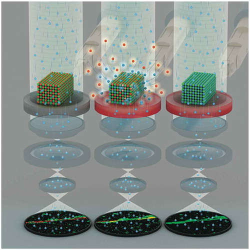
Graphical abstract
1. Introduction
In the last 20 years, several improvements have had a revolutionary impact on the most widely used technique to image and study nanostructures produced through colloidal synthesis, namely transmission electron microscopy (TEM), even in scanning mode (STEM), with its ancillary analytical methods, Energy Dispersive X-Ray Spectroscopy (EDS) and Electron Energy Loss Spectroscopy (EELS). Indeed, TEM/STEM is currently capable to image nanoparticles (NPs) with point resolution better than 0.1 nm, thus providing information on their size, morphology, crystal structure, presence of crystal defects as well as of crystal strain, and composition even at single atomic column scale. These enhanced imaging and analytical capabilities of (S)TEM have been made possible thanks to the development and the availability of a succession of technical improvements: ultra-bright electron sources [Citation1], spherical aberration (CS) correctors for both TEM and STEM [Citation2,Citation3], novel EELS and EDS spectrometers [Citation4,Citation5], novel CMOS electron cameras [Citation6] capable to detect a single electron with sub-pixel precision, which provided either ultrasensitive or ultrafast acquiring and storing images capabilities. The natural consequence of such a constant and dramatic evolution experienced by the (S)TEM field was the massive impulse also received by its in situ capabilities over the last years. Performing in situ (S)TEM basically means that the sample is subject to one or more external stimuli during its observation, and the corresponding changes are observed and studied with proper temporal resolution. Currently, several kinds of stimuli can be provided to (S)TEM samples while they are inside the microscope, such as heating, heating under controlled gaseous atmosphere, cooling, electrical biasing, mechanical indenting or stretching, illuminating, liquid immersion and electrical biasing in an electrochemical cell [Citation7–Citation10]. However, here we will focus our attention on the in situ heating as a driving force to promote a peculiar kind of chemical reactions on samples constituted by crystal NPs. Then, with this regard, an in situ heating experiment requires a dedicated sample holder capable of increasing, controlling and eventually maintaining the temperature of the sample in a most controlled way for extended periods of time. This capability must be paired with two fundamental technical requisites: minimizing the thermally induced spatial drift of the sample and abating the power required to heat it. Until the last decade, these heating holders were either custom-made [Citation11,Citation12] or commercial, with the heat source being constituted by a small furnace surrounding a clamped TEM sample, usually either deposited on an electron-transparent film, eventually supported by a metallic, thermally conductive grid, or directly attached onto the grid [Citation13,Citation14]. In all these cases the temperature was measured either by a thermocouple in contact with the heating element of the holder or by a priori calibration curve, based on the correspondence between heating current and temperature. Even though these holders were designed to minimize the thermal expansion of furnace and sample and to provide thermal isolation of the heating tip from the rest of the holder rod, thus limiting the heat conduction and dissipation, they unavoidably presented three major limitations. First, the size of the furnace and metal grid supporting the sample implied that their thermal dilatation and the corresponding dramatic spatial drift of the TEM sample could not be avoided during thermal ramps, eventually also leading to the local rupture of the thin film supporting the sample. The scale of this drift effect made very hard imaging the samples while their temperature was increased or decreased, and basically impossible both concomitant EDS or EELS compositional analysis and mapping. Second, the temperature was actually measured on the heating element and not on the heated sample, leading to an unavoidable source of uncertainty on the actual thermal value effectively reached by the imaged sample, and causing errors in its measurement up to few tens of degrees. Third, once heating furnace and heated sample reached a steady temperature higher than 80–100°C with a sufficiently low spatial drift to allow imaging and EELS-based analysis or mapping, the huge amount of infrared (IR) radiation produced by the hot parts saturated the EDS detector and made impossible any EDS-based analysis. The view of a furnace-based in situ heating sample holder is shown in .
Figure 1. (a) Tip of an in situ heating furnace-based holder. The dark ring is the furnace, and the hole at its center is the slot where the TEM grid should be inserted and clamped; (b) Graphical representation of a typical heating MEMS. Panels with increasing magnification are used to highlight the position of the small electron-transparent zones. Adapted with permission from [Citation7].
![Figure 1. (a) Tip of an in situ heating furnace-based holder. The dark ring is the furnace, and the hole at its center is the slot where the TEM grid should be inserted and clamped; (b) Graphical representation of a typical heating MEMS. Panels with increasing magnification are used to highlight the position of the small electron-transparent zones. Adapted with permission from [Citation7].](/cms/asset/b01ba86b-ee12-459d-a6b8-b8995a6fda59/tapx_a_1633957_f0001_oc.jpg)
Conversely, the new generations of in situ sample holders that have been realized and made commercially available in recent years are characterized by totally overcoming the furnace-based architecture for thermal annealing and embracing the use of MEMS (microelectromechanical systems) chips technology [Citation15,Citation16]. In these sample holders, the sample substrate, previously constituted by an electron-transparent thin film mechanically supported by the classical metal grid clamped in the middle of the heating furnace, has been abandoned and replaced by a multipurpose chip that integrates the sample support function with both the heating and local temperature measurement capabilities. MEMS are generally constituted by some kinds of thermally conductive materials that in some case can reach temperatures higher than 1000°C, with one or more electron-transparent zones, either empty, possibly covered with a properly chosen material (such as, for instance, amorphous carbon), or constituted by thinner portions of the same chip, which act as a support film for the sample. The heating and the temperature measurement elements are generally provided by two small concentric spiral wirings produced on top of the main body of the MEMS and encircling the electron-transparent zones. They are connected to an external controller that provides the driving current required to reach the desired temperature while continuously measuring the current local temperature. This kind of architecture provides several advantages with respect to the previous furnace-based holders: since the heating element is an actual part of the heating tip constituted by the whole MEMS, both of them dilatate/contract together, thus minimizing the x-y spatial drift to a few of nanometers during the thermal ramps along with aless limited z drift caused by the bulging/unbulging of the MEMS during its heating/cooling ramps. Moreover, the small size of the heating element, its combination with the temperature measuring spiral and its correspondence to the sample deposition zone minimize the uncertainties in monitoring the actual temperature of the sample, which were conversely typical of the furnace-based design. Also, the small size of the heating elements leads to two further advantages, both based on the very low power needed to increase/decrease the produced heat and the related thermal variation: the thermal ramps can be executed in few tenths of second, and the amount of IR radiation produced by using the heating MEMS is much smaller than that produced by the furnace-based in situ sample holders, thus allowing for EDS-based analyses even at high temperature and, if possible, on a certain tilting angle in order to perform 3D chemical maps. The view of a MEMS-based in situ heating sample holder is shown in . Meanwhile, in the last decades, colloidal synthesis emerged as a facile and gainful approach to produce a huge multiplicity of different nanomaterials, permitting to finely tune their shape, size, composition and possible related crystal structure, providing an unprecedented level of control on their chemical and physical properties [Citation17–Citation20]. In this context, (S)TEM emerged as the key imaging and analytical tool to well understand the connection between the physical and chemical properties of these nanostructures and their structure, shape and composition. Then, the improvements of (S)TEM) were strongly beneficial to the fine characterization of colloidal NPs, although a partial limitation remained. Indeed, as colloidal NPs are produced by single or multi-step reactions in a liquid environment, the only way to observe by (S)TEM what was happening during their growth was taking a proper amount of aliquots from the running reaction(s) and study ex situ the changes occurring to their intermediate products, thus ‘freezing’ the reaction(s) at different intermediate steps before the obtainment of the final nanomaterial(s). Then, the kinetics of the reaction became a major parameter: if it was too fast and the reaction started from just liquid reactants, only the final product could be imaged and analyzed. Otherwise, if the reaction either started at least partially by using solid precursors as reagents or/and was not too fast and giving solid intermediate products, only them and the final products could be in-depth studied. To put it in an easier and more concise way: intermediate steps are unavoidably lost for very fast liquid reactions. A similar impediment can be encountered in the study of cation-exchange (CE), which is a popular post-synthetic strategy in colloidal chemistry devoted to partially or totally change the cation sublattice of a NPs’ population while leaving the anions unperturbed. This kind of approach, which is used to obtain ionic NPs difficult to produce by a direct synthesis, generally consists in the fast, direct reaction of a starting population of ionic NPs with one or more cationic species dispersed in a common liquid solution [Citation21–Citation27]. Again, in this kind of scenario, the likely fast rate of reaction hinders collecting information on the evolution of CE before it reaches its final stage. This very hard limitation pushed us to propose a different way to study nanostructures undergoing CE reactions at the solid state and by an in situ S(TEM) approach: in such a case the relevant CE reaction between the starting sample and a second species capable to give rise to CE was triggered by a thermal increase, and the samples’ consequent evolution could be followed directly over time until completion.
Our paper is constituted of four chapters that follow this introduction. The next one aims at highlighting a basic point that justifies the use of the in situ (S)TEM approach to study colloidal NPs reactions at the solid state and shows a fundamental point that will be further developed in the following chapters. Indeed, we describe how different multicomponent NPs can evolve as a consequence of a thermal increase, while those same building blocks would be either stable or evolve quite differently under the same thermal stimulus if they were physically separated on the substrate due to the differences in the chemical reactivity and/or stability in each case [Citation28,Citation29].
This key concept is further expanded in thethird chapter, which presents CE reactions into complex NPs constituted by crystal domains, differentiated by crystal structure and composition but connected by epitaxial relationships. Here we can further define this CE solid-state reaction as an ‘intraparticle’ process [Citation30], even if we show that even here the concomitant occurrence of ‘interparticle’ CE, initially not taken into account in the corresponding paper, cannot be totally ruled out.
In the fourth chapter the concept of in situ CE reaction at the solid state is definitely extended to a more complex phenomenological configuration: two NPs populations, one capable of expelling a chemical species under heating and the other one capable of adsorbing that expelled species, are deposited close-by on the same heating substrate and undergo a CE reaction under heating [Citation31].
The results we present in chapters 2-4 highlight how in situ (S)TEM can successfully address some fundamental points in comprehending the mechanisms that regulate the formation of colloidal nanostructures, despite having been obtained either by MEMS-based in situ heating holders only, by furnace-based holders only or by a combination of furnace-based and MEMS-based ones. It is noteworthy also pointing out that since the developments we report were spread over a quite large time, our choice of approaching this body of work from a semi-historical point of view allows us now reconsidering them all by a different and unifying perspective: in situ (S)TEM-based study emerged not only as an advanced imaging tool to address single and peculiar scientific questions, but as a powerful method that allows understanding and analyzing with unprecedented level of detail the deep mechanism underlying a series of solid-state mechanism and chemical reactions that could not be otherwise understood by any other imaging technique.
In the light of this point of view, the fifth and final chapter of this paper presents a general discussion on both the few articles currently published on the topic and the advantages and limitations of the studies shown in the previous chapters, while also considering possible future and exciting perspectives.
2. Stability of heterostructures under in situ annealing
The first work we report here deals with the in situ annealing of CdSe-Au systems [Citation28]. It was inspired by the interest in understanding how nanostructures containing both CdSe nanorods and Au crystals could evolve under heating, and in particular whether gold moved/migrated on the CdSe nanorods to reach a final stable configuration. Different kinds of starting configuration of the CdSe+Au system were submitted to in situ heating by using a MEMS-based holder, as reported in isolated CdSe nanorods, decorated with Au nanocrystals, i.e. with larger (bigger than 10 nm) Au nanocrystals attached on both tips of the rods and smaller ones (between 1 and 3 nm) attached over the whole rods’ volume; ii) groups of CdSe nanorods connected by large Au nanocrystals grown on their tips and smaller Au nanocrystals attached all over the rods’ length; iii) mix of isolated CdSe nanorods and small Au nanocrystals.
Figure 2. (a, b) Au-decorated CdSe nanorods before (a) and after (b) thermal annealing; (c-f) Isolated and interconnected Au-decorated CdSe nanorods before (c, e) and after (d, f) thermal annealing. CdSe nanorods are connected through Au domains located at the nanorods’ tips; (g, h) CdSe nanorods and Au nanocrystals before (g) and after (h) thermal annealing. After annealing, new Au domains formed at the tip of the CdSe nanorods. Reprinted with permission from [Citation28]. Copyright [2010] American Chemical Society.
![Figure 2. (a, b) Au-decorated CdSe nanorods before (a) and after (b) thermal annealing; (c-f) Isolated and interconnected Au-decorated CdSe nanorods before (c, e) and after (d, f) thermal annealing. CdSe nanorods are connected through Au domains located at the nanorods’ tips; (g, h) CdSe nanorods and Au nanocrystals before (g) and after (h) thermal annealing. After annealing, new Au domains formed at the tip of the CdSe nanorods. Reprinted with permission from [Citation28]. Copyright [2010] American Chemical Society.](/cms/asset/2e915997-e3ec-46bd-ba5c-81abdc2b673b/tapx_a_1633957_f0002_b.gif)
All these systems were in situ heated from room temperature (RT) up to 400°C, monitoring their thermal evolution by HRTEM imaging. shows the evolution after heating at 200–250°C of the different CdSe+Au configurations previously displayed in panels a, c, e, and g, respectively. In the first case, corresponding to isolated nanorods decorated with Au, the heating gave rise to a growth of the larger Au crystal domains located on the tips of the CdSe nanorods, and the disappearance of the smaller Au domains distributed on the length of the nanorods, which migrated toward the tips due to an intrarod ripening, while inter-rod ripening was not observed. In the second configuration, where large Au domains grown on nanorods tips interconnected two or more CdSe nanorods, also decorated with smaller Au nanocrystals, the intra-rod gold ripening was observed once again. In this case the ripening still generated the enlargement of the gold crystals at the tips of the CdSe nanorods, both those connecting two or more nanorods and those located at the far ends of the nanorods assemblies at the expense of the smaller ones decorating the nanorods body, but it is worth noting that a major size increase was observed in the gold domains connecting more than two nanorods. Such a diverse size increase was due to the reduced mobility of the gold from these interconnecting sites and their concomitant capability of maximizing the total interface area shared with the rods they connected. Finally, even heating the mix of small and isolated gold nanoparticles with CdSe nanorods brought to the disappearing of the gold particles and the concomitant formation of large gold domains, again mostly on the tips of the nanorods. Since the observed ripening occurred with both CdSe nanorods and gold crystals at the solid state and under the TEM high vacuum conditions, it was hypothesized that the combined diffusion of gold clusters and atoms could be the most likely mechanism. The clusters diffusion is shown in , where some HRTEM images recorded in the 170–190°C thermal range display the gold clusters (1–3 nm in size) moving over time until reaching the larger gold crystals at the tips of the nanorods and merging.
Figure 3. Motion and coalescence of Au domains on CdSe nanorods during annealing between 170 and 190ºC. White arrows (a-c) indicate the cluster diffusion and coalescence of two Au domains, black arrows (d) indicate the presence of flat Au/CdSe interfaces at the tip of the nanorods after annealing. Reprinted with permission from [Citation28]. Copyright [2010] American Chemical Society.
![Figure 3. Motion and coalescence of Au domains on CdSe nanorods during annealing between 170 and 190ºC. White arrows (a-c) indicate the cluster diffusion and coalescence of two Au domains, black arrows (d) indicate the presence of flat Au/CdSe interfaces at the tip of the nanorods after annealing. Reprinted with permission from [Citation28]. Copyright [2010] American Chemical Society.](/cms/asset/e13ea873-4bc1-4403-9535-fec77d8bee3c/tapx_a_1633957_f0003_b.gif)
This clusters’ diffusion mechanism mostly occurred for gold clusters close to the larger nanocrystals at the tips of the nanorods, but a different mechanism, based on atomic diffusion, was predominant for those located far from them. Here the clusters became smaller until disappearing, while their constituent atoms diffused on the surface of the nanorods until reaching a gold cluster located at the tips, further increasing its size. This mechanism was likely taking place also in the clusters close to the tips, but in this case, the cluster diffusion successfully drives the small cluster to the tips of the nanorods before the atomic diffusion dissolves them. Conversely, a partially different mechanism occurred during the annealing of the mixture of CdSe and Au small particles. Here the most likely mechanism was that some gold particles, located closer to the tips of the nanorods, modified becoming a bridge between two or more rods. Following this, most of the other gold particles dissolved and gave rise to an intra-rod ripening mainly by atomic diffusion, finally leading to the growth of gold domains located on the rods’ tips, like in the previous cases.
Then, the most important result of this work lies in the thermally induced evolution of gold, whose concomitant diffusion by clusters and atoms is dictated by the presence and the interaction with the CdSe nanorods. Indeed, if the gold particles were the sole species present on the heating substrate, their coalescence/sintering in larger and more stable polycrystalline domains would be the only likely phenomenon.
The second case of in situ TEM/EFTEM work we report in this chapter is different and deals with the thermally induced dephosphorylation of Janus-like nanoparticles [Citation29]. The starting heterostructures were obtained by the phosphorylation of copper spherical nanocrystals via a colloidal chemistry route, while the thus-obtained Janus-like dimers were constituted by two crystal domains of faceted, hexagonal close-packed (hcp) Cu3P and a face-centered cubic (fcc) Cu having a spherical shape, respectively ().
Figure 4. Figure 4 (a) ZL image and corresponding EFTEM map (inset) of Janus-like Cu-Cu3P nanoparticles. The presence of Cu and P in the EFTEM map are indicated in red and green, respectively; (b,c) HRTEM images of Janus-like Cu-Cu3P nanoparticles characterized by two different epitaxial relationships between the Cu and Cu3P domains. Adapted with permission from [Citation29]. Copyright [2012] American Chemical Society.
![Figure 4. Figure 4 (a) ZL image and corresponding EFTEM map (inset) of Janus-like Cu-Cu3P nanoparticles. The presence of Cu and P in the EFTEM map are indicated in red and green, respectively; (b,c) HRTEM images of Janus-like Cu-Cu3P nanoparticles characterized by two different epitaxial relationships between the Cu and Cu3P domains. Adapted with permission from [Citation29]. Copyright [2012] American Chemical Society.](/cms/asset/98c7647b-60bb-4e24-a015-293c538a08c2/tapx_a_1633957_f0004_oc.jpg)
The shape and corresponding composition by elemental maps of the two domains displayed in were obtained by the so-called Energy Filtered TEM (EFTEM) mode, which is an imaging technique derived from EELS spectroscopy. Its principle consists in forming the TEM image by selecting the electrons that either did not lose energy or lost a specific amount of it in their scattering with the sample (these two cases correspond to elastic and inelastic scattering, respectively). The image obtained by collecting only the electrons that did not suffer any energy loss is called ‘zero loss’ (ZL) and is characterized by higher contrast with respect to a conventional TEM image, as it the case of . Conversely, an image formed using electrons that lost energy within a proper interval corresponding to the EELS edge of a given element is called an EFTEM image and shows a compositional map of that element. Then, the superposition of multiple EFTEM images related to different elements can be combined to form a chemical map of all the elements whose EELS edges were selected in each EFTEM image. That is the case of the compositional map in the inset of , which was obtained by superposing the EFTEM images of P and Cu and assigning the green and red false colors, respectively. The Fourier analysis of HRTEM images (() highlighted that two diverse epitaxial growths occurred during the phosphorylation that generated the Janus-like dimers, namely, the (111) lattice planes of the Cu were aligned with the (300) planes of Cu3P in agreement with two distinct crystallographic relationships:
with the first and second relations indicating the interface and vector alignment, respectively.
The thermal stability of the Janus-like dimers was studied by heating them using a MEMS-based in situ sample holder. Between 400°C and 500°C the phosphorus sublimation in the TEM vacuum via a dephosphorylation process transformed them into uniform, spherical monocrystals constituted only by fcc Cu, as shown in .
Figure 5. Effects of thermal annealing on the Janus-like nanoparticles. (a) Image of a group of nanoparticles recorded at 450ºC. Dark grey domains indicate the presence of Cu, lighter grey domains are constituted by Cu3P; (b) Image of the same group of nanoparticles after 10 min of annealing at 500ºC. No difference in tone indicating the presence of different domains can be observed; (c) HRTEM image of a Janus-like Cu-Cu3P nanoparticle annealed at 150ºC, with both domains exhibiting fcc crystal structure. Reprinted with permission from [Citation29]. Copyright [2012] American Chemical Society.
![Figure 5. Effects of thermal annealing on the Janus-like nanoparticles. (a) Image of a group of nanoparticles recorded at 450ºC. Dark grey domains indicate the presence of Cu, lighter grey domains are constituted by Cu3P; (b) Image of the same group of nanoparticles after 10 min of annealing at 500ºC. No difference in tone indicating the presence of different domains can be observed; (c) HRTEM image of a Janus-like Cu-Cu3P nanoparticle annealed at 150ºC, with both domains exhibiting fcc crystal structure. Reprinted with permission from [Citation29]. Copyright [2012] American Chemical Society.](/cms/asset/a2535fe9-b158-4659-917d-21109d5e99f9/tapx_a_1633957_f0005_b.gif)
Some noticeable effects were also reported: (a) no melting was observed; (b) the dephosphorylation occurred at different temperatures in the above-mentioned thermal range, i.e. the smaller particles dephosphorylated at lower temperature than the larger ones; (c) the dephosphorylation of the larger nanoparticles (>15 nm) required 60 min of in situ heating to complete at the maximum temperature reached (500°C). The latter result indicated that the dephosphorylation is a kinetical process and, providing that its own activation energy is passed, it can be made slower by decreasing the temperature. Thus, as shown in , the initial Cu3P crystal domain partially changed its structure from hcp to fcc after being annealed at 150°C due to the activation of phosphorus loss, leading to a Janus-like heterostructure. Looking at the crystal features of this newly formed Cu3P1-x domain by Fourier analysis of the corresponding HRTEM images, the relationship between its orientation with respect to the Cu domain can be indicated as:
This ensured the compatibility between {022} lattice spacing of the Cu3P1-x domain, with a spacing of 1.47 Å, and the {112} lattice spacing of the Cu domain, equal to 1.48 Å, and confirmed the match between the new partially dephosphorylated fcc phase and the fcc copper lattice.
Finally, it is worth pointing out that nanocrystals of sole Cu3P were stable and did not lose phosphorous even if annealed at 550°C for more than half an hour. This means that the dephosphorylation was not a purely thermal phenomenon caused by thermal annealing, but it occurred when the copper phosphide was part of dimers containing also a copper domain. This evidence pushed us to study more complex heterostructures such as those reported in the following chapter, in order to better understand how the presence of different compounds constituting nanosized heterostructures could generate a compositional change triggered by their in situ thermal increase.
3. In situ diffusion and cation-exchange intra-nanostructures
In 2013, we showed how to modify complex nanosized heterostructures by thermal annealing performed once again by an in situ (S)TEM/EFTEM approach. The difference from what reported in the previous chapter lays in the complexity of the processes triggered by annealing, which were not limited to the atomic rearrangement or the simple sublimation of a single atomic species, but manifested as an actual change in composition triggered by the diffusion of different atomic species within the heterostructures [Citation30].
The starting materials were nano-sandwiches prepared by a colloidal route and constituted by a central crystal domain of copper phosphide (Cu3P) between two crystal domains of cadmium selenide (CdSe), as shown in .
Figure 6. (a) HRTEM image of packed CdSe/Cu3P/CdSe nano-sandwiches. The [0001] stacking of Cu3P and CdSe (individuated by the variation in electron contrast) is clearly visible; (b) EDS line profile over a HAADF-STEM image of a single nano-sandwich, showing the elemental distribution across its width; (c) HRTEM image showing the epitaxial relationship between CdSe and Cu3P at the interface of the nano-sandwich; (d) 2D-FFT patterns of the sole Cu3P and CdSe phases (labeled in red and blue, respectively) and of both phases. The combined FFT pattern highlights the structural correspondence between phases. Reprinted with permission from [Citation30]. Copyright [2013] American Chemical Society.
![Figure 6. (a) HRTEM image of packed CdSe/Cu3P/CdSe nano-sandwiches. The [0001] stacking of Cu3P and CdSe (individuated by the variation in electron contrast) is clearly visible; (b) EDS line profile over a HAADF-STEM image of a single nano-sandwich, showing the elemental distribution across its width; (c) HRTEM image showing the epitaxial relationship between CdSe and Cu3P at the interface of the nano-sandwich; (d) 2D-FFT patterns of the sole Cu3P and CdSe phases (labeled in red and blue, respectively) and of both phases. The combined FFT pattern highlights the structural correspondence between phases. Reprinted with permission from [Citation30]. Copyright [2013] American Chemical Society.](/cms/asset/6f693f18-1f02-493d-87bd-73eaf6d700ef/tapx_a_1633957_f0006_oc.jpg)
Both CdSe and Cu3P domains had a hexagonal crystal structure and belonged to the same space group. Before any reaction took place, as shown in (a), the double interface in the CdSe/Cu3P/CdSe was revealed as the two phases generating different electron scattering and related absorption. The composition of nano-sandwiches was determined by STEM-EDS line scan, as reported in . Besides, the careful Fourier analysis of the CS-corrected HRTEM images () indicated that the three domains constituting the nano-sandwiches grew in epitaxial relationship between them, that is:
with the first relation indicates the interface alignment, and the second relation the vector one.
To perform the in situ TEM reaction the samples were heated at 300°C, 350°C and 400°C, respectively, by using a furnace-based sample holder. (-) displays what happened to a nano-sandwich at these three thermal steps from a structural point of view.
Figure 7. HRTEM images showing the thermal evolution of a single CdSe/Cu3P/CdSe nano-sandwich upon thermal annealing. (a) The initial structure is maintained from RT to 300ºC; (b) at 350ºC the CdSe cannot be observed anymore in the lateral domains and is substituted by Cu2Se domains; (c) at 400ºC even Cu3P cannot be observed anymore in the central domain and the sole Cu2Se phase can be observed in the newly formed single crystal. Scale bars correspond to 5 nm. Reprinted with permission from [Citation30]. Copyright [2013] American Chemical Society.
![Figure 7. HRTEM images showing the thermal evolution of a single CdSe/Cu3P/CdSe nano-sandwich upon thermal annealing. (a) The initial structure is maintained from RT to 300ºC; (b) at 350ºC the CdSe cannot be observed anymore in the lateral domains and is substituted by Cu2Se domains; (c) at 400ºC even Cu3P cannot be observed anymore in the central domain and the sole Cu2Se phase can be observed in the newly formed single crystal. Scale bars correspond to 5 nm. Reprinted with permission from [Citation30]. Copyright [2013] American Chemical Society.](/cms/asset/b168e06e-4f8f-4741-b32e-4d90002b6ff2/tapx_a_1633957_f0007_oc.jpg)
Up to 300°C no difference could be appreciated with respect to the structure observed at RT, while at 350°C the two external CdSe domains started to show a crystal structure ascribable to fcc rather than the initial hcp. This change was accompanied by a variation within lattice set distances, which became compatible with those of a Cu2Se phase, having been all other possible phases obtained by a combination of Cd, P, Cu and P carefully discarded. However, at 350°C, it was still possible recognizing the presence of three separate crystal domains as in the starting heterostructure, with the central one still displaying structural parameters ascribable to the copper phosphide. It is worth noting that the likely transition of the two external domains from the hexagonal CdSe to the cubic Cu2Se required that at least the central domains acted as a source of copper cations, with their consequent depletion of copper. Fourier analysis still identified the central and external domains as Cu3P and Cu2Se, respectively, because their lattice features fell within the lattice resolution provided by the HRTEM, even if the crystal phases were very likely sub-stoichiometric in copper (i.e. Cu3-xP and Cu2-xSe) due to the ongoing diffusion of Cu from the central to the external domains. At 400°C, the crystal structure changed further: the three distinct domains did not exist anymore and were replaced by a single nanocrystal displaying lattice spacing compatible with Cu2Se. The change in composition occurring to the nano-sandwiches was also confirmed by the EFTEM maps collected on a large ensemble and reported in , where the evolution from RT up to 400°C was definitely clear.
Figure 8. ZL images and EFTEM elemental maps of a group of nano-sandwiches recorded during a thermal annealing from RT to 400ºC and showing the progressive disappearance of P and Cd and the concomitant expansion of Cu. Scale bars correspond to 100 nm. Reprinted with permission from [Citation30]. Copyright [2013] American Chemical Society.
![Figure 8. ZL images and EFTEM elemental maps of a group of nano-sandwiches recorded during a thermal annealing from RT to 400ºC and showing the progressive disappearance of P and Cd and the concomitant expansion of Cu. Scale bars correspond to 100 nm. Reprinted with permission from [Citation30]. Copyright [2013] American Chemical Society.](/cms/asset/2af0739f-a3c9-4018-b89b-5910bcac17e9/tapx_a_1633957_f0008_oc.jpg)
Indeed, at 350°C, the signal of phosphorus was still detected from the central part of the heterostructures, and those of cadmium and copper were still clear, with the latter expanding towards the external crystal domains. This allows hypothesizing that Cu partially substituted Cd, triggering the change from the hexagonal crystal structure of CdSe to the cubic Cu2Se. However, the concomitant presence of Cu and Cd in the external domains indicated that a CE was still in progress at that temperature. Conversely, at 400°C the change in composition of both central and external domains was completed: they had become a unique domain that presented no trace of Cd and P, whose sublimation was triggered by the diffusion of Cu that totally exchanged Cd in the external domains and by Se that substituted P in the central one.
A further important consideration has to be done in observing the image of the entire group of nanostructures that remained on the TEM support after the annealing at 400°C. Several among the original nano-sandwiches totally disappeared from the support and speculating about the most likely cause of this phenomenon can add an important insight into the general behavior of this system. This deduction had not been reported in the original paper but seems logical in the light of the experimental results that we observed at a later time and which are reported in the following chapter. Out of the four elements constituting the initial nano-sandwiches (Cu, P, Cd, Se) two (Cd and P) have been shown to sublimate as a consequence of the crisscrossed diffusion of the latter two (Cu and Se), which are maintained after the thermal treatment and finally give rise to single domains of Cu2Se. The former comes from just the central domains, where it was with a ratio of 3 to 1 per phosphorus atom, to change into a ratio of 2 to 1 per selenium atom. Now, neglecting the possible difference in density of the two compounds, we can still consider that the volume of each of the three initial domains constituting the nano-sandwiches was roughly the same. This means that, even if the Cu to P ratio (3 to 1) in the starting central domain was higher than the Cu to Se ratio of the whole final nanoparticles (2 to 1), it is debatable whether all the copper contained in the initial Cu3P central domain was actually sufficient to support the completion of the reaction leading to the formation of Cu2Se over the whole final structure. Conversely, the selenium coming from the external domains started from a 1 to 1 ratio per cadmium atom and changed to a 1 to 2 ratio per copper atom after thermal treatment. This immediately leads to qualitatively consider that, if on one side the initial amount of Se contained into the original external domains of CdSe could be enough to form the final structure of Cu2Se, this consideration is harder to sustain when considering the copper amount moving from the sole central domain to the external ones to give rise to a homogeneous final structure. Thus, if the available copper was not enough to form the final Cu2Se nanoparticles having the same volumes of the starting nano-sandwiches, the missing copper should have been provided by other sources, namely neighbor heterostructures, by a kind of inter-structure diffusion. However, the consequence of a similar event would have been the unbalancing of the atomic arrangement in the structures acting as donors of copper, likely leading to sublimation of the remaining elements and the disappearance of the whole ‘donor’ nanostructures.
The most important conclusion of this work lied in the fact that we observed the copper diffusion from the central to the external domains, and that now we could start to think that likely some additional copper came from close-by heterostructures, a mechanism that we did not initially suppose in [Citation30]. In any case, thermally activated copper diffusion acted as the pivotal driving force in changing the structure and composition of the initial nanostructures. This fundamental point was also reported in our work: nanoparticles constituted by sole CdSe and sole Cu3P did not show any kind of thermally induced evolution in the range of temperatures where the nano-sandwiches constituted by the ensemble of the two compounds change to single Cu2Se nanocrystals. This definitely indicated that the phenomena generating this evolution were the diffusion and the associated cation-exchange between Cd and Cu activated by the thermal annealing of the nano-sandwiches heterostructures.
4. In situ cation-exchange among separate nanostructures
As reported in the previous chapter, in [Citation30] we observed that the copper could diffuse and give rise to cation exchange with Cd within and likely also among the nano-sandwiches heterostructures. The intraparticle diffusion was not too surprising, since it was already known that copper chalcogenides were prone to CE reactions due to the occurrence of Cu vacancies that could facilitate the cation diffusion and the subsequent exchange [Citation32]. Besides, other studies showed that post-synthetic processes could tune the excitonic and plasmonic properties of copper chalcogenides nanocrystals by changing their stoichiometry, and in particular by generating a copper deficit [Citation33,Citation34]. This, together with what observed during the in situ experiments on nano-sandwiches, inspired us to study if this tendency could be exploited for a totally inter-structure diffusion, i.e. pairing a nanosized population capable of acting as copper atoms reservoir/donor with and another one capable of collecting the copper provided from the first population and undergoing a CE reaction at the solid state. In the light of what reported in above-cited papers, our first choice for the population acting as copper ‘donor’ was Cu2Se, and CdSe as the ‘acceptor’ [Citation31].
The first step of our work was checking what happens to spherical Cu2Se nanocrystals of 7 nm in size when they were in situ heated in the (S)TEM. As displayed in , a multiplicity of effects was observed: (a) both CS-corrected HRTEM imaging performed on the same single crystal before and after the annealing at 400°C (panels a, b) and Electron Diffraction (ED) patterns measured by illuminating several nanocrystals (panel c) showed that the Cu2Se nanocrystals underwent an appreciable decrease of their fcc lattice constant; (b) the High Resolution EEL (HREEL) low-loss spectrum, i.e. that acquired from an ensemble of many Cu2Se nanocrystals and very close (less than 2 eV of electron energy loss) to the ZL peak thanks to a monochromatized STEM, indicated that after the heating the compound shows a low-loss feature at about 1.1eV (panels e, f), corresponding to a localized surface plasmon not present before the heating. Moreover, the EEL spectrum analysis of the heated spectrum displayed that after the heating about the 10% of the copper was lost; (c) the HREEL spectrum was then simulated by density functional theory (DFT) (panel g), considering both the Cu2Se and Cu1.9Se stoichiometry, as experimentally determined. Such a simulated spectrum of the copper selenide sub-stoichiometric in Cu clearly exhibited the appearance of the low-loss feature experimentally observed by HREELS.
Figure 9. (a, b) HRTEM images of a single Cu2Se nanoparticle at RT (a) and after thermal annealing (b). The slight variation observed in d-spacing indicates the lattice shrinking caused by thermal-activated release of Cu atoms; (c) integrated ED patterns of a Cu2Se nanoparticles at RT (magenta) and after thermal annealing (orange). The upward shift of the diffraction peaks confirms the lattice shrinking caused by the partial Cu depletion; (d) STEM image showing a group of Cu2-xSe nanoparticles. The blue rectangle indicates the area investigated by HREELS; (e, f) HREEL spectra of the area indicated in (d). No features can be observed in the spectrum recorded at RT (e), while a low-energy peak caused by a low-energy plasmon appears in the spectrum recorded after annealing; (g) DFT simulation of HREEL spectra of stoichiometric (black) and depleted (red) Cu2Se nanoparticles. The red (depleted) spectrum features a peak at the same energy as the experimental peak observed after annealing (f). Reprinted with permission from [Citation31]. Copyright [2016] American Chemical Society.
![Figure 9. (a, b) HRTEM images of a single Cu2Se nanoparticle at RT (a) and after thermal annealing (b). The slight variation observed in d-spacing indicates the lattice shrinking caused by thermal-activated release of Cu atoms; (c) integrated ED patterns of a Cu2Se nanoparticles at RT (magenta) and after thermal annealing (orange). The upward shift of the diffraction peaks confirms the lattice shrinking caused by the partial Cu depletion; (d) STEM image showing a group of Cu2-xSe nanoparticles. The blue rectangle indicates the area investigated by HREELS; (e, f) HREEL spectra of the area indicated in (d). No features can be observed in the spectrum recorded at RT (e), while a low-energy peak caused by a low-energy plasmon appears in the spectrum recorded after annealing; (g) DFT simulation of HREEL spectra of stoichiometric (black) and depleted (red) Cu2Se nanoparticles. The red (depleted) spectrum features a peak at the same energy as the experimental peak observed after annealing (f). Reprinted with permission from [Citation31]. Copyright [2016] American Chemical Society.](/cms/asset/99ee11e1-79a5-4515-9a1d-dd8f2bfe37e2/tapx_a_1633957_f0009_oc.jpg)
The ensemble of these results clearly indicated that, as a consequence of the in situ (S)TEM heating at 400°C, the Cu2Se nanocrystals expelled about the 10% of their copper and underwent an isostructural contraction of the fcc lattice, as well as the appearance of the surface plasmon at 1.1 eV.
The second step we performed was trying to exploit the copper expelled by the Cu2Se nanocrystals to engage it in a local CE reaction at the solid state with a second population of nanostructures, known to be prone to undergo CE with Cu, such as the CdSe reported in the previous chapter. With this aim, we spread the 7 nm spherical nanocrystals of Cu2Se and CdSe monocrystalline nanorods on the same in situ heating substrate and annealed them together up to 400°C, as previously made for the sole Cu2Se nanocrystals. displays the STEM-High Angular Annular Dark Field (HAADF) images together with the EFTEM compositional maps of this mix of the two nanopopulations before and after their thermal annealing, being the STEM-HAADF contrast only due to the thickness and the atomic number of the imaged sample, i.e. without any kind of diffraction contrast.
Figure 10. (a-d) HAADF-STEM images and EFTEM maps of Cu2Se nanospheres and CdSe nanorods at RT (a, b) and after annealing at 400ºC (c, d). Cu and Cd are indicated in green and red, respectively; (e) HRTEM image and corresponding 2D-FFT pattern of a representative hcp CdSe nanorod at RT; (f) HRTEM image and corresponding 2D-FFT pattern of the same nanorod after annealing to 400ºC. Its length is slightly diminished and its crystal structure has changed to fcc. Adapted with permission from [Citation31]. Copyright [2016] American Chemical Society.
![Figure 10. (a-d) HAADF-STEM images and EFTEM maps of Cu2Se nanospheres and CdSe nanorods at RT (a, b) and after annealing at 400ºC (c, d). Cu and Cd are indicated in green and red, respectively; (e) HRTEM image and corresponding 2D-FFT pattern of a representative hcp CdSe nanorod at RT; (f) HRTEM image and corresponding 2D-FFT pattern of the same nanorod after annealing to 400ºC. Its length is slightly diminished and its crystal structure has changed to fcc. Adapted with permission from [Citation31]. Copyright [2016] American Chemical Society.](/cms/asset/1e982886-0341-4e66-a567-5c4d503b20ba/tapx_a_1633957_f0010_oc.jpg)
It can be observed (panel a, b and c, d) that while the Cu2Se nanocrystals did not show any apparent morphological change after heating, conversely the CdSe monocrystalline nanorods became shorter, their mean length going from 35 to 22 nm while keeping their diameter almost constant. This shrinkage of the nanorods corresponds to an overall volume decrease of more than 40%, much higher than what expected in the case of a pure contraction of the crystal lattice passing from the hcp CdSe to the fcc Cu2Se structure with a supposed total preservation of the Se anion sublattice. Then, the additional shrinking that we observed was caused by the partial loss of Se anions by the nanorods during the compositional and structural rearrangement due to the CE between Cd and Cu. This is very likely due to an insufficient amount of copper coming from the Cu2Se and needed to perform a total Cd → Cu replacement. Then, a partial sublimation of Se anions was needed to preserve the atomic charge balance in the rods after the CE took place. In any case, e, f also displays the change of crystal structure of the starting hcp CdSe nanorods into fcc Cu2Se after CE, as imaged by Cs-corrected HRTEM. Indeed, the lattice change maintained the close-packing direction, i.e. the [0001] direction in the initial hcp CdSe structure became the [111] in the final fcc Cu2Se nanorods, even though this transformation required also that the Se sublattice rearranged to follow this structural change. The EFTEM compositional maps further confirmed what happened: before the heating copper (green) and Cd (red) were located just in correspondence to the Cu2Se nanocrystals and the CdSe nanorods, respectively, while after heating the signal of copper was found in both the nanocrystals and nanorods and, and no Cd signal was detected.
Further experiments where performed, using as acceptor nanostructures hcp CdSe nanowires instead of CdSe nanorods, as shown in .
Figure 11. ZL images, corresponding EFTEM elemental maps (Cu and Cd are indicated in green and red, respectively) and HRTEM images of Cu2−xSe nanoparticles and CdSe nanowires recorded at RT (a-c), 350ºC (d-f) and after annealing to 400ºC (g-i). No variation can be observed in the ZL images (a, d, g), while the diffusion of Cu and the ongoing Cu-to-Cd CE are evident from EFTEM maps (b, e, h). HRTEM images of a CdSe nanowire show its structural evolution from a hcp structure (c, RT) to a defective ((f), 350ºC) and well-defined fcc structure ((i), 400ºC). Reprinted with permission from [Citation31]. Copyright [2016] American Chemical Society.
![Figure 11. ZL images, corresponding EFTEM elemental maps (Cu and Cd are indicated in green and red, respectively) and HRTEM images of Cu2−xSe nanoparticles and CdSe nanowires recorded at RT (a-c), 350ºC (d-f) and after annealing to 400ºC (g-i). No variation can be observed in the ZL images (a, d, g), while the diffusion of Cu and the ongoing Cu-to-Cd CE are evident from EFTEM maps (b, e, h). HRTEM images of a CdSe nanowire show its structural evolution from a hcp structure (c, RT) to a defective ((f), 350ºC) and well-defined fcc structure ((i), 400ºC). Reprinted with permission from [Citation31]. Copyright [2016] American Chemical Society.](/cms/asset/7baa298c-c1aa-4438-9420-c6bd1ca0ba23/tapx_a_1633957_f0011_oc.jpg)
The results found in terms of both compositional and structural transition revealed that the morphology change of CdSe from nanorods to nanowires did not substantially affect any parameter related to the investigated in situ CE. However, looking at both the compositional maps and Cs-corrected HRTEM images collected at 350°C, we were able to determine what happened to the CdSe nanowires during the progress of CE between cadmium and copper. At that temperature cadmium was leaving the nanowires and being replaced by copper, thus modifying the lattice structure to fcc and leading to the appearance of pervasive stacking faults affecting the crystal structure undergoing this CE-driven modification.
Some final conclusion could be made about the phenomenon described above. First, it should be reminded that all the experiments were performed inside the (S)TEM column, meaning that all the species that were leaving the nanostructures undergoing any kind of transformation (namely, the copper expelled by the Cu2Se and the cadmium replaced by the copper into the nanorods/nanowires, together with some selenium) were subject to a high dynamic vacuum that likely acted as a sink for anything that was sublimated and not reintroduced in the nanostructures by the end of the CE reaction. This was, in fact, the case of both Cd and Se: no trace of the former was found in the sample after the solid-state reaction’s completion, while Se was detected only in nanorods/nanowires (maps not shown). Conversely, once expelled from the copper selenide nanoparticles, copper diffused over the heated substrate until reaching the CdSe nanorods/nanowires where it triggered the CE reaction at the solid state. This scenario was further corroborated by the fact that even nanorods/nanowires not in direct contact with Cu2Se particles underwent CE, thus indicating that the migration mechanism invoked for copper on the heated substrate was the most likely occurred. Conversely, it is hard believing that copper could have first sublimated and then re-deposited on the TEM grid: first due to the presence of a cold finger acting as a cryo-trap for any sublimated species in the (S)TEM column near the sample; then, because, even if the vapor-phase copper remained suspended in proximity to the sample surface despite the (S)TEM cryo-trap and the high vacuum pumps, it should somehow re-deposit on a surface that is more than 300ºC hotter than the rest of the TEM column. Also, under this circumstance, the re-deposition of the thin cloud of vapor-phase copper should have likely triggered a ubiquitous presence of copper nanoparticles all over the TEM substrate, and this was never the case. A second fundamental point concerns the oxidation state of the copper expelled from the Cu2Se nanoparticles and diffusing over the heated TEM substrate. It is unlikely supposing that it left the source nanoparticles as charged ion rather than a zerovalent atomic copper (Cu (0)). Considering that copper was present as a cation in the Cu2Se NPs, it was likely reduced to the zerovalent state by the electron beam after having been expelled on the substrate, until turning back to a cationic state due to intra-lattice charge transfer during the copper-to-cadmium exchange taking place in the CdSe nanostructures. The possibility of an influence by the substrate over the migration of copper was ruled out after the same phenomenon was observed during thermally driven CE reactions at the solid-state performed on C and Si3N4 amorphous substrates. Indeed, the amorphous nature of the substrates corroborated the hypothesis that Cu(0) atoms encountered an isotropic and homogenous chemical environment during their migration, i.e. their superficial diffusion did not proceed along any preferential direction, which would have manifested as a spatially anisotropic and orientation-dependent CE that was never observed.
5. Conclusions and future perspectives
The previous chapters aimed at providing with a general review of the results obtained in performing CE reactions at the solid state by an in situ heating (S)TEM approach. To the best of our knowledge, the above-reported works, together with few further interesting and recent ones [Citation35–Citation37], constitute the whole literature currently available on such a kind of investigations performed by in situ (S)TEM methods. In particular, the paper of Yalcin et al. [Citation35] reports that in nanodumbell-shaped heterostructures constituted by CdSe and PbSe undergoing in situ heating between 160°C and 200°C, CE occurred at the interface between the two semiconducting single crystal domains. Here, upon thermal stimulus, the Cd evaporated and was replaced by Pb cations possibly coming from molecules of Pb-oleate adsorbed on the heterostructures surface, finally resulting in the growth of the PbSe domain at the expense of the CdSe one, with a mechanism not too far from that reported in our previous study [Citation30]. Besides, the results reported in the paper of Buha et al. [Citation36] have been obtained using an approach very similar to the one we reported in [Citation31]. Indeed, in such a work 2D platelets of Bi2Se3 and Bi2Te3 were deposited on a common substrate of amorphous carbon together with Cu NPs. After heating this mixed nanopopulation, the Cu NPs were partially or totally sublimated, due to the release of copper that intercalated both Bi2Se3 and Bi2Te3 nanoplatelets. It is also interesting noticing that: (a) the intercalation occurred at 250°C for Bi2Se3 and at 350°C for Bi2Te3 nanoplatelets, not giving rise to the same final structural arrangement, and (b) upon further heating at 350°C only the Bi2Se3 nanoplatelets underwent a partial CE to Cu2-xSe, i.e. just in a region of the already intercalated nanoplatelets. Finally, it is noteworthy mentioning the work of Zhang et al. [Citation37], dealing with an electrically driven in situ CE reaction. Here, a single CdS nanowire was put between two electrodes, one of which was constituted by copper and acting as a cations source. When a voltage is applied to such a system and a current flows through the single nanostructure, a series of subsequent steps give rise to a CE reaction: first, the most external Cd atoms constituting the CdS wire were expelled from its surface due to the heating, leading to a very pronounced local thermal increase, reaching temperatures higher than 600°C. The sublimation of these Cd atoms occurred while keeping the sulfur anionic sublattice unaltered and resulted in the appearance of cation vacancies at the wire surface, in turn generating the diffusion of the inner Cd cations to the surface, thus leaving vacancies in the subsurface. Then, the Cd atoms that left the CdS nanowire were replaced by copper cations coming from the Cu electrode and driven by the electric field. The process basically led to a final core-shell nanostructure constituted by a CdS core surrounded by a Cu2S shell, whose thickness depends mainly on the duration of the in situ electrical stimulus.
Further progress and wider diffusion of the in situ (S)TEM-based approaches at the solid-state require that some fundamental points are successfully investigated more in-depth: on one hand they concern practical technical limitations, in particular when the mechanism exploited for obtaining the CE reaction is based on thermally driven diffusion of exchanging species, and on the other some general considerations that unavoidably raise in reviewing the results obtained by these approaches.
Thus, looking at current results by a deep and critical approach, some technical, tightly related limitations stand out. Indeed, the first possible issue is represented by the cleanness of the as-prepared materials (i.e. different species of colloidal nanocrystals spread on the same (S)TEM heating substrate and acting as cation donors and acceptors, respectively) intended to undergo CE reactions under thermal stimulus. In fact, the presence of superficial residues of organics coming from the materials’ syntheses (a typical issue encountered in materials prepared by colloidal chemistry routes) can dramatically alter and possibly totally hinder the reactions; thus, a proper preventive cleaning of the materials is fundamental. Usually, this goal can be reached by heating them for a few hours at a temperature around 130°C under high vacuum and/or proceeding with a gentle plasma cleaning. An insufficient cleaning will be indicated by the residual presence of organic residuals acting as a major source of carbon contamination under the electron beam irradiation and forming a thick layer of carbon that will progressively affect the imaging quality and very likely inhibit the atomic mobility and, consequently, the CE reaction. However, these cleaning procedures can be used only if, as in the above-reported cases, the energy they provide to the materials is lower than the activation energy for the CE reaction: if the activation energy was exceeded as a consequence of the heating under vacuum or the plasma cleaning, the CE reaction would start during the cleaning and prior to the intended beginning of the proper experiment.
The second and more fundamental aspect of our studies concerns the insights obtained by using the above-reported approach and deserves some further consideration. As extensively clarified in the introduction paragraph, the reason behind intra- and inter-nanostructures in situ CE studies was collecting information otherwise not attainable about the intermediate states of a given reaction in order to fully understand its mechanism. As we already mentioned in the introduction, usually a CE reaction is performed in a liquid solution and, if it is not too fast, its intermediate states could be studied by either stopping it at different times before completion or taking batch aliquots from the reaction at different times up to the reaction accomplishment, then studying shape, crystal structure and composition of the intermediate products. Conversely, if the reaction is too fast to be stopped during its evolution, this approach is unfeasible and only the starting (if at the solid state) and the final stages of the reaction could be studied, i.e. possibly before its beginning and in any case after its completion. That being said, the most crucial and puzzling question is whether a CE reaction performed by an in situ (S)TEM approach (thus, under the high vacuum of a (S)TEM column) at the solid state, as shown in the previous chapters 3 and 4, occurs like a CE reaction in liquid solution starting from the same nanostructures and that, by a posteriori comparison, gives rise to the same final product. Providing a satisfying answer to this question looks, at the present state, very difficult by a purely experimental approach, since following dynamically a CE reaction occurring in liquid seems a very challenging effort. Indeed, even taking for granted the feasibility of the very hard task of carefully reproducing a slow CE reaction in liquid solution by using an in situ S(TEM) liquid specimen holder, the intrinsic limited spatial resolution expected for this kind of imaging technique should be lower than the one needed to distinguish the fine details that are necessary to understand in-depth how the reaction takes place [Citation38,Citation39]. Together with that, the actual final resolution is further worsened by the contribution of the expected Brownian motion of the particles in liquid. Besides, apart from such an intrinsic limited spatial resolution that would be unavoidable in imaging NPs in a liquid environment, the latter would make basically impossible obtaining compositional information from the sole-immersed objects. Moreover, even though such a kind of experiment was somehow approachable, a further complication to take into very careful account would be the interaction between the electron beam and both the liquid solution’s components and the substrate, i.e. the thin windows that seal the liquid sample holder. These interactions are in fact expected to very likely give rise to a series of possible chemical, reactive species that could in turn rapidly modify the composition/reactivity of the liquid solution where the reaction was occurring. Thus, the possible response to the question about how far, or how close, a thermally driven CE reaction, performed in situ, under high vacuum and at the solid state, is to the corresponding one performed in liquid solution remains the most crucial point to address to further shed light on both the mechanisms ruling the CE reactions and the capability of the in situ (S)TEM to effectively investigate them. Likely, a mixed approach developed by combining a wise comparison of experimental results obtained by different ways and theoretical simulations, such as that reported in [Citation35,Citation40], could provide sufficiently reliable responses.
Acknowledgments
Graphical abstract was produced by Heno Hwang, scientific illustrator at KAUST, who is very gratefully acknowledged.
Disclosure statement
No potential conflict of interest was reported by the authors.
Additional information
Funding
Related Research Data
References
- Freitag B, Knippels G, Kujawa S, et al. First performance measurements and application results of a new high brightness Schottky field emitter for HR-S/TEM at 80-300kV acceleration voltage. Microsc Microanal. 2008;14:529–553.
- Haider M, Uhlemann S, Schwan E, et al. Electron microscopy image enhanced. Nature. 1998;392:768–769.
- Krivanek OL, Dellby N, Lupini AR. Towards sub-Angstrom eelectron beams. Ultramicroscopy. 1999;78:1–11.
- Gubbens A, Barfels M, Trevor C, et al. The GIF quantum, a next generation post-column imaging energy filter. Ultramicroscopy. 2010;110:962–970.
- Von Harrach HS, Dona P, Freitag B, et al. An integrated multiple silicon drift detector system for transmission electron microscopes. J Phys: Conf Ser. 2010;241:012015.
- Ruskina RS, Yub Z, Grigorieff N. Quantitative characterization of electron detectors for transmission electron microscopy. J Struct Biol. 2013;184:385–393.
- Casu A, Sogne E, Genovese A, et al. The new youth of the in situ transmission electron microscopy. In: Stanciu SG, editor. Microscopy and analysis. ISBN 978-953-51-2579-2, InTech Editions; 2016. DOI:10.5772/63269
- Zheng H, Meng YS, Zhu Y. Frontiers of in situ electron microscopy. MRS Bull. 2015;40:12–18.
- Taheri ML, Stach EA, Arslan I, et al. Current status and future directions for in situ transmission electron microscopy. Ultramicroscopy. 2016;170:86–95.
- Hansen TW, Wagner JB, Eds.. Controlled atmosphere transmission electron microscopy. Springer International Editing; 2016. DOI:10.1007/978-3-319-22988-1
- Ruault MO, Chaumont J, Bernas H. Transmission electron microscopy study of ion implantation induced Si amorphization. Nucl Instrum Methods Phys Res. 1983;209:351–356.
- Heinemann K, Poppa H. Direct observation of small cluster mobility and ripening. Thin Solid Films. 1976;33:237–251.
- Chen SH, Zheng LR, Carter CB, et al. Transmission electron microscopy studies on the lateral growth of nickel silicides. J Appl Phys. 1985;57:258–263.
- Dannenberg R, Stach E, Groza JR, et al. TEM annealing study of normal grain growth in silver thin films. Thin Solid Films. 2000;379:133–138.
- Zhang M, Olson EA, Twesten RD, et al. In situ transmission electron microscopy studies enabled by microelectromechanical system technology. J Mater Res. 2005;20:1802–1807.
- Allard LF, Bigelow WC, Jose-Yacaman M, et al. A new MEMS-based system for ultra-high-resolution imaging at elevated temperatures. Microsc Res Tech. 2009;72:208–215.
- Milliron DJ, Hughes SM, Cui Y, et al. Colloidal nanocrystal heterostructures with linear and branched topology. Nature. 2004;430:190–195.
- Pang X, Zhao L, Han W, et al. A general and robust strategy for the synthesis of nearly monodisperse colloidal nanocrystals. Nat Nanotechnol. 2013;8:426–431.
- Costi R, Saunders AE, Banin U. Colloidal hybrid nanostructures: a new type of functional materials. Angew Chem Int Ed. 2010;49:4878–4897.
- Yin Y, Alivisatos AP. Colloidal nanocrystal synthesis and the organic-inorganic interface. Nature. 2005;437:664–670.
- Gupta S, Kershaw SV, Rogach AL. 25th Anniversary article: ion exchange in colloidal nanocrystals. Adv Mater. 2013;25:6923−6944.
- Son DH, Hughes SM, Yin YD, et al. Cation exchange reactions in ionic nanocrystals. Science. 2004;306:1009−1012.
- De Trizio L, Manna L. Forging colloidal nanostructures via cation exchange reactions. Chem Rev. 2016;116:10852–10887.
- Beberwyck BJ, Surendranath Y, Alivisatos AP. Cation exchange: a versatile tool for nanomaterials synthesis. J Phys Chem C. 2013;117:19759−19770.
- Rivest JB, Jain PK. Cation exchange on the nanoscale: an emerging technique for new material synthesis, device fabrication, and chemical sensing. Chem Soc Rev. 2013;42:89−96.
- Luther JM, Zheng HM, Sadtler B, et al. Synthesis of PbS nanorods and other ionic nanocrystals of complex morphology by sequential cation exchange reactions. J Am Chem Soc. 2009;131:16851−16857.
- Li H, Zanella M, Genovese A, et al. Sequential cation exchange in nanocrystals: preservation of crystal phase and formation of metastable phases. Nano Lett. 2011;11:4964–4970.
- Figuerola A, van Huis M, Zanella M, et al. Epitaxial CdSe-Au nanocrystal heterostructures by thermal annealing. Nano Lett. 2010;10:3028–3036.
- De Trizio L, Figuerola A, Manna L, et al. Size-tunable, hexagonal plate-like Cu3P and Janus-like Cu-Cu3P nanocrystals. ACS Nano. 2012;6:32–41.
- De Trizio L, De Donato CA, Genovese A, et al. Colloidal CdSe/Cu3P/CdSe and their evolution upon thermal annealing. ACS Nano. 2013;7:3997–4005.
- Casu A, Genovese A, Manna L, et al. Cu2Se and Cu nanocrystals as local sources of copper in thermally activated in situ cation exchange. ACS Nano. 2016;10:2406–2414.
- Comin A, Manna L. New materials for tunable plasmonic colloidal nanocrystals. Chem Soc Rev. 2014;43:3957−3975.
- Dorfs D, Härtling T, Miszta K, et al. Reversible tunability of the near-infrared valence band plasmon resonance in Cu2‑xSe nanocrystals. J Am Chem Soc. 2011;133:11175−11180.
- Kriegel I, Jiang C, Rodríguez-Fernández J, et al. Tuning the excitonic and plasmonic properties of copper chalcogenide nanocrystals. J Am Chem Soc. 2012;134:1583−1590.
- Yalcin AO, Fan Z, Goris B, et al. Atomic resolution monitoring of cation exchange in CdSe-PbSe heteronanocrystals during epitaxial solid–solid–vapor growth. Nano Lett. 2014;14:3661–3667.
- Buha J, Manna L. Solid state intercalation, deintercalation, and cation exchange in colloidal 2D Bi2Se3 and Bi2Te3 nanocrystals. Chem Mater. 2017;29:1419−1429.
- Zhang Q, Yin K, Dong H, et al. Electrically driven cation exchange for in situ fabrication of individual nanostructures. Nat Commun. 2017;8:14889.
- de Jonge N, Peckys DB, Kremers GJ, et al. Electron microscopy of whole cells in liquid with nanometer resolution. PNAS. 2009;106:2159–2164.
- de Jonge N, Ross FM. Electron microscopy of specimens in liquid. Nat Nanotech. 2011;6:695–704.
- Fan Z, Lin LC, Buijs W, et al. Atomistic understanding of cation exchange in PbS nanocrystals using simulations with pseudoligands. Nat Commun. 2016;7.