
 ?Mathematical formulae have been encoded as MathML and are displayed in this HTML version using MathJax in order to improve their display. Uncheck the box to turn MathJax off. This feature requires Javascript. Click on a formula to zoom.
ABSTRACT
Following a similar trend in the scaling of electronic integrated circuits (ICs), the downscaling of optical sources promises revenues such as higher energy efficiency and faster operation speed in photonic ICs. With the rapid development of advanced fabrication techniques and optical cavity designs, light confinement and manipulation at the nanoscale, far below the diffraction limit of light, have been achieved. However, downscaling can lead to problems such as large threshold current and excessive self-heating for nanolasers. In addition, the modulation bandwidth of a laser is ultimately limited by the large damping at high injection current levels due to gain compression. Recently, nanoLEDs that utilize the Purcell effect were proposed as fast and efficient nanoscale light sources to address the limitations of nanolasers. In this review, we summarize recent advances and several important figures of merit of nanoLEDs. To illustrate their practicalities, we use a specific nano-emitter design example to calculate and predict the dynamic response as well as energy consumption of the device with a rate-equation analysis. This short review is intended to offer new perspectives to the design and application of nanoscale light sources in high-speed on-chip optical communication systems.
Graphical Abstract
1. Introduction
According to the forecast by Cisco in 2017 [Citation1], the global data centre IP traffic will experience a threefold increase and reach 20.6 Zettabytes by year 2021. Meanwhile, hyper-scale data centres are expected to almost double their numbers. Considering that over 70% of IP traffic resides within data centres, there is a dire need to simultaneously increase the energy efficiency and data transmission speed for short-range communication such as intra-chip and inter-chip data transfer between the processor and memory. As data transportation across short electrical wires is limited by both the power density and bandwidth [Citation2], pure electrical communication links in semiconductor microchips have become a performance bottleneck for hyper-scale data centres [Citation3].
To combat these shortcomings of electrical communication links, optical communication links based on electronic-photonic integration were proposed [Citation4,Citation5]. An essential component in an optical communication link is a light source. In terms of light emission mechanisms, light sources can be primarily divided into two categories: (1) light-emitting diodes (LED) based on spontaneous emission; and (2) lasers based on stimulated emission [Citation6]. For long-haul fibre or free-space optical communications, lasers are the ideal choice because they feature higher output power level, smaller spot size and more coherent emission. In addition, lasers have larger modulation bandwidth than conventional LEDs due to their faster stimulated emission process. As a result, LEDs were not considered as efficient light sources for high-speed optical communications for a long time. In spite of these disadvantages, LEDs may find applications in short distance inter- and intra-chip optical communications. Because LEDs do not have to reach lasing threshold to operate, the requirement for low-loss cavity is less stringent. Consequently, they can be very efficient at low injection current levels, as well as not being too sensitive to fabrication imperfections [Citation7,Citation8]. Nonetheless, the operation speed of conventional LEDs is much slower than that of lasers. In the optical regime, dipole oscillations of atoms, molecules, or quantum dots in their excited states give rise to spontaneous emission. According to the Wheeler limit [Citation9], the radiation rate of an antenna is proportional to
, where
is the radiation wavelength of the electromagnetic wave and
is the antenna arm length. Compared to classical antennae, the dipole oscillators in semiconductor gain materials are too small in size to act as efficient antennae for their own electromagnetic radiation. Thus, spontaneous emission is a very slow process, which becomes an inherent limitation for the high-speed operation of LEDs. Via the circuit analysis method, it is found that the dipole emission rate can be greatly enhanced by coupling the dipole oscillator to an optical antenna [Citation10]. Alternatively, this enhancement of spontaneous emission can be explained by the well-known Purcell effect, where the spontaneous emission rate of a dipole oscillator is modified by its electromagnetic environment [Citation11]. Utilizing these techniques, the modulation bandwidth of nanoLEDs can exceed that of the gain compression limited lasers, in addition to their reduced energy consumption during the duty cycle [Citation12]. Whereas many studies have focused on the modulation speed of lasers over the past few decades (for some comprehensive reviews, see ref [Citation13–Citation15]), the exploration of nanoLEDs is just starting.
Besides modulation speed, another important figure-of-merit of light sources in an electronic-photonic integration environment is the physical volume of the device. As metal absorption loss is significant in the optical regime, optical cavities are conventionally made of only dielectric materials [Citation16,Citation17]. However, the device footprint of dielectric cavities sets a great challenge for the dense chip-scale integration with other photonic and electronic components. In recent years, a variety of nanoscale light sources using metallic cavities have been reported [Citation18–Citation21]. The confined mode in these cavities is of the plasmonic type, either surface plasmon polariton (SPP) modes or localized surface plasmon resonance (LSPR) modes. Because of the strong localization of electromagnetic energy in metallic cavities, they can have very high Purcell factors because of their small effective modal volumes. However, the absorption loss of metal lowers the cavity quality factor and typically leads to a higher lasing threshold. Consequently, the application of plasmonic nanolasers in chip-scale circuits is still limited so far. The desire to bypass the constraint of lasing threshold while utilizing the high Purcell factor motivated the inception of nanoLEDs [Citation22]. In this paper, we will review a few nanoLED designs using metal with a focus on the design and operation principles [Citation8,Citation23,Citation24]. The aim of this review is to prove the feasibility of nanoLEDs for high-speed on-chip optical communication applications and to serve as a guideline for the design of this type of nanoscale light sources.
2. NanoLED
2.1 Figures of merit for nanoLEDs
2.1.1 Size scaling of LEDs
Downscaling of LEDs can bring several benefits: (1) higher integration density enabled by the reduced device footprint; (2) higher efficiency as a result of higher current density at the same injection level [Citation25]; (3) higher modulation bandwidth because of the enhanced emission into the desired spatial mode with Purcell enhanced spontaneous emission. Driven by these advantages, a variety of nanoLED designs, including photonic crystal LED [Citation26], metallic cavity LED [Citation8,Citation27] and antenna-coupled LED [Citation23] have been presented in recent years. Various nano-cavities and nano-resonators suitable for nanoLED designs are shown in , including a photonic crystal nano-cavity ()), a metallic nano-pillar cavity ()), a bowtie nano-antenna ()) and a plasmon nano-antenna array ()). Among these different designs, the metallic pillar nano-cavity provides 3D subwavelength optical mode confinement with a device cross-sectional area of only 325 × 325 nm2. Under electrical pumping, authors of ref [Citation8] were able to operate the device with a modulation bandwidth up to 5 GHz with a moderate Purcell factor of 12. Given that much larger Purcell factors can be provided by metallic cavities [Citation24,Citation28,Citation29], we believe the metallic cavity is a promising design platform for high-speed nanoLEDs.
Figure 1. (a) Electrically pumped single-mode photonic crystal nano-cavity LED, reprinted from ref [Citation26] with permission; (b) Waveguide-coupled metallic nano-pillar LED on silicon, reprinted from ref [Citation8]; (c) Bowtie nano-antenna produces large single-molecule fluorescence enhancements, reprinted from ref [Citation30] with permission; (d) Plasmon nano-antenna arrays enhances light emission rate from InP MQW, reprinted from ref [Citation31] with permission.
![Figure 1. (a) Electrically pumped single-mode photonic crystal nano-cavity LED, reprinted from ref [Citation26] with permission; (b) Waveguide-coupled metallic nano-pillar LED on silicon, reprinted from ref [Citation8]; (c) Bowtie nano-antenna produces large single-molecule fluorescence enhancements, reprinted from ref [Citation30] with permission; (d) Plasmon nano-antenna arrays enhances light emission rate from InP MQW, reprinted from ref [Citation31] with permission.](/cms/asset/23c2a105-3783-439e-a06d-326f58e5c450/tapx_a_1658541_f0001_oc.jpg)
Inevitably, there are some trade-offs that come with the minimization of LED: (1) due to the momentum mismatch between the high k-vector mode inside the nanoLED and the low k-vector mode of an envisioned adjacent on-chip waveguide, the electromagnetic energy tends to be concentrated in the cavity and the coupling efficiency between these two components is low [Citation7]; (2) with the limited output power of nanoLEDs, it is hard to exceed the thermal noise level of the detector, which is on the order of one thousand photons [Citation32,Citation33]. As a result, designing an optimized nanoLED becomes quite challenging.
2.1.2 Enhanced spontaneous emission in nanoLEDs
Ever since the first demonstration of III-V LED around 1962 [Citation34,Citation35], researchers have spent tremendous effort to increase the modulation bandwidth of LEDs for the transmission of audio and video signals over short distance. Over the years, several approaches have been proposed. In 1999, a 1.7 GHz modulation bandwidth GaAs LED was demonstrated using heavily beryllium doped () GaAs. As the carrier concentration increases in the active region, the radiative minority carrier lifetime decreases to ~100 ps, which results in an increased modulation bandwidth [Citation36,Citation37]. Heterojunction bipolar light emitting transistor (HBLET) was proposed in 2004 and was expected to operate at bandwidths up to tens of GHz and beyond [Citation38]. This HBLET utilizes a unique tilted base charge population design that stops the base electron-hole recombination to compete with the charge collection at the reverse biased collector junction. As a result, only the ‘fast’ recombination process is selected (‘filtered’) and allowed to happen in the base area. The effective minority carrier lifetime can be decreased to the order of picoseconds. Applying this design idea, a tilted-charge LED was proposed in 2009, promising a modulation bandwidth of ~7 GHz [Citation39]. Nonetheless, it is still challenging to operate LED above tens of GHz. To further increase the modulation bandwidth, new design schemes have to be developed.
For III-V semiconductors, the spontaneous emission lifetime of ~1ns [Citation12] is very long compared to a typical LED’s photon lifetime on the order of picoseconds. As spontaneous emission is the dominant process in LEDs, conventional semiconductor LEDs have very low modulation bandwidth limited by the spontaneous emission lifetime [Citation12]:
Nevertheless, the spontaneous emission rate can be altered by using either optical antennae or optical cavities. In antenna theory, spontaneous emission in semiconductors is an inherently slow process owing to the size mismatch between the dipole length of the optical dipole oscillator in the excited state and the wavelength of the emitted light. Such a mismatch implies that an emitter in the semiconductor gain material behaves as a poor antenna for its own light emission. Thus, the spontaneous emission rate can be enhanced by adding an optical antenna to extend the effective length of the dipole oscillator such that it is closer to the emission wavelength.
On the other hand, in electromagnetic theory, the modification of an emitter’s spontaneous emission rate in a cavity compared to that in free space can be described by the Purcell factor [Citation11].
Where and
are the quality factor and resonance wavelength of the cavity, respectively,
is the refractive index of the active material, and
is the cavity’s effective modal volume. Because the extreme minimization of
is possible with the strong electric field localization in metallic cavities utilizing plasmonic modes, both optical antenna and metallic cavity are excellent candidates to incorporate into ultrafast nanoLED designs.
By studying the dynamic rate equations, it has been theoretically shown that nanoLEDs could operate faster than nanolasers with the aid of Purcell effect enhanced spontaneous emission [Citation12,Citation22]. As shown in , for both bulk and multiple quantum well gain media, the largest modulation bandwidth is obtained in the nanoLED region, where the optical cavity has an extremely small effective modal volume while maintaining a moderate factor. To improve mode confinement and reduce effective modal volume, researchers have taken different approaches in the design of optical cavities. Numerous designs such as the photonic crystal nanobeam cavity [Citation40], photonic crystal slab cavity, plasmonic nanodisk cavity [Citation29], metallic coaxial cavity [Citation24,Citation41], and Fin-FET like cavity [Citation12] all show their potentials to have effective modal volumes in the regime where nanoLEDs outperforms nanolasers in speed.
Figure 2. Theoretically predicted modulation bandwidth of nanoLEDs and nanolasers, reprinted from ref [Citation22] with permission. (a) Bulk; (b) Quantum well. The maximum modulation bandwidth is shown as a function of Q factor and the normalized effective modal volume. The color bars show the scale of modulation bandwidth with unit of GHz.
![Figure 2. Theoretically predicted modulation bandwidth of nanoLEDs and nanolasers, reprinted from ref [Citation22] with permission. (a) Bulk; (b) Quantum well. The maximum modulation bandwidth is shown as a function of Q factor and the normalized effective modal volume. The color bars show the scale of modulation bandwidth with unit of GHz.](/cms/asset/7a14cac1-09c7-4ffb-8dc6-dd88590bc259/tapx_a_1658541_f0002_oc.jpg)
Applying the design principle illustrated above, the potential of nanoLEDs as high-speed on-chip light sources towards 100 GHz modulation bandwidth has been theoretically proven [Citation23]. The antenna coupled LED in consists of a nanoscale InP/InGaAs multiple quantum well p-n junction ridge coupled to a cavity-backed slot antenna ()) [Citation23]. As the electromagnetic energy is extremely confined within the narrow slot ()), spontaneous emission rate can rise by 1000-fold by scaling the ridge width to below 20 nm. For a device with 10 nm ridge width, the calculated 3-dB modulation bandwidth can reach as high as 115 GHz in a very broad current density range. Therefore, this antenna coupled nanoLED can be very energy efficient under high-speed operation condition.
Figure 3. (a) Cross-sectional view shows the structure and material stack of the electrically pumped cavity-backed slot antenna-coupled LED; (b) Top-view of the antenna-coupled LED showing extremely confined electromagnetic energy within the slot; (c) SEM picture of the fabrication antenna-coupled LED, reprinted from ref [Citation23] with permission.
![Figure 3. (a) Cross-sectional view shows the structure and material stack of the electrically pumped cavity-backed slot antenna-coupled LED; (b) Top-view of the antenna-coupled LED showing extremely confined electromagnetic energy within the slot; (c) SEM picture of the fabrication antenna-coupled LED, reprinted from ref [Citation23] with permission.](/cms/asset/38072ea8-c8b6-436b-aecb-c669ed349910/tapx_a_1658541_f0003_oc.jpg)
Apart from antenna-coupled nanoLEDs, the Purcell enhanced spontaneous emission has also been demonstrated in metallic cavity nano-emitters both theoretically and experimentally [Citation8,Citation42]. ) shows an optically pumped nano-emitter design, in which a semiconductor GaAs cylinder is coated by a thin Si3N4 adhesion layer and a thicker silver (Ag) layer [Citation42]. The 5 nm Si3N4 dielectric layer is introduced to reduce the non-radiative recombination at the interface, and a moderate Purcell factor (≈ 15) is achieved over an 80 nm spectral range. A similar electrically pumped nanoLED design is shown in ), where a metallic nanopillar LED is coupled to an InP membrane waveguide on a silicon substrate for telecommunication applications. With this design, the authors of ref [Citation43] demonstrated full III-V/Silicon compatibility with the InP membrane on silicon (IMOS) integration platform. In conclusion, both antenna-coupled nanoLEDs and metallic cavity nanoLEDs have demonstrated their potentials and capabilities as high-speed nanoscale light sources.
Figure 4. (a) Cross-sectional view, top-view and Purcell factor of metal-coated nanocylinder cavity, reprinted from ref [Citation42] with permission; (b) Schematic of nano-pillar LED on silicon substrate, calculated spontaneous emission power (coupled into the fundamental quasi-TE mode of the waveguide) as a function of the dipole wavelength, reprinted from ref [Citation8] with permission.
![Figure 4. (a) Cross-sectional view, top-view and Purcell factor of metal-coated nanocylinder cavity, reprinted from ref [Citation42] with permission; (b) Schematic of nano-pillar LED on silicon substrate, calculated spontaneous emission power (coupled into the fundamental quasi-TE mode of the waveguide) as a function of the dipole wavelength, reprinted from ref [Citation8] with permission.](/cms/asset/d88c8477-991e-442d-8f2e-9d595237c0e2/tapx_a_1658541_f0004_oc.jpg)
2.1.3 Direct current modulation
Until now, most optical communication systems make use of intensity modulation of the lightwave (i.e. its intensity or power is varied according to the data to be transmitted) since it allows the use of a very simple detection process. In this detection scheme, the generated photocurrent in a photodiode is proportional to the incoming optical power.
In the intensity modulation scheme, the driving current (Ib) is varied according to the modulating signal, resulting in the modulation of the emitted power. In , the modulated optical signal is represented by two different values of the bias current – near threshold and far above threshold. When the input signal is modulated at larger bias current, the output has an improved dynamic behaviour but poorer extinction ratio. Due to the simplicity of the directly modulated system, we adapt this scheme in the discussion of device speed and performance in the proceeding sections.
Figure 5. Direct current modulation of laser, reprinted from ref [Citation44] with permission.
![Figure 5. Direct current modulation of laser, reprinted from ref [Citation44] with permission.](/cms/asset/c743f3d6-7535-496d-a608-1027d032313d/tapx_a_1658541_f0005_b.gif)
2.2 NanoLED design: a shifted-core coaxial nanoLED
In this section, we use a specific nano-emitter design, which can be modified to a nanoLED by adding electron- and hole-transport layers, to provide quantitative analysis of the key figures of merit discussed above, namely, size scaling, spontaneous emission rate and modulation speed.
2.2.1 Device structure
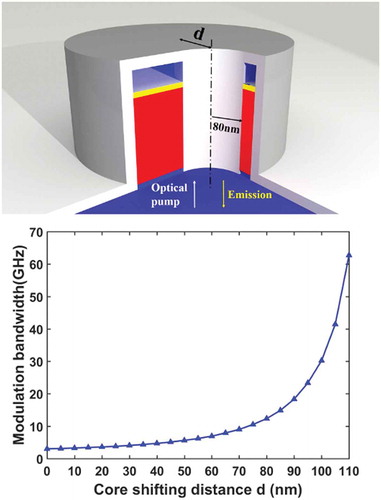
In 2018, an optically pumped shifted-core coaxial nano-emitter featuring small size, high modulation speed and high coupling efficiency to an adjacent waveguide was proposed [Citation24]. The device structure is shown in with 3D and cross-sectional views. The InGaAsP asymmetric-ring structure forms the body of the cavity, and the 10 nm InP layer on top of InGaAsP functions as a protection layer. The III-V semiconductor material is sandwiched between 40 nm SiO2 upper plug and 10 nm SiO2 lower plug. Therefore, the high refractive index contrast results in total internal reflection to form a Fabry–Pérot cavity in the vertical direction. Accompanied by the metal-dielectric-metal coaxial cavity in the horizontal direction, the optical mode is well confined in the nano-cavity with a footprint as small as 640 × 640 × 330 nm3 [Citation41]. Although InGaAsP’s wide gain spectrum from 1260 nm to 1590 nm poses a big challenge for the desired single-mode operation, the nano-cavity can be designed to support only the quasi-TEM mode within an impressively broad core shifting range from 0 to 110 nm. With single-mode operation, the spontaneous emission factor , defined as the ratio of spontaneous emission into the quasi-TEM mode to the total spontaneous emission, is close to unity. Therefore, high energy efficiency can be expected.
Figure 6. Structure of the shifted-core coaxial nano-emitter, reprinted from ref [Citation24] with permission. (a) 3D view. The SiO2/InGaAsP/InP/SiO2 stack forms a Fabry–Pérot cavity in the vertical direction. The Ag/InGaAsP/Ag structure forms a coaxial cavity in the horizontal direction. ‘d’ denotes core-shifting distance in the y direction. (b) Cross-sectional view.
![Figure 6. Structure of the shifted-core coaxial nano-emitter, reprinted from ref [Citation24] with permission. (a) 3D view. The SiO2/InGaAsP/InP/SiO2 stack forms a Fabry–Pérot cavity in the vertical direction. The Ag/InGaAsP/Ag structure forms a coaxial cavity in the horizontal direction. ‘d’ denotes core-shifting distance in the y direction. (b) Cross-sectional view.](/cms/asset/b258aa9b-dd3f-454b-9932-8388f73713f3/tapx_a_1658541_f0006_oc.jpg)
2.2.2 Numerical simulation: size, speed and emission directionality
The factor, resonant wavelength and modulation bandwidth of the device as a function of the core-shifting distance d are depicted in , showing that the modulation bandwidth can be greatly enhanced by the Purcell effect and reaches tens of GHz, which is well above the modulation speed of conventional LEDs.
Figure 7. (a) Q factor and resonant wavelength of the device as a function of the core-shifting distance. Inset: mode profile without shift (d = 0 nm) and at maximum shift (d = 110 nm). (b) Modulation bandwidth as a function of the core-shifting distance, reprinted from ref [Citation24] with permission. Note that the Q factor, Veff, Purcell factor and modulation bandwidth are all functions of the core shifting distance d.
![Figure 7. (a) Q factor and resonant wavelength of the device as a function of the core-shifting distance. Inset: mode profile without shift (d = 0 nm) and at maximum shift (d = 110 nm). (b) Modulation bandwidth as a function of the core-shifting distance, reprinted from ref [Citation24] with permission. Note that the Q factor, Veff, Purcell factor and modulation bandwidth are all functions of the core shifting distance d.](/cms/asset/c1ae19c3-d5b7-4930-85f3-4743a204b9a9/tapx_a_1658541_f0007_oc.jpg)
In addition to the small footprint and large modulation bandwidth, the shifted-core coaxial nano-emitter also emits directionally. The coupling efficiency between an optical cavity and a waveguide depends primarily on two factors: (a) the spatial overlap between the evanescent modes of the cavity and the adjacent waveguide; (b) k-vector matching between the two optical modes [Citation45]. Therefore, directional emission feature in this nano-emitter is desirable as it increases the coupling efficiency to waveguide. The 2D far-field analysis in shows that the omnidirectional emission in the un-shifted core case becomes bi-directional when the metallic core is shifted to one side of the cavity. The evolution of the far-field emission pattern and increased directivity in ) also demonstrate the same directional emission feature. Therefore, the coupling efficiency to an adjacent waveguide on chip is expected to increase because of the higher spatial optical mode overlap.
Figure 8. Far-field emission pattern of the shifted core coaxial nano-cavity, reprinted from ref [Citation24] with permission. (a) d = 0 nm; (b) d = 110 nm. Omni-directional emission can be changed to in-line bi-directional emission; (c) Evolution of emission directivity as a function of core-shifting distance.
![Figure 8. Far-field emission pattern of the shifted core coaxial nano-cavity, reprinted from ref [Citation24] with permission. (a) d = 0 nm; (b) d = 110 nm. Omni-directional emission can be changed to in-line bi-directional emission; (c) Evolution of emission directivity as a function of core-shifting distance.](/cms/asset/815af9dc-ea14-41bc-8fd8-21555e0f75c0/tapx_a_1658541_f0008_oc.jpg)
2.2.3 Rate-equation analysis for high speed and low power operation
The output power of nanoLEDs can be calculated according to ref [Citation6]:
where is the quantum efficiency,
is the total cavity mode loss rate, and
is the photon number. The distinct linear response for the photon number occurs in the limit of very low and very high pump rates [Citation46].
where
= energy confinement factor
= spontaneous emission factor (
for the single-mode shifted-core coaxial nano-cavity)
= cavity-enhanced spontaneous emission rate,
(
is the Purcell factor,
is the natural spontaneous emission rate: ~3 × 10⁷ s−1 for InGaAsP)
= pumping rate in the case of ideal current injection,
= excited state population at transparency: ~1.25 × 10¹⁸ × Va for the InGaAsP cavity
= absorption rate due to the gain medium,
= threshold pumping rate (at the onset of gain clamping),
= excited state population when total gain is equal to total loss,
Taking for the shifted-core coaxial cavity, all spontaneous emission is channelled into one single mode. If we apply
to equation (5),
will reduce to
, and equation (4) and (5) will collapse into one expression:
Pout is then simplified to . The quantum efficiency η is calculated as
where the cavity quality factor is mainly determined by two loss terms, namely, radiation loss and metal loss, such that [Citation47]
can be estimated and separated from
by removing the imaginary part of the cavity metal permittivity in numerical simulations.
At each core-shifting distance, the threshold current is expressed as the product of electric charge and the threshold pumping rate
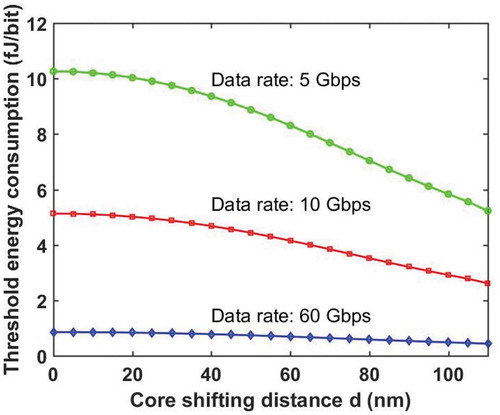
Although the design example of the shifted-core coaxial nano-emitter uses an optically pumped cavity and is thus not suitable for precise energy consumption calculation, we can still assume VDC = 3 V (a typical voltage level used in electronic ICs [Citation22]) to obtain a preliminary estimation. In this scenario, the estimated threshold energy consumption as a function of core-shifting distance can be computed. Modulation bandwidth based on small-signal analysis provides a good initial assessment of the modulation speed of lasers and LEDs, as proof of concept experiments are usually performed under this circumstance [Citation48]. However, large-signal digital modulation is used in practical applications. As a rule of thumb, the large-signal modulation rate is 1.3 times of its small-signal modulation bandwidth [Citation49,Citation50]. Because the modulation bandwidth of our device is able to reach 62 GHz, it should provide an open eye diagram as long as the data rate is lower than 80 Gbps. Dividing the threshold power consumption by data rate gives the threshold energy consumption [Citation51], as shown in . Note that all values are under the criteria of required energy consumption of 50 fJ/bit to be able to compete with electrical interconnects [Citation22]. An ideal current injection scenario is used in this evaluation, i.e. 100% conversion efficiency of electron-hole pairs into photons and 100% wall-plug efficiency are assumed. It can be seen that this shifted-core nano-emitter is very energy efficient within a large data rate range from 5 to 60 Gbps.
Figure 9. Threshold energy consumption at 3 V applied voltage, as a function of core-shifting distance.
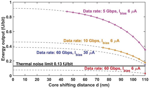
Assuming thermal detectors have 100% internal quantum efficiency, 1000 photons per bit are required for a sufficient signal-to-noise ratio above thermal detector noise [Citation52]. For an optical link operating at 1.55 μm (hω = 0.8eV), this corresponds to 0.13 fJ/bit, which sets the lower bound of the energy output per bit. For a conservative estimation, we use a 60 Gbps non-return-to-zero (NRZ) pseudorandom 27–1 bit sequence (PRBS) signal to modulate the input current, and show the energy output per bit for selected data rates and current levels in . Accompanied with the increasing core-shifting distance, higher operation speed can be reached ()). For each speed considered, we highlight the devices with the core-shifting distance range that can support the considered speed. If the device is used for on-chip telecommunication or quantum computation, the noise floor of the system is determined by the quantum shot noise. For optical communications, 20 photons/bit or 2.5 aJ/bit is thus needed to maintain a bit-error-rate of 10−9 [Citation7,Citation53]. Note that this device can operate at even higher data rates if the optical link has a lower noise floor.
Figure 10. Energy output/bit for selected data rates and current levels.
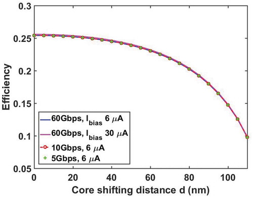
At a given bias current level and data rate, the device energy efficiency can be calculated by dividing the energy output by the energy consumption (). Several observations can be made:
Energy efficiency is independent of data rate, because both the energy output and energy consumption are expressed in terms of fJ/bit. The data rate is therefore canceled in the division.
Energy efficiency is lower for larger core-shifting distances. This is due to the reduction of the output power
, which results from the redshift of emission wavelength ()) and the decrease of quantum efficiency η (metal loss becomes more dominant) with increasing core shifting distance.
The energy efficiency at 30 μA bias current is slightly higher than that at 6 μA, although the difference is negligible.
Because we have assumed 100% conversion efficiency of electron-hole pairs into photons and 100% wall-plug efficiency at VDC = 3 V in calculating the energy consumption, the evaluated energy efficiency is expected to be significantly higher than experimentally achievable values. The wall-plug efficiency has not been studied in nanolasers to date, but wall-plug efficiency of 1.25 × 10⁻⁷ has been reported for electrically driven subwavelength optical nano-circuits [Citation27].
Figure 11. Device energy efficiency for selected data rates and current bias levels, as a function of core-shifting distance.
So far, the demonstration of the shifted-core coaxial nano-emitter has been limited to optically pumped devices only. In order to enable the more realistic electrically pumped operation, the semiconductor stack must be modified to incorporate a p-i-n junction consisting of doped InP carrier transport layers. In addition, an electrical isolation layer has to be incorporated to separate the gain material from the inner and outer metal claddings. Therefore, in the electrically pumped devices, the optical modes are less confined due to the inclusion of the high-index carrier transport layers, and consequently, both the factor and the
factor are lowered. Nonetheless, the cavity geometry and material stack can be adjusted to minimize the number of undesired modes, either by shifting these modes out of the spectral window of gain or by shrinking the device size, such that the cut-off free quasi-TEM mode is the only supported mode. These efforts will result in large
and Purcell factors simultaneously, and therefore a large modulation bandwidth. Moreover, it is also worth to consider utilizing photonic modes. The advantage of photonic modes is that they generally have higher
factors than plasmonic modes, and they are less affected by the inserted electrical isolation layer in a cavity designed for electrical pumping. The disadvantage of photonic modes is that the associated
factor has a maximum value of 0.5 as these modes typically appear in degenerate pairs, and that the Purcell factor tends to be lower than their plasmonic counterparts due to their larger effective modal volume. In addition, current crowding and the associated excessive heat generation, as are common in nanoscale devices, also need to be managed for power-efficient operation. If all of the above problems can be properly addressed, an electrically pumped nanoLED of this type can be expected to play an important role in the future high-speed optical communication systems.
3. Discussion and future work
In this review, recent developments of nanoscale light sources for on-chip optical communications are revisited. We first discussed the feasibility of nanoLEDs being the light source for short-range optical link; then we selectively chose size scaling and enhanced spontaneous emission of nanoLEDs as the main topics of this short review. Benefits and disadvantages of device downscaling were discussed, and we used antenna theory and Purcell effect to explain the enhancement of spontaneous emission in metallic nano-cavities. Lastly, we illustrated our points with a high Purcell factor shifted-core coaxial nano-emitter design example [Citation24]. By using rate equations to evaluate its frequency response and energy consumption, the device performance is verified to fulfill the need of high speed and energy-efficient nanoscale light sources.
Despite the growing interest in nanoLED designs, there are still plenty of challenges from the fabrication and application aspects before nanoLEDs’ practical insertion into chip-scale circuits: (1) non-radiative surface recombination: although surface passivation has been demonstrated as an effective method to reduce the surface recombination, process compatibility and long-term stability of such method have not yet been well studied; (2) low optical coupling to adjacent components such as waveguides: because of the low mode overlap and large k-vector mismatch, the coupling efficiency is not satisfactory; (3) reliability: high power density raises reliability issues such as device self-heating and electro-migration; (4) output power and energy efficiency. Nevertheless, nanoLED is becoming a very attractive light source candidate for high-speed short-range optical interconnects.
Disclosure statement
No potential conflict of interest was reported by the authors.
Additional information
Funding
References
- Cisco. Cisco global cloud index : forecast and methodology, 2016–2021. Cisco. 2018.
- Miller DAB. Rationale and challenges for optical interconnects to electronic chips. Proc IEEE. 2000;88:761–779.
- Sun C, Wade MT, Lee Y, et al. Single-chip microprocessor that communicates directly using light. Nature. 2015.
- Goodman JW, Leonberger FI, Kung SY, et al. Optical interconnections for VLSI systems. Proc IEEE. 1984;72:850–866.
- Astfalk G. Why optical data communications and why now? Appl Phys A. 2009;95:933–940.
- Coldren LA, Corzine SW. Diode Lasers and Photonic Integrated Circuits. John Wiley and Sons, Hoboken, NJ. 2012.
- Li N, Han K, Sorger V, et al. Nanoscale light sources for optical interconnects. J Lasers Opt Photonics. 2017;04:3–5.
- Dolores-Calzadilla V, Romeira B, Pagliano F, et al. Waveguide-coupled nanopillar metal-cavity light-emitting diodes on silicon. Nat Commun. 2017;8:1–8.
- Wheeler HA. Fundamental limitations of small antennas. Proc IRE. 1947;35:1479–1484.147148
- Eggleston MS, Messer K, Zhang L, et al. Optical antenna enhanced spontaneous emission. Proc Natl Acad Sci. 2015.
- Purcell EM. Spontaneous Emission Probabliities at Radio Frquencies. Phys Rev. 1946;69:674.
- Lau EK, Lakhani A, Tucker RS, et al. Enhanced modulation bandwidth of nanocavity light emitting devices. Opt Express. 2009;17:7790.
- Tucker RS. High-speed modulation of semiconductor lasers. J Light Technol. 1985;3:1180–1192.
- Zhu NH, Shi Z, Zhang ZK, et al. Directly modulated semiconductor lasers. IEEE J Sel Top Quantum Electron. 2018.
- Ning C-Z. Semiconductor nanolasers and the size-energy-efficiency challenge: a review. Adv Photonics. 2019;1:014002.
- Baba T, Fujita M, Sakai A, et al. Lasing characteristics of GaInAsP-InP strained quantum-well microdisk injection lasers with diameter of 2-10 µm. IEEE Photonics Technol Lett. 1997;9:878–880.
- Seo MK, Jeong KY, Yang JK, et al. Low threshold current single-cell hexapole mode photonic crystal laser. Appl Phys Lett. 2007;90.
- Oulton RF, Sorger VJ, Zentgraf T, et al. Plasmon lasers at deep subwavelength scale. Nature. 2009.
- Noginov MA, Zhu G, Belgrave AM, et al. Demonstration of a spaser-based nanolaser. Nature. 2009.
- Hill MT, Gather MC. Advances in small lasers. Nat Photonics. 2014.
- Hayenga WE, Garcia-Gracia H, Hodaei H, et al. Metallic coaxial nanolasers, Adv Phys X. 2016;1:262–275.
- Ni C-YA, Chuang SL. Theory of high-speed nanolasers and nanoLEDs. Opt Express. 2012;20:16450.
- Fortuna SA, Taghizadeh A, Yablonovitch E, et al., “Toward 100 GHz direct modulation rate of antenna coupled nanoLED,” In 2016 IEEE Photonics Conference, IPC 2016, Waikoloa, HI. IEEE; 2017. pp. 216–217.
- Li X, Gu Q. Ultrafast shifted-core coaxial nano-emitter. Opt Express. 2018;26:15177–15185.
- Fiore A, Chen JX, Ilegems M. Scaling quantum-dot light-emitting diodes to submicrometer sizes. Appl Phys Lett. 2002;81:1756–1758.
- Shambat G, Ellis B, Majumdar A, et al. Ultrafast direct modulation of a single-mode photonic crystal nanocavity light-emitting diode. Nat Commun. 2011;2:4–5.
- Huang KCY, Seo MK, Sarmiento T, et al. Electrically driven subwavelength optical nanocircuits. Nat Photonics. 2014;8:244–249.
- Vesseur EJR, De Abajo FJG, Polman A. Broadband Purcell enhancement in plasmonic ring cavities. Phys Rev B - Condens Matter Mater Phys. 2010.
- Kuttge M, García De Abajo FJ, Polman A. Ultrasmall mode volume plasmonic nanodisk resonators. Nano Lett. 2010.
- Kinkhabwala A, Yu Z, Fan S, et al. Large single-molecule fluorescence enhancements produced by a bowtie nanoantenna. Nat Photonics. 2009;3:654–657.
- Arbel D, Berkovitch N, Nevet A, et al. Light emission rate enhancement from InP MQW by plasmon nano-antenna arrays. Opt Express. 2011;19:9807.
- Agrawal GP, Dutta NK. Semiconductor lasers. Springer US, Boston, MA; 1993.
- Ma RM, Oulton RF. Applications of nanolasers. Nat Nanotechnol. 2019.
- Hall RN. Coherent light emission from p-n junctions. Solid State Electron. 1963;6:405–408.
- Holonyak N, Bevacqua SF. Coherent (visible) light emission from Ga(As1-xPx) junctions. Appl Phys Lett. 1962.
- Casey HC, Stern F. Concentration-dependent absorption and spontaneous emission of heavily doped GaAs. J Appl Phys. 1976;47:631–643.
- Ieee J, Electronics Q. Power and modulation bandwidth of GaAs-AIGaAs high-radiance LED‘s. Quantum. 1978;14:150–159.
- Feng M, Holonyak N, Hafez W. Light-emitting transistor: light emission from InGaP/GaAs heterojunction bipolar transistors. Appl Phys Lett. 2004;84:151–153.
- Walter G, Wu CH, Then HW, et al. Tilted-charge high speed (7 GHz) light emitting diode. Appl Phys Lett. 2009;94:1–4.
- Miura R, Imamura S, Ohta R, et al. Ultralow mode-volume photonic crystal nanobeam cavities for high-efficiency coupling to individual carbon nanotube emitters. Nat Commun. 2014.
- Khajavikhan M, Simic A, Katz M, et al. Thresholdless nanoscale coaxial lasers. Nature. 2012;482:204–207.
- Maksymov IS, Besbes M, Hugonin JP, et al. Metal-coated nanocylinder cavity for broadband nonclassical light emission. Phys Rev Lett. 2010.
- Roelkens G, Karouta F, van der Tol J, et al. Photonic integration in indium-phosphide membranes on silicon. IET Optoelectron. 2011;5:218–225.
- Peucheret C. Direct and external modulation of light. Direct. 2006.
- Debnath K, Welna K, Ferrera M, et al. Highly efficient optical filter based on vertically coupled photonic crystal cavity and bus waveguide. Opt Lett. 2013.
- Ma RM, Oulton RF, Sorger VJ, et al. Plasmon lasers: coherent light source at molecular scales. Laser Photonics Rev. 2013;7:1–21.
- Kai T, Mei-yu W, Fu-cheng W, et al. The two-dimensional hybrid surface plasma micro-cavity. J Mod Opt. 2018;65:1595–1600.
- Ding K, Diaz JO, Bimberg D, et al. Modulation bandwidth and energy efficiency of metallic cavity semiconductor nanolasers with inclusion of noise effects. Laser Photonics Rev. 2015;9:488–497.
- Tucker RS, Wiesenfeld JM, Downey PM, et al. Propagation delays and transition times in pulse-modulated semiconductor lasers. Appl Phys Lett. 1986;48:1707–1709.
- Takeda K, Sato T, Shinya A, et al. Few-fJ/bit data transmissions using directly modulated lambda-scale embedded active region photonic-crystal lasers. Nat Photonics. 2013;7:569–575.
- Yang Y-D, Zhang Y, Huang Y-Z, et al. Direct-modulated waveguide-coupled microspiral disk lasers with spatially selective injection for on-chip optical interconnects. Opt Express. 2014;22:824.
- Agrawal GP. Fiber-optic communication systems, 4th ed. John Wiley and Sons, New York, NY. 2011. p. 1–600.
- Romeira B, Fiore A. Physical limits of nanoLEDs and nanolasers for optical communications. Proc IEEE. 2019;1–14.