
 ?Mathematical formulae have been encoded as MathML and are displayed in this HTML version using MathJax in order to improve their display. Uncheck the box to turn MathJax off. This feature requires Javascript. Click on a formula to zoom.
ABSTRACT
Scales in the 100 nm range represent a generic cornerstone for laser material processing, enabling novel size-dependent functions on surfaces and in the bulk and thus a new range of technological applications. On these scales, the processed material acquires optical, transport or contact properties that do not only rely on local effects on singular topographic features but involve increasingly collective behaviors. Rapid access to sub-100 nm features with intense coherent light represents nevertheless a challenge in laser structuring in view of the optical diffraction limit. Ultrafast non-diffractive beams with controllable time envelopes can overcome this limit and achieve super-resolved processing, a prerequisite for the next generation of flexible and precise material processing tools. They show a remarkable capacity of structuring transparent materials with high degree of accuracy and exceptional aspect ratio. This capacity relies on triggering fast hydrodynamic and material fracture effects with characteristic spatial scales in the nm range. Reviewing the present achievements and technical potential, we discuss from a dynamic viewpoint the physical mechanisms enabling structural features beyond diffraction limit achieved using ultrafast Bessel beams and indicate applications of high technical relevance.
Abbreviations: PCM: phase contrast microscopy; SEM: scanning electron microscopy; NBOHC: non-bridging oxygen hole center
PACS CLASSIFICATION:
1. Introduction
Material structuring represents today the pillar for a range of rapidly growing application areas in emerging technologies. Ultrafast laser techniques hold in this context unique advantages as rapid, flexible, non-contact processing tools, providing at the same time on-target intensities in the TW/cm range, sufficient to structure any material, even the hardest ones. Their employment in technological processes is fueled by strong developments in terms of average and peak power, feedthrough, and digital manufacturing capability [Citation1].
The question of resolution is crucial for further industrial insertion and a lot of interest is devoted to the capacity of reaching the nanoscale [Citation2–Citation4]. The scale of structuring, the minimal feature size, and the resulting morphologies and topographies define then the function that can be attached to the structured material. This function pertains to optical, mechanical, or contact properties of the processed materials, upgrading the relevant performance; optical efficiency, mechanical strength, or contact atributes. Achieving high processing resolution and minimal feature size requires an interdisciplinary effort in engineering optical and material effects. Rapid access to scales below 100 nm in two and three dimensions would then enable unprecedented design capabilities for materials and functions, being thus one major thrust of future developments in laser processing technologies.
A first advantage of ultrashort laser pulses for precise manufacturing lies in their short duration, below s. Thus the modification process speeds up before significant energy diffuses in the material (diffusion length being
with
thermal diffusivity and
the characteristic process time), restricting thus the interaction to its optical borders. It thus harnesses the benefit of the high on-target intensities. The optical resolution provided by the performance of beam delivery determines in principle the processing scale.
Structuring material using optical beams suffers nevertheless from focusing restrictions related to diffraction [Citation5]. Inherent to focusing a light wave through an optical element of finite numerical aperture, optical diffraction imposes limitations to the minimal achievable size of the focusing spot. For a uniformly illuminated diffraction-limited optical system giving an Airy spot at the focus, its radius at the zero intensity point is , with
being the wavelength and
the numerical aperture. Correction factors can be applied for truncation ratios and pupil illumination patterns. For the typical laser processing wavelengths in the near-infrared and the usual beam delivery optics of moderate numerical apertures, the resulting beam spot size lies in the 1 µm range. For the highest NAs used to obtain the smallest spots the size becomes comparable to the half-wavelength, with the beam rapidly diverging after reaching the focal point. This limitation was early recognized and attempts to achieve processing resolutions beyond diffraction limit have accompanied ultrafast laser techniques almost from their first use in material processing. These attempts were based on engineering the focal spot or on the exploitation of the propagation behavior.
The development made equally use of several intrinsic features of ultrafast laser ablation; deterministic character, nonlinear interaction, the use of evanescent coupling, reduced heat diffusion, the existence of a material ablation threshold, and the process of self-organization. Deterministic interaction with light implies in this context that in various materials, notably in dielectrics, the optical radiation generates itself the absorption centers and does not rely on extrinsic, statistically-distributed factors to deposit energy (e.g. impurities and pre-existing structural defects). This is more pronounced for wide band-gap materials where several photons absorbed instantaneously are required to bridge the energy gap, initiating further absorption on thus-generated free carriers. Here the high intensity of focused ultrashort beams ensures sufficient density of photons to achieve direct nonlinear excitation. The nonlinear character of absorption suggests that a spatially-varying beam profile seen by the material is a power function of the incident beam profile and becomes thus narrower. This pertains particularly to Gaussian spatial distributions of the electric field
, the standard output of a commercial ultrafast laser system. Within a multiphoton ionization process, the absorption profile matches approximately
, with
being the number of photons required to be absorbed by a valence band electron transiting to the conduction band; the transition probability being proportional to the photon density. These observations were facilitated by interactions at surfaces using Gaussian beams, showing material effects depending on the local intensity values. Gentle and strong ablation phases were observed on dielectric surfaces and explained by the weight of a nonlinearily narrowed absorption profile at the interface [Citation6].
Relying on the deterministic character of the ultrafast laser interaction with gap materials which minimizes fluctuations in energy deposition, Joglekar et al. [Citation7] used accurate control of the beam energy with respect to a deterministic material ablation threshold and created the conditions that just the tip of the Gaussian distribution exceeds the threshold. Ablation occurs in the restricted zone over the threshold. Thus they demonstrated a remarkable below 100 nm nanomorphing capacity. A similar fine tune of energy was used by Korte et al [Citation8]. to achieve nanostructuring of metals, recognizing through thermionic emission an intensity dependent non-equilibrium energy deposition even for non-gap materials. Using shorter wavelengths and interference techniques, Klein-Wiele et al. [Citation9] extrapolated the threshold-based nanostructuring method to large scale patterning, achieving large nanopatterned surfaces. The capability to reach sub-wavelength resolution can further benefit from engineering the far-field optical fields using advanced designs of the optical elements and irradiation, often inspired from microscopy [Citation10,Citation11].
Further downsizing in processing scales originates from the use of near-field waves. Albeit a slowdown in process speed, a straightforward method to overcome diffraction limit was seen in processing using optical evanescent fields from the tip of an optical fiber [Citation12] or microscope probes [Citation13,Citation14] in a scanning near-field microscopy approach. The possibility to work in the near-field was extrapolated to the use of microspheres self-organized on surfaces [Citation15,Citation16], a way to equally parallelize the interaction.
At the same time, the nonlinearity of interaction is an effective way of adjusting irradiation profiles. Taking advantage of the nonlinear character of absorption that squeezes the energy deposition profile, White et al. [Citation17] demonstrated high aspect ratio nanoscale processing on dielectric surfaces. The nonlinearity of interaction offers a far wider range of adjusting laser parameters to achieve energy confinement. A highly efficient way of surface nanostructuring harnessing the physics of interaction was archived using temporal beam engineering. Employing temporally asymmetric pulses (e.g. Airy pulses), Englert et al. [Citation18] was able to steer the sequence of multiphoton and collisional ionization within the spot, generating the highest ionization efficiency at the apex. This type of excitation spatio-temporal control triggers nanoscale ablation with record sizes for the processed features.
The concept can be extrapolated for volume interactions, where nonlinear propagation takes a leading place in establishing local intensity profiles. Whenever a dielectric medium is concerned, self-focusing of laser beams can confine the energy on scales smaller than the standard focusing capability.
In parallel to direct focusing approaches, a different concept emerged for surface and bulk nanostructuring; the self-organization of periodic patterns (see for example Ref [Citation19,Citation20]. and the references therein) on excited materials. They reflect a capacity of mutual influence between material and optical landscapes resulting from scattering, the emergence of surface waves or the self-organization capacity of hydrodynamic instabilities [Citation19,Citation21]. Even though they were reported half a century ago [Citation22], the onset of regular topography patterns with coherent light is a spectacular effect that keeps attracting interest as structured surfaces and volumes acquire novel properties ranging from biomimetic functions [Citation23], non-plasmonic coloring [Citation24], or contact characteristics [Citation25], to anisotropic optical functions [Citation26], microfluidic transport properties [Citation27], or data storage capacity [Citation28]. Strong corrugation renders equally interesting absorption properties on surfaces based on light trapping [Citation29,Citation30], with interest in infrared detection and enhanced photovoltaic effects. The interaction of coherent radiation with surfaces and volumes presenting extrinsic or radiation-induced scattering centers (for example roughness) will develop in-phase scattered waves with evanescent components. Through interference, wavelength and polarization-dependent standing wave patters will form, imprinting their fingerprints in the material [Citation31]. The emerging topographies will enhance and rearrange scattering events in near and far-field, inducing with each incoming pulse order in the matter organization process at different periodicities and orientations. Periodic patterns with subwavelength periodicities will form assisted by the feedback between light and matter.
All these demonstrations recognized a straightforward physical reality; the achievable structuring size on the nanoscale should rely on a specific material response to laser radiation. Being a material reaction, it will therefore not experience an optical limit, but a material organization limit which, for a large range of material phenomena, lies one order of magnitude below. Typical examples are hydrodynamic and fracture effects, which have a characteristic scale of with
being the speed of sound and
the characteristic time (i.e. the elapsed time of the process), usually in the ps and ns range [Citation32]. Achieving extreme size control in laser material interaction will require beams that can steer and adapt to material reaction. Concepts of smart beam engineering have already emerged [Citation33] based on driving with light (and energy deposition rate) specific thermal and mechanical material reactions.
Recently, a new class of optical beams emerged for processing applications [Citation34–Citation40] in hard and soft matter; the non-diffractive beams, and, within this class, notably the zero-order Bessel-Gauss beams (called hereafter Bessel beams for simplicity) [Citation41–Citation45]. These beams exhibiting a central spot resistant to diffraction reflect a particular longitudinal geometry of quasi-constant intensity and with a transverse profile given by a Bessel function . The field can be expressed as
, where
are the longitudinal and radial wavevectors, and
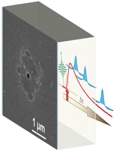
the radius. A schematic representation of a Bessel beam is given in ) and a processing example employing this kind of beams is depicted in ). Their principal characteristic is that they can keep a narrow beam size as they evolve in space without spreading out, and have the capacity to regenerate as they encounter obstacles. This review will discuss the mechanisms and the advantages of using non-diffractive Bessel beams for ultrafast laser material processing.
Figure 1. (a) Schematic description of zero-order Bessel beams. The figure shows the conical refraction of the incoming front and the emergence of the interference pattern with the axial core and the annular features characteristic to Bessel beams. (b) Conceptual image of surface and bulk processing with Bessel pulses [Citation46]. Left: input surface pattern generated by a singe shot tightly focused ultrashort (60 fs, 14 µJ) Bessel beam () on fused silica surface; scanning electron microscope (SEM) image. The Bessel ring pattern is recognizable. Right: Back surface (exit surface) nanoscale structure in fused silica induced by a single shot moderately-focused ps stretched laser pulse (5 ps, 14 µJ,
); SEM image. (c) Example of sub-100 nm structures achieved by tightly focused Bessel beams in volume glasses [Citation46]. Transverse morphology features involving direct volume focusing of ultrafast (60 fs) Bessel beams of higher angle (
).
![Figure 1. (a) Schematic description of zero-order Bessel beams. The figure shows the conical refraction of the incoming front and the emergence of the interference pattern with the axial core and the annular features characteristic to Bessel beams. (b) Conceptual image of surface and bulk processing with Bessel pulses [Citation46]. Left: input surface pattern generated by a singe shot tightly focused ultrashort (60 fs, 14 µJ) Bessel beam (θair=22∘) on fused silica surface; scanning electron microscope (SEM) image. The Bessel ring pattern is recognizable. Right: Back surface (exit surface) nanoscale structure in fused silica induced by a single shot moderately-focused ps stretched laser pulse (5 ps, 14 µJ, θglass≃8∘); SEM image. (c) Example of sub-100 nm structures achieved by tightly focused Bessel beams in volume glasses [Citation46]. Transverse morphology features involving direct volume focusing of ultrafast (60 fs) Bessel beams of higher angle (θglass≃15∘).](/cms/asset/4ea16d95-af00-4693-8456-44e83969fb83/tapx_a_1659180_f0001_oc.jpg)
The advantage of these beams for laser processing applications is manifold: (1) the high aspect ratio enabling large scale structuring, (2) their intrinsic nonlinear stability as they don’t propagate longitudinally as their Gauss counterparts do, (3) the potentially strong energy confinement, and (4) the lateral relaxation flow. A conceptual example of Bessel beam interaction with a dielectric material is shown in , where the figure describes surface and bulk interaction. It is to be noted that the ring pattern is observable on the input surface but not on the exit part. ) indicates the cross-section of a sub-100 nm feature achieved by tight focusing of Bessel beams of sub-100 fs duration [Citation46].
2. Bessel–Gauss beams
It is first of interest to briefly indicate the main geometrical features and the practical concepts for generating Bessel beams. Generated experimentally by Durnin et al. [Citation41] as beams with a central spot that does not diverge over a long distance, zero-order Bessel beams develop an extended core of light surrounded by an ensambles of rings [Citation42]. Various optical setups can be used for generation (see for a review Ref [Citation47,Citation48]. and references therein). They rely on conical intersection of wavefronts generated by either a conical phase (via axicon, spatial light modulator) and subsequent refraction or diffraction, or by the convergence of annular beams with non-varying polarization. Among them the use of axicon is most common [Citation43]; an optical element that imposes a conical phase, as being energetically efficient for creating the non-diffractive pattern. Particularly the axicon, a conical prism element, was early recognized for its capability of forming line focus, relaxing the alignement conditions in imaging optical systems [Citation43]. Upon refraction on the optical cone, a standing interference pattern is formed along the propagation axis ()), giving the elongated profile. The main core and the rings reflect successive interference orders of the incoming wavefronts. In this conical geometry the circular rings serve as an energy reservoir for replenishing the core, rendering a remarkable stability to the beam, for example when encountering obstacles. Being a projection of the initial beam transverse dimensions and more precisely the geometrical places where the converging wavefronts cross and superpose on the propagation axis, the core can extend significantly over the Rayleigh range of Gaussian beams focused in similar conditions. The longitudinal extension depends on the convergence angle and the lateral size of the input beam . High aspect ratios can be obtained (
). The longitudinal elongation
and the diameter
of the core are defined by the conical angle
(
,
, with
being the wavevector). For
and a wavelength
= 800 nm, the
goes in the sub-micrometer range. The axial profile can be controlled using apodizing techniques [Citation49,Citation50] and uniform distributions can be achieved by spectral filtering the leakage from non-ideal axicon tips [Citation51]. The as-generated beam can be demagnified and re-imaged to the workpiece by relay optics [Citation51], with micron-sized cores and aspect ratios exceeds easily a factor 100 in processing conditions. Multi-axicon setup was recently used to obtain record aspect ratios over 10,000 [Citation52].
3. Technological applications of non-diffractive ultrafast bessel-Gauss laser beams
Known mostly for applications in optical trapping and manipulation, imaging and nonlinear optics (see Ref [Citation47]. and the references therein), the Bessel beams have recently developed a specific interest in laser material structuring and fabrication in view of their particular characteristics, notably geometrical aspect and non-diffractive feature. They can be first used to manipulate light optical elements on surfaces, driving optical interactions between the object and the interfaces. Bessel beam trapping and steering of microspheres near surfaces was thus used for near-field subwavelength nanopatterning [Citation53]. They can equally be used for direct write of ablative features in the bulk and on surfaces [Citation54] or through drilling in transparent materials [Citation55]. To grasp the essential features of non-diffractive beams in material processing, we will briefly point out several cases of using Bessel beams for high impact applications [Citation40,Citation56–Citation62], that are finding now their way into industrial-grade processes. These were recently reviewed in Ref [Citation63].
The remarkable characteristics of Bessel beams in terms of aspect ratio have made them attractive for large scale processing applications. Given the one-dimensional geometry of interaction, the relaxation of energy and the resulting material constraints occur radially, along the direction of the highest gradients, creating thus transverse forces of significant strengths. These features, and the resulting forces and stresses, are of interest when separation of matter is concerned and are thus becoming essential in large scale high–speed cutting and cleaving applications [Citation57,Citation58,Citation64]. An example of glass cleaving operation [Citation57] is given in ), emphasizing the scale and the quality of material separation. In view of its optical and mechanical properties glass is a material of strong technical relevance for displays in consumer electronics or for medical devices, and glass cleaving and cutting operations have a clear market potential. Non-diffractive beams are particularly suited for glass (or in general dielectrics) separation technologies, as they can introduce hidden in-volume modifications (stealth machining) with large aspect ratios and stress fields orientations that facilitate separation [Citation64]. In addition, creating asymmetries in the beam profile (e.g. ellipticity, tilted fronts, or specific polarization [Citation40,Citation64] relative to material crystalline axes for crystalline dielectrics) can orient the resulting stress field to achieve maximum effect. This weakens the bonding strength on specific directions and leads to efficient separation with non-diffractive high aspect ratio beams that present asymmetric elongations along the transverse direction. ) shows the example of oriented fracture lines creating a continuous fracture plane and driving the separation process with a resulting high quality of the separation wall [Citation58]. Various concepts of non-diffractive asymmetric beam engineering in forms of ‘optical knives’ and ‘optical shovels’ were recently reviewed by Orlov et al. [Citation65].
Figure 2. (a) Examples of glass parts cleaved and cut by non-diffractive Bessel beams. (b) Images of resulting surface and side walls (courtesy of K. Mishchik, Amplitude Systems [Citation57]). (c) A Bragg gratings waveguide fabricated by a combination of Gauss and Bessel beam irradiation [Citation70]. The figure shows the transmitted mode (d). An electron microscopy image of the nanostructured range is given (e). (f) Resonant Bragg optical transmission spectrum in the telecom range. (g) Examples of embedded waveguides with Bessel nano-scatterers sampling electric fields for reconstructing spectral information [Citation71].
![Figure 2. (a) Examples of glass parts cleaved and cut by non-diffractive Bessel beams. (b) Images of resulting surface and side walls (courtesy of K. Mishchik, Amplitude Systems [Citation57]). (c) A Bragg gratings waveguide fabricated by a combination of Gauss and Bessel beam irradiation [Citation70]. The figure shows the transmitted mode (d). An electron microscopy image of the nanostructured range is given (e). (f) Resonant Bragg optical transmission spectrum in the telecom range. (g) Examples of embedded waveguides with Bessel nano-scatterers sampling electric fields for reconstructing spectral information [Citation71].](/cms/asset/f577a16d-b70a-47e0-a9f1-5c360c7861b7/tapx_a_1659180_f0002_oc.jpg)
A second feature of interest derives equally from the non-diffractive character, with a characteristic beam length outpacing the confocal length of a similarly focused Gauss beam. A high tolerance to focusing with respect to the workpiece is becoming of interest, particularly for high precision applications where the use of rapidly diverging tightly focused Gauss beams becomes difficult. This implies that the energy can be brought to the point of impact by non-diffractive beams without involving accurate focusing and positioning, particularly when complex topographies and non-planar surfaces are involved. A recent example in Ref [Citation60]. demonstrated joining and welding of glass materials with joining strengths up to 16.5 MPa using Bessel beams as carriers of energy at the interface. Several laser and equipment producers are integrating now joining and cutting technologies with non-diffractive beams in industrial processes.
The self-regeneration of Bessel beams as the rings continuously feed the core with energy is of interest when the processing environments suffer from the presence of debris and particulates as it is the case in deep-drilling applications. Being able to penetrate materials and reform in drilled channels, they may ensure a maximum efficiency in through-drilling of materials, including non-transparent ones [Citation66,Citation67]. For drilling applications requiring specific forms, the aspect ratio can be tailored using phase/amplitude corrections and core-ring contrast can be adjusted on the expense of the non-diffractive length [Citation50,Citation68].
Last but not the least, the feature that will be the base of the following discussion is the capability of achieving light confinement and structuring on the nanoscale in bulk materials. Bessel beams are particularly suited for this task and early applications span a range of fields from polymer processing [Citation38] to optical transfection of cells [Citation39]. We have indicated above that non-diffractive beams can potentially determine a material response that can bypass optical limits and achieve structural features not limited by optical resolution. ) indicated that record processing resolutions below 100 nm can be attained. The 100 nm scale represents a cornerstone in laser processing as the processed functions depend not only on local topographies but on the onset of collective effects. This feature size is of interest in transport phenomena, affecting for example phonon scattering on nanostructured surfaces and volumes, laying down the possibility to control energy exchange. Extrapolated to optical domains, this is specifically important in applications requiring the definition of sharp optical resonances and sub-wavelength sampling of optical signals in embedded optical systems. If Bessel laser photoinscription of integrated optical elements was demonstrated in the form of waveguides [Citation35] or gratings [Citation56,Citation69], hybrid systems combining micro and nanosized features offer extended opportunities not only for transporting and routing the optical fields but also for sampling the optical signals, accessing thus the information within. This function can be achieved with periodic nanoscale modulation of the refractive index inside an optical waveguide determining a highly efficient Bragg optical resonance [Citation70] or by inserting nanoscale non-perturbative scattering centers that can sample the field, read it, and reconstruct the spectral information [Citation71,Citation72]. The example below discusses the possibility of sampling and manipulating optical fields in integrated optical systems. shows an example of Bragg gratings waveguide photoinscribed using non-diffractive beams with a high Bragg resonance of 4 dB/mm in the transmission spectrum around 1.5 µm in the telecom band [Citation70]. Similarly, ) gives examples of embedded optical systems in chalcogenide glasses functioning as infrared spectrometers where Bessel generated nano-scatterers can efficiently interact with the mode and sample the electric field, reconstructing thus spectral information [Citation71].
The use of Bessel beams involve not only subtractive approaches but equally additive techniques. One example refers to two photon polymerization and three-dimensional generation of micro- and nanosized objects [Citation37]. Altogether, the use of Bessel beams can be of advantage in specific applications, despite their higher energetic costs to ensure the same fluence levels as the Gauss beams.
These applications and the accurate processing scales require introspection and comprehension of the physical mechanisms of excitation, transformation and structuring of matter using non-diffractive beams. We will discuss in the following physical aspects and material reactions leading to structuring sizes in the 100 nm range using infrared ultrafast Bessel laser beams propagating in bulk transparent materials. Volume interactions in fused silica glass will constitute the main case of study.
4. Fundamental mechanisms for machining with ultrafast non-diffractive Bessel–Gauss beams
4.1. Matter reorganization and refractive index modifications
The mechanisms of material transformation upon the incidence of ultrafast Bessel beams can be decomposed in two categories. A first class is represented by generic laser-induced processes, common between Gauss and Bessel beams, that rely on intensity-driven effects (e.g. ionization, relaxation of electronic energy). The second class is specific to the geometry of interaction for non-diffractive beams and includes nonlinear propagation features and aspect forms of material modification. We will shortly discuss below several propagation, excitation, and relaxation mechanisms that bear the signature of non-diffractive beams. The discussion will start from the observation that the interaction regime can be classified in two main types; a gentle interaction that generates structural but not hydrodynamic evolution and a strong interaction generating void-like one-dimensional structures that involve hydrodynamic activity and mass-displacement. This is best illustrated in in the case of irradiated fused silica. Here one can define a gentle interaction regime for generating positive index changes (denoted type I in )) and a strong interaction for void-like negative index-change domains (type II, )). These can take the form of uniform or modulated longitudinal negative index domains. The discussion below will emphasize the possible structural evolutions generated by laser irradiation, from ionization and bond-breaking to heating and hydrodynamic evolutions. These are generic changes that can describe the evolution of various dielectric materials under laser light. The resulting structures are mostly presented using optical phase contrast microscopy (PCM), where dark and bright zones represent amplitude-converted phase shifts originating from domains of increased and decreased refractive index respectively. If the examples pertain mostly to fused silica glass, general features can be extrapolated to large classes of glasses and crystals, notwithstanding material specificities in terms of organization of molecular network and thermomechanical properties.
Figure 3. Structuring regimes in bulk fused silica under Bessel ultrafast laser irradiation illustrated with phase contrast microscopy images. The relative refractive index scale is given, with black and white color meaning positive and negative index changes respectively, with respect to the initial refractive index value. (a) regime of positive refractive index change (type I) in ultrafast (60 fs) multipulse cumulative regimes for moderate focusing conditions (). (b) regimes of type II negative index change; uniform and fragmentation modes in single pulse regimes (
) for the achieved structures. To avoid intensity clamping, tight focusing or dispersion engineering can be used [Citation46,Citation92], employing respectively ultrashort and short pulses.
![Figure 3. Structuring regimes in bulk fused silica under Bessel ultrafast laser irradiation illustrated with phase contrast microscopy images. The relative refractive index scale is given, with black and white color meaning positive and negative index changes respectively, with respect to the initial refractive index value. (a) regime of positive refractive index change (type I) in ultrafast (60 fs) multipulse cumulative regimes for moderate focusing conditions (θglass≃8∘). (b) regimes of type II negative index change; uniform and fragmentation modes in single pulse regimes (θglass≃15∘) for the achieved structures. To avoid intensity clamping, tight focusing or dispersion engineering can be used [Citation46,Citation92], employing respectively ultrashort and short pulses.](/cms/asset/33aca29a-d0dd-4b32-a05c-bb03adc9ff33/tapx_a_1659180_f0003_oc.jpg)
4.2. Nonlinear propagation
The interaction between ultrafast beams and matter has a dominant nonlinear character, mixing propagation and ionization effects. The non-diffractive Bessel beams are nonlinearly stable [Citation73,Citation74], robust, as the core is continuously supplied with photons, and less affected by spherical aberrations. This is an essential difference between Gaussian and Bessel illumination that lies in the nonlinear propagation regime. While at ablation-level intensities (with corresponding peak powers above the critical power, typically in the MW range), Gaussian beams undergo strong Kerr self-focusing and plasma defocusing, resulting in a complex spatio-temporal reshaping, Bessel beams can sustain a more stable propagation-invariant regime [Citation75]. This imposes singular stable interaction conditions where the main nonlinear factors seem well balanced, notably Kerr nonlinearity, optical diffraction or carrier light defocusing. Stability means in this context a uniform energy deposition region while preserving the range of propagation with a constant transverse spread; i.e. constant waist. We recall that Kerr-induced nonlinear phase distortions cumulate with the propagation distance. The nonlinear stability is a consequence of transverse characteristics () which remain smaller than the micron-sized nonlinear propagation length
for typical ultrashort exposures, with
being the nonlinear refractive index and
the peak intensity [Citation74].
4.3. Ionization and energy deposition
Consequences of the interplay between nonlinear propagation and ionization are readily observed in the interaction with the transparent matter. The swift excitation via field ionization, multiphoton absorption, and collisional ionization creates a carrier plasma in the material. Primary excitation relies on multiphoton, tunnel, and above-gap field ionization processes depending on local intensity and wavelength [Citation76,Citation77]. If the dielectric material is normally transparent at low intensities for the usual laser processing wavelengths in the near-infrared, the ionization efficiencies at high intensities reflect sufficient photon densities to initiate simultaneous absorption of multiple quanta or optical field strengths comparable to molecular fields, capable of directly promoting electrons from the valence to the conduction bands. The material becomes absorptive. Via third body collisions, the liberated electron will gain energy in the laser field. Free carriers accumulate then energy comparable to the gap and multiply by collisional field acceleration and secondary ionization processes. The energy stored in the electronic systems will relax to the dielectric matrix, breaking the molecular bonds and promoting structural and hydrodynamic changes [Citation78]. The interaction with the matrix can take multiple energy exchange forms. These are driven either by charge redistribution on molecular orbitals (for example defects or polarizability changes) or by heating in the vicinity or above the glass transition, respectively phase transition points, followed by fast cooling. After reforming the bonds under new constraints, a new structural arrangement showing a change of the optical properties (i.e. density, optical indices) with respect to the pristine material emerges. This redefinition of optical properties involves local densification effects, structural arrangements corresponding to higher fictive temperature states, defects, or crystalline-amorphous transitions. They reflect local structural non-equilibrium states frozen quasi-permanently in the matrix. These changes were recognized as bearing optical functions (deductible through e.g. a Clausius-Mossotti relation). They can serve either for guiding light (positive index changes) [Citation79] or for storing information in negative index scattering centers [Citation80]. If excitation processes are driven by local intensities, the relaxation becomes both material and geometry dependent, influencing for example pressure release or cooling efficiency, and particular structures can be formed for non-diffractive beams.
4.3.1. Positive index changes
In low and moderate focusing conditions (for in the transparent material) of ultrashort pulses (
fs) a carrier plasma at subcritical densities (
cm
) is created from the early stages of the laser pulse. This plasma can be treated as a low density Drude carrier gas with collision times below 1 fs [Citation46] and far away from optical resonance.
The dominant process for carrier generation in these laser fabrication conditions (short pulses, moderate energies, cumulative doses) is an intensity-driven multiphoton process, with a yield being a power function of the local intensity . Carrier oscillations in the field will promote a negative lens effect, scattering the energy away from the interaction region. The dynamic interplay between ionization and defocusing creates a self-regulating regime, limiting the amount excitation. The intensity is then defined by the balance between focusing and carrier scattering, restricting its peak value (intensity clamping). This self-resistance makes that in the end the excitation yield follows only a weak dependence on the input energy and stabilizes over a large range of incoming energies, conferring robustness to the laser writing process. Using time-resolved multicolor microscopy techniques, Velpula et al. [Citation46] measured subcritical carrier densities (
cm
) giving upon relaxation soft positive index (type I) structures. A subcritical plasma density implies an excitation and relaxation path which is less perturbative to the structure and occurs essentially in the solid phase. The follow-up processes are then material dependent. For dielectrics with strong electron-phonon coupling and molecular polarizability, the presence of free carrier will polarize the matrix and will induce carrier self-trapping [Citation81] in deformation potentials. The electron relaxation via self-trapping creates bond distortions and, on a longer term, structural rearrangements (e.g. defects), however part of energy is delivered as heat. The resulting structure depends on whether the defect or heat-driven channels are dominant. A model material for the strongly coupled material is fused silica, equally a glass of extensive use for the fabrication of optical elements. In this glass, carrier trapping occurs on fast time scales of about 100 fs [Citation82]. The consequence is the breaking of the Si-O bond with the formation of a specific class of defects; the non-bridging oxygen hole centers (NBOHC) [Citation83], with their E’ pair. Thus bond breaking will have a dual, often correlated aspect; the formation of NBOHC and the rebonding and the reorganization of the Si-O bonds in annular structures of smaller sizes (three- and four-membered rings) [Citation84]. The consequence is a local densification process contributing to an increase of the refractive index. A recent comprehensive report of electronic and structural processes in fused silica was given in Ref [Citation85]. In principle, heat can also be a factor of structural reorganization provided that conditions of a sufficiently intense and long thermal cycle are achieved. The preponderance of each structural reorganization channel depends on material characteristics.
Similar processes occur under Bessel beam illumination, a situation recently illustrated in Ref [Citation46]. for fused silica. resumes the sequence of processes showing for a single pulse induced positive index type I modification (phase contrast image given in )): the dynamic imaging of the excitation area ()) in a sequence of time-resolved phase contrast microscopy images, the fast decay of the electron gas ()), the photoluminescence of the irradiated zone with the dominant signal of NBOHC ()), and the typical type I Raman signature of the laser-modified volume indicating reorganization of bonds in denser packed structures ()). The figure describes from a dynamic perspective the advancement of the electron front with an apparent superluminal speed as the Bessel pattern is formed (the white, low index region in )) followed up by a rapidly generated tail of contrasted positive index change preceding the permanent soft index change (dark region). The refractive index transient may derive from several contributions: the onset of bound states in the forbidden gap, states that will generate an optical contribution to the increase of the refractive index change if the absorption frequencies exceed the probing frequencies [Citation46], the onset of transient structural disorder (with bond-breaking and reorganization in more compact units) or the fast heating of the matrix. With a positive thermo-optical coefficient of 10
C
this generates a positive transient contribution to the refractive index. The thermally induced index contribution could in principle become long-living if the magnitude and the duration of the heating cycle allows for structural reorganization [Citation86]. This situation seems improbable in many glasses as it requires heating above the glass transition temperatures, while the low levels of energy deposition in type I regimes ensure only moderate heating [Citation46]. Summing up all photo- and thermo-induced bond-softening contributions, the transient index change will relax to a weak permanent index change (that can be annealed at T = 400°C) with characteristic spectral and structural signatures. The presence of defects, the relatively low yield of heating below the softening temperature, the rapid ns-scale cooling allow us to indicate in fused silica a dominant densification path relying on laser bond-breaking and structural reorganization [Citation85]. These effects are generic for ultrafast laser excitation of many glasses in low and moderate focusing regimes and do not depend significantly on the shape of the excitation domain. They are generally determined by intensity clamping and the self-regulation effect of the incipient carrier plasma via the associated light defocusing effect. Upon multipulse irradiation, the refractive index changes cumulate to achieve material-dependent values in the
range. These relay on defect accumulation with each incoming pulse. If heat could also be accumulated on repeated cycles, i.e. on pulse repetition periods exceeding the heat diffusion time (μs) [Citation87], the temperature elevation could be as well a drive of molecular reorganization, with a characteristic process time [Citation86]
, with
being viscosity and
the shear modulus. Temperatures above the melting point are necessary to bring the time of molecular mobility in the ns range, or, alternatively, the heating cycle should be respectively long. This will lead to molecular diffusion, changes in composition or in fictive temperature [Citation86,Citation88]. To summarize, depending on local excitation conditions and materials, the generation of defects, structural reorganization and thermomechanical changes of density contribute to refractive index changes, with relaxation paths being in part dependent on the beam geometry. The amount of excitation, controllable and optimizable via the exploitation of nonlinear propagation effects, can determine the type of subsequent material modification, with transitions above a certain level between densification and rarefaction effects.
Figure 4. (a) Single shot Bessel-induced positive index changes in bulk fused silica with ultrashort pulses in conditions of moderate focusing (). The typical index contrast lies here below 10
. (b) Time-resolved sequence of phase contrast images of the excitation area showing the carrier evolution and relaxation. Carrier presence at the front is signaled by light colors (negative index change, due to electronic contribution to the dielectric function) while the subsequent positive index change following structural and electronic relaxation emerges rapidly in the wake of the electrons (dark colors). (c) Ultrafast carrier decay corresponding to type I photoinscription in fused silica. (d) Photoluminescence of NBOHC centers characteristic to type I change. (e) Typical Raman spectrum of type I densified regions in fused silica with representations of structural units for the D1 and D2 features. Data from Ref [Citation46,Citation85].
![Figure 4. (a) Single shot Bessel-induced positive index changes in bulk fused silica with ultrashort pulses in conditions of moderate focusing (θglass≃8∘). The typical index contrast lies here below 10 −4. (b) Time-resolved sequence of phase contrast images of the excitation area showing the carrier evolution and relaxation. Carrier presence at the front is signaled by light colors (negative index change, due to electronic contribution to the dielectric function) while the subsequent positive index change following structural and electronic relaxation emerges rapidly in the wake of the electrons (dark colors). (c) Ultrafast carrier decay corresponding to type I photoinscription in fused silica. (d) Photoluminescence of NBOHC centers characteristic to type I change. (e) Typical Raman spectrum of type I densified regions in fused silica with representations of structural units for the D1 and D2 features. Data from Ref [Citation46,Citation85].](/cms/asset/791ca059-6792-4678-aab9-299c0c5d4b62/tapx_a_1659180_f0004_oc.jpg)
4.3.2. Negative index changes and void-like structures
In tighter focusing conditions (for example ) for the incoming Bessel beam, where material damage occurs before the onset of strong nonlinearities arresting the beam collapse, the energy deposition efficiency becomes significant. As plasma defocusing cannot counteract the incoming energy concentration, the level of excitation becomes significant, with quasi-supercritical plasmas being generated in the interaction region. The carrier density comes close or even exceeds now the critical density and goes in the
cm
range. The real part of the dielectric function becomes negative, the imaginary part increases and the state become metal-like and absorptive. The associated temperature and pressure increase creates a plethora of processes within the excited domain; from micro-explosion shock and rarefaction, generation of low viscosity or liquid phases, hydrodynamic evolution, to fracture, cavitation and generation of voids. Regular bulk high aspect nanostructures in the range of 200–800 nm were demonstrated in form of voids [Citation54], indicating the high level of energy confinement. The major issue here is that even if energy deposition remains diffraction limited, the generation of a rupture phenomenon in the material under strong gradients enables structuring on much smaller scales than the diffraction limit, with potential feature sizes of less than 100 nm. A characteristic of Bessel beam irradiation is the radial relaxation, which generates nanoscale sections but preserves the axial elongation of the beam. The pressure is released radially, triggering rarefaction within the same symmetry [Citation89], a process that can be reinforced by the use of pulse sequences [Citation90]. High aspect ratio structures are created. This behavior can be extended for a larger focusing range as long as careful control of nonlinearities can be achieved via the temporal design of the pulse envelope in the same focusing conditions. It was shown in the previous section that ultrashort pulses (
fs range) in moderate focusing conditions determine a gentle material response, being unable to deposit a large amount of energy density. The effect was related to the light-diffusing properties of carriers. This resistance to accumulate energy is bypassed by temporal stretching of the pulse. Similarly to tighter focusing, stretching of pulses and controlling the defocusing yield by an adjustable timing of plasma generation results in strong negative index contrast up to the formation of a void [Citation91]. The procedure is highly effective even for very light carrier optical masses, which favor light scattering. The energy deposition rate and its spatial gradients become critically dependent on the balance between focusing and defocusing. Both focusing geometries and pulse time envelope can increase the amount of energy deposition beyond the material rupture level. The rarefaction effect, potentially followed by rupture, is either the consequence of pressure release or gas-phase nucleation. Local pressure values depend on the temperature rise, mechanical modulus and expansion coefficient, strongly material dependent. The rigidity of the molecular structure determines the expansion or the fracture of the material. Various structural arrangements occur in and around the excitation region corresponding to the cooling cycle (e.g. amorphisation) or mass conservation (densified edges). The achievable low index structures are shown in (b) in terms of uniform and modulated index regions. A careful analysis of the zone reveals that uniform voids with sections in the 100 nm regions can be generated, bearing a high-aspect-ratio. This is essentially related to the specific geometry of thermomechanical relaxation transverse to the axis.
The range of processes at work can be visualized in a dynamic manner using time-resolved imaging of the interaction region over the whole relaxation cycle. Using speckle-free microscopy based on random laser illumination, Bhuyan et al. [Citation92] observed the entire relaxation range for Bessel beam structuring in bulk fused silica upon ultrashort pulse illumination. ) shows the phase contrast image of a single shot low index region as the permanent result of laser irradiation. The inset, showing the image of the inner part of the low index domain in scanning electron microscopy, reveals a void structure. The sequence of relaxation processes concurring to this effect (given in )) underlines the presence of a long living plasma (tens of ns), a transient compaction phase (hundreds of ns) and an opening of a void like structure on hundreds of ns. The resulting void has a section in the 100–200 nm range. This scenario is consistent first with the achievement of an excited liquid phase not capable of trapping carriers anymore (as the average strength of the molecular deformation potential decreases) and second, with a cavitation phenomenon in the liquid phase. This observation raises the question of which is the mechanism responsible for the material rupture. The relevant mechanism is potentially related to the initial temperature and pressure conditions, the spatial gradient and the momentary viscosity of the material. Pioneering experiments [Citation93,Citation94] on pulse nanostructuring in bulk dielectric materials emphasized the potential achievement of extreme high temperature high pressure phases as the birth place of new structural phases. Examples refer to observed bcc Al in sapphire (AlO
) and tetragonal potentially superconductive Si phases in bulk silicon [Citation93,Citation94] in a process that resembles an embedded explosion on a small sub-micron scale [Citation80]. The timescale associated with the process of and rarefaction is considered to be sub-ns, owing to an initial high TPa pressure source [Citation95,Citation96].
Figure 5. Dynamics of void generation under Bessel illumination. (a) Single shot ultrashort (50 fs) Bessel-induced negative index changes in bulk fused silica in tight focusing conditions (). The inset shows the interior of the structure in scanning electron microscopy. (b) Time-resolved sequence of phase contrast images of the excitation area over the entire relaxation cycle. The domain marked in (a) is chosen to reveal the time history by concatenating domain images at different time moments. Negative and positive phase shifts indicate: a long-living carrier plasma phase (1), a subsequent high index phase (2), heat diffusion (3), and the opening of the void (4). Time is indicated on a logarithmic scale. The inset shows optical transmission images with the absorptive signature of the carrier plasma. (c) The final transverse section of the void is given. (d) Photoluminescence (Bremsstrahlung) of the plasma in the visible range, suggesting an excited hot phase on tens of ns. Data from Ref [Citation92].
![Figure 5. Dynamics of void generation under Bessel illumination. (a) Single shot ultrashort (50 fs) Bessel-induced negative index changes in bulk fused silica in tight focusing conditions (θglass≃15∘). The inset shows the interior of the structure in scanning electron microscopy. (b) Time-resolved sequence of phase contrast images of the excitation area over the entire relaxation cycle. The domain marked in (a) is chosen to reveal the time history by concatenating domain images at different time moments. Negative and positive phase shifts indicate: a long-living carrier plasma phase (1), a subsequent high index phase (2), heat diffusion (3), and the opening of the void (4). Time is indicated on a logarithmic scale. The inset shows optical transmission images with the absorptive signature of the carrier plasma. (c) The final transverse section of the void is given. (d) Photoluminescence (Bremsstrahlung) of the plasma in the visible range, suggesting an excited hot phase on tens of ns. Data from Ref [Citation92].](/cms/asset/0387a050-8f37-4d35-ab8a-a2e38e9bd745/tapx_a_1659180_f0005_oc.jpg)
The nanoscale opening in bulk dielectric originates in the material fracture. However, the difference in the timescale for nanoscale damage observed in high Young modulus dielectrics (sub-ns [Citation95]) and strongly coupled glasses (tens-hundreds of ns [Citation92]) indicates a potential balance between two processes; fracture in the solid phase and cavitation in the liquid phase. This balance is driven by the competition between mechanical relaxation and material heating.
4.3.3. Nanocavitation
The theoretical spallation criterion in a solid [Citation32] requires that the elastic energy exceeds the cohesive energy (e.g. approximately 20 eV for fused silica [Citation97]). In other words, the resulting pressure should overcome the mechanical resistance (in the range of tens of GPa). This criterion can be relaxed when considering a realistic material structure with intrinsic flaws and defects. For a brittle solid this requires that elastic energy becomes higher than the fracture surface energy. The fragment size is given by the process development at the speed of sound and acquires, as mentioned before, a characteristic size with
being the speed of sound and
being the development time of the process. If strain rates exceed for example
s
with dynamic tensile stress of several GPa, the spall time becomes comparable to or even shorter than the electron phonon coupling time (tens of ps for collisional vibrational activation) and spall occurs in a non-equilibrium pressurized solid. For a 10 ps process, the void size becomes in these conditions (
m/s)
nm. These dimensions are comparable to the stopping distance of shock waves emerging from the interaction region. Such conditions would eventually require fast achievement of warm dense matter (WDM) states [Citation95] and rapid energy transfer to the ions. The scenario of mechanical spallation is often identified as the micro-explosion path [Citation80,Citation95]. It was noted [Citation98] based on scaling hydrodynamics laws that this kind of micro-explosion is the nanoscale emulation of a macroscopic explosion event, with similar physical processes occurring in the same way on space and time domains varying a billion times, but employing in this case a infinitesimal fraction of the required energy.
The mechanical spall conditions can be relaxed if the solid undergoes fast transitions to the soft or the liquid phase before the mechanical spall. If energy transfer softens the matrix almost on the time of the laser pulse as expected for strongly coupled solids (and the case of fused silica is compelling for fast trapping and energy coupling in 100 fs) cavitation occurs in the liquid phase. Based on viscoelastic energy conservation, the Grady criterion [Citation32] requires that that the sum of both elastic and kinetic energies should be greater than the surface energy required to fracture the liquid into nanocavities of size , plus the local viscous dissipation during void growth and coalescence in the cavitation process. Stress should be sufficient in order to overcome viscous forces. For a lower level of strain rates and low viscosity of the liquid phase, the process time increases. Once initiated, the process becomes frozen by cooling and the cavity growth stops. The minimum characteristic time for void formation and its minimum size are limited mostly by surface tension, as the viscosity sharply decreases for
K but the surface tension still remains significant. Time values in the ns range are required to form structures of 10–100 nm.
For typical laser processing such conditions may be difficult to achieve via thermal gradients in ultrashort laser irradiation without overcoming the melting temperature. Fused silica has moreover a small thermal expansion coefficient of K
. Before the electron-ion thermal equilibrium, the pressure wave can be initiated by electron pressure gradients. Electronic pressure in excess of several GPa, as expected in WDM states, can overcome the mechanical resistance of viscosity forces.
The extreme case appears when the heating rate is becoming substantially high. According to the classical homogeneous nucleation theory, the rate at which nucleation occurs is limited by the free energy of the critical nucleus . The nucleation time is proportional to
, with
being the temperature achieved and
the number of nucleation sites. At the critical temperature for fused silica
K [Citation99], this time is approximately 50 ps. Taking into account potential local pressures [Citation99–Citation101], the nucleation process is faster than the cavitation process only for temperatures
K and occurs on
ps scale.
The results obtained by Bessel beam irradiation in fused silica seem to obey the liquid-phase based scenario. Increasing input energy generates hydrodynamic instabilities and fragmentation of the liquid column [Citation92]. This can be observed in the bottom part of ) where modulated index domain appears, with micron-sized periodicities. The formation of fragmented voids seems to be partly the consequence of a Rayleigh-Plateau hydrodynamic instability in the liquid column that triggers the fragmentation of the liquid cylinder. Lateral stresses generated during cooling can equally contribute. Assuming the first scenario, the characteristic time scale of Rayleigh-Plateau instability of a liquid cylinder [Citation92,Citation102] depends on the surface tension and spans in the 100 ns range. The temperatures estimated for type II changes of about 4000 K [Citation46,Citation92] indicates processes at the limit between liquid cavitation and gas-phase nucleation. Rapp et al. [Citation103] have created embedded voids in sapphire using single pulse Bessel illumination of fs and ps durations. The results are shown in . Fs pulses create smooth interfaces between the void and the material while ps pulses generate a droplet-rich topography, suggesting a possible nucleation of liquid and gas-phases, matter fragmentation and cooling.
Figure 6. Left: (a) Embedded void structures induced in sapphire by fs pulse Bessel illumination. (b,c,d) Scanning electron microscopy views on selected potions. Smooth void borders are seen, compatible with a spallation process. (e) Embedded void structures induced in sapphire by ps pulse Bessel illumination. (f,g,h) Scanning electron microscopy views on selected potions. A topography consistent with nucleation and cooling is seen. Courtesy of F. Courvoisier, FEMTO-ST. Data from Ref [Citation103].
![Figure 6. Left: (a) Embedded void structures induced in sapphire by fs pulse Bessel illumination. (b,c,d) Scanning electron microscopy views on selected potions. Smooth void borders are seen, compatible with a spallation process. (e) Embedded void structures induced in sapphire by ps pulse Bessel illumination. (f,g,h) Scanning electron microscopy views on selected potions. A topography consistent with nucleation and cooling is seen. Courtesy of F. Courvoisier, FEMTO-ST. Data from Ref [Citation103].](/cms/asset/c8ff4415-63a7-4229-8c67-858b52d86769/tapx_a_1659180_f0006_oc.jpg)
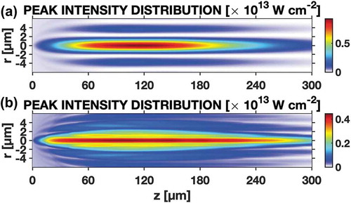
It is of interest to note a specific phenomenon of Bessel beams interaction with materials in strong excitation regimes. The high intensity on the axis generates carrier populations on the front of the laser pulse. The onset of carrier plasma along the core creates transient phase shifts for the conical wavelets and variations in the optical path, destabilizing the interference conditions for the annular ring . This can be seen in ) which compares the peak intensities of Bessel beams focused in vacuum ()) and Bessel beam focused inside a transparent material ()) at intensities high enough to generate electronic excitation and material structuring. The model takes into account nonlinear propagation based on nonlinear Schrödinger equation accounting for basic processes occurring in the presence of an intense laser field such as photoionization, free-carrier absorption, and collisional multiplication, as well as self-induced effects such as self-phase modulation, self-focusing, and plasma defocusing [Citation46]. Thus the interference condition determines bending and transient displacements in space of the position of the rings during the front of the laser pulse. The as-induced displacement matches the optical path variation generated by the electronic density achieved on the axis, smearing thus the average intensity on the rings. The consequence is a higher contrast between axis and rings and an actual filtering mechanisms producing structures only along the core in the material bulk for a wide range of input energies (see ).
Figure 7. Patterns of nonlinear light distributions during Bessel beam structuring modeled using nonlinear Schrödinger equation. (a) Bessel beam peak intensity in vacuum. (b) Bessel beam peak intensity in bulk fused silica in the presence of electronic excitation. A pulse of 3 ps and 7 µJ is used in a moderate focusing configuration (). A distortion of the rings in the presence of transient electronic excitation is to be noted.
4.3.4. Periodic nanoscale arrangements
A final example linking nanocavitation and light arrangement in periodic patterns refers to the onset of periodic arrangements of narrow sheets of void planes with transverse dimensions of few tens of nm and spaced at approximately , i.e. pattern periods in the range of 200–250 nm. These types of arrangements were first observed by Shimotsuma et al. [Citation20] and various hypotheses were in debate to account for their formation, including plasma waves [Citation20] or field-assisted deformation of nanoplasmas [Citation27]. Rudenko et al. [Citation104] explained the phenomenon by a light scattering mechanism on laser-induced microscopic scattering centers in near and far-fields, the coherent overlap of scattered wavelets and the onset of periodic standing waves. These scattering centers can originate from laser thermal and mechanical effects, including nanocracks and the nucleation of molecular decomposition centers [Citation105]. These nanocavities (sizes of 10 nm) can seed nanoplasmas in intense laser fields oriented according to the polarization, generate anisotropic scattering and create by interference periodic light plane patterns with sufficient carrier densities to generate opening of nanovoids [Citation106].
Albeit the different propagative character with respect to Gauss pulses, the nanogratings were equally observed under the incidence of Bessel beam [Citation107]. The interest here is that this phenomenon shows extreme light localization by coupling near-field waves and nanocavitation. An example is given in , showing experimental realization and numerical simulation of nanogratings. These are related to scattering and interference-driven modulation of light imprinting periodic patterns of electronic excitation as planes of dense carrier plasmas. Nanocavitation occurs at these sites creating the appearance of nanogratings, ordered nanocracks in the material. The anisotropic arrangements with directional scattering allows to define polarization functions.
Figure 8. (a) Nanogratings formed in fused silica under ultrafast multipulse Bessel irradiation. (b) Electromagnetic calculus of planes of electronic excitation suggesting the arrangement in nanoplanes under Bessel illumination. Data from Ref [Citation107].
![Figure 8. (a) Nanogratings formed in fused silica under ultrafast multipulse Bessel irradiation. (b) Electromagnetic calculus of planes of electronic excitation suggesting the arrangement in nanoplanes under Bessel illumination. Data from Ref [Citation107].](/cms/asset/c6e5fc93-f22f-4e3f-9e20-0436f39c6ee3/tapx_a_1659180_f0008_oc.jpg)
5. Conclusion
In conclusion we have shown that non-diffractive Bessel beams can generate material structuring of matter on scales smaller than the optical limit and with aspect ratios that enable a new range of laser-based machining applications. The feature size originates in material responses with characteristic scales given by hydrodynamic instabilities, favored by the specific one-dimensional geometry. The scale is ultimately defined by nanocavitation in solid or liquid phases and can achieve record values. While reviewing the excitation and relaxation paths, the process was discussed from a dynamic viewpoint. Controllability of the structural modification was shown, driven by the amount of excitation. The achievable scale opens interesting opportunities for material processing at the nanoscale, with in view structuring beyond the 100 nm benchmark in both direct focusing and self-organization regimes. The strong energy confinement alongside the high aspect ratio represent main features of the Bessel-Gauss beams. The structuring potential concerns applications requiring large scale interactions as well as high resolutions; from dicing to hybrid micro-nanophotonics. The potential of these beams to generate structures in two and three dimensions is being extrapolated to 2D materials [Citation108], hard matter [Citation109] and towards the use exotic profiles with extended flexibility [Citation110].
Acknowledgments
We would first like to thank the students and researchers who, by their contributions and results, enabled us to realize this review. We would like to thank K. Mishchik and F. Courvoisier for graciously providing us with images and M. Somayaji, G. Zhang, A. Mermillod-Blondin, P. K. Velpula, G. Martin, A. Soliehac and R. Antoine who, over the years, gathered data on Bessel laser processing and imaging.
Disclosure statement
No potential conflict of interest was reported by the authors.
Additional information
Funding
References
- Russbueldt P, Mans T, Rotarius G, et al. 400 W Yb: YAGInnoslab fs-amplifier. Opt Express. 2009;17:839–868.
- Sugioka K, Cheng Y. Ultrafast lasers–reliable tools for advanced materials processing. Light: Sci Appl. 2014;3:e149.
- Malinauskas M, Žukauskas A, Hasegawa S, et al. Ultrafast laser processing of materials: from science to industry. Light: Sci Appl. 2016;5:e16133.
- Poprawe R, Hinke C, Meiners W, et al. Digital photonic production along the lines of industry 4.0. SPIE Proceedings, Laser Applications in Microelectronic and Optoelectronic Manufacturing (LAMOM) XXIII; 2018;10519. p. 1051907.
- Abbe E, Lawson H. ed. A contribution to the theory of the microscope and the nature of microscopic vision. Proceedings of the Bristol Naturalists’ Society. Translated by Fripp HE. Vol. 1; London, UK: Williams & Northgate; 1876. pp. 200–261.
- Ashkenasi D, Rosenfeld A, Varel H. Wähmer, and Campbell EEB. Laser processing of sapphire with picosecond and sub-picosecond pulses. Appl Surf Sci. 1997;120:65–80.
- Joglekar AP, Liu H, Meyhöfer E, et al. Optics at critical intensity: Applications to nanomorphing. Proc Nat Acad Sci. 2004;101:5856–5861.
- Korte F, Serbin J, Koch J, et al. Towards nanostructuring with femtosecond laser pulses. Appl Phys A: Mater Sci Process. 2003;77:229–235.
- Klein-Wiele JH, Simon P. Sub-wavelength pattern generation by laser direct writing via repeated irradiation. Opt Express. 2013;21:626–630.
- Qin F, Huang K, Wu J, et al. A supercritical lens optical label-free microscopy: sub-diffraction resolution and ultra-long working distance. Adv Mater. 2017;29:1602721.
- Mishchik K, Petit Y, Brasselet E, et al. Patterning linear and nonlinear optical properties of photosensitive glasses by femtosecond structured light. Opt Lett. 2015;40:201–204.
- Korte F, Nolte S, Chichkov BN, et al. Far-field and near-field material processing with femtosecond laser pulses. Appl Phys A: Mater Sci Process. 1999;69:S7–S11.
- Chimmalgi A, Choi TY, Grigoropoulos CP, Komvopoulos K. Femtosecond laser aperturless near-field nanomachining of metals assisted by scanning probe microscopy. Appl Phys Lett. 2003;82:11461148.
- Falcón Casas I, Kautek W. Subwavelength nanostructuring of gold films by apertureless scanning probe lithography assisted by a femtosecond fiber laser oscillator. Nanomat. 2018;8:536.
- Piglmayer K, Denk R, Bäuerle D. Laser-induced surface patterning by means of microspheres. Appl Phys Lett. 2002;80:4693–4695.
- Ulmeanu M, Petkov P, Ursescu D, et al. Pattern formation on silicon by laser-initiated liquid-assisted colloidal lithography. Nanotechnology. 2015;26:455303.
- White YV, Li X, Sikorski Z, et al. Single-pulse ultrafast-laser machining of high aspect nano-holes at the surface of SiO2. Opt Express. 2008;16:14411–14420.
- Englert L, Rethfeld B, Haag L, et al. Control of ionization processes in high band gap materials via tailored femtosecond pulses. Opt Express. 2007;15:17855–17862.
- Rudenko A, Colombier JP, Höhm S, et al. Spontaneous periodic ordering on the surface and in the bulk of dielectrics irradiated by ultrafast laser: a shared electromagnetic origin. Sci Rep. 2017;7:12306.
- Shimotsuma Y, Kazansky PG, Qiu J, et al. Self-organized nanogratings in glass irradiated by ultrashort light pulses. Phys Rev Lett. 2003;91:247405.
- Abere MJ, Zhong M, Krüger J, et al. Ultrafast laser-induced morphological transformations. MRS Bull. 2016;41:969–974.
- Birnbaum M. Semiconductor surface damage produced by ruby lasers. J Appl Phys. 1965;36:3688–3689.
- Skoulas E, Manousaki A, Fotakis C, et al. Biomimetic surface structuring using cylindrical vector femtosecond laser beams. Sci Rep. 2017;7:45114.
- Dusser B, Sagan Z, Soder H, et al. Controlled nanostructrures formation by ultra fast laser pulses for color marking. Opt Express. 2010;18:2913–2924.
- Vorobyev AY, Guo C. Metal pumps liquid uphill. Appl Phys Lett. 2009;94:224102.
- Cheng G, Mishchik K, Mauclair C, et al. Ultrafast laser photoinscription of polarization sensitive devices in bulk silica glass. Opt Express. 2009;17:9515–9525.
- Taylor R, Hnatovsky C, Simova E. Applications of femtosecond laser induced self-organized planar nanocracks inside fused silica glass. Laser Photonics Rev. 2008;2:26–46.
- Zhang J, Gecevičius M, Beresna M, et al. Seemingly unlimited lifetime data storage in nanostructured glass. Phys Rev Lett. 2014;112:033901.
- Her TH, Finlay RJ, Wu C, et al. Microstructuring of silicon with femtosecond laser pulses. Appl Phys Lett. 1998;73:1673–1675.
- Halbwax M, Sarnet T, Delaporte P, et al. Micro and nano-structuration of silicon by femtosecond laser: Application to silicon photovoltaic cells fabrication. Thin Solid Films. 2008;516:6791–6795.
- Sipe JE, Young JF, Preston JS, et al. Laser-induced periodic surface structures. I Theory Phys Rev B. 1983;27:1141–1154.
- Grady DE. The spall strength of condensed matter J. Mech Phys Solids. 1988;36:353–384.
- Stoian R, Wollenhaupt M, Baumert T, et al. Temporal pulse tailoring in ultrafast laser manufacturing technologies. In: Sugioka K, Meunier M, Pique A, editors. Laser precision microfabrication, springer series in optical sciences. Vol. 135. Heidelberg: Springer Verlag; 2010. p. 121–144.
- Marcinkevičius A, Juodkazis S, Matsuo S, et al. Application of Bessel beams for microfabrication of dielectrics by femtosecond Laser. Jpn J Appl Phys. 2001;40:L1197–L1199.
- Zambon V, McCarthy N, Piché M Laser micromachining of transparent glass using ultrafast Bessel beams. Proc. SPIE 7386; Aug 4; Photonics North; 2009. p. 738632.
- Mitra S, Chanal M, Clady R, et al. Millijoule femtosecond micro-Bessel beams for ultra-high aspect ratio machining. Appl Opt. 2015;54:7358–7365.
- Yang L, Qian D, Xin C, et al. Two-photon polymerization of microstructures by a non-diffraction multifoci pattern generated from a superposed Bessel beam. Opt Lett. 2017;42:743–746.
- Matushiro Y, Watanabe W. Femtosecond laser processing of polymethyl methacrylate with an axicon. J Las Micro Nanoeng. 2016;11:59–65.
- Tsampoula X, Garcés-Chávez V, Comrie M, et al. Femtosecond cellular transfection using a nondiffracting light beam. Appl Phys Lett. 2007;91:053902.
- Dudutis J, Gečys P, Račiukaitis G. Non-ideal axicon-generated Bessel beam application for intra-volume glass modification. Opt Express. 2016;25:28433–28443.
- Durnin J, Miceli JJ, Eberly JH. Diffraction-free beams. Phys Rev Lett. 1987;58:1499–1501.
- Sheppard C, Wilson T. Gaussian-beam theory of lenses with annular aperture. IEE J Microw Opt Acoust. 1978;2:105–112.
- McLeod JH. The axicon: a new type of optical element. J Opt Soc Am. 1954;44:592–597.
- Herman RM, Wiggins TA. Production and uses of diffractionless beams. J Opt Soc Am A. 1991;8:932–942.
- Gori F, Guattari G, Padovani C. Bessel-Gauss beams. Opt Commun. 1987;64:491–495.
- Velpula PK, Bhuyan MK, Courvoisier F, et al. Spatio-temporal dynamics in nondiffractive Bessel ultrafast laser nanoscale volume structuring. Laser Photonics Rev. 2016;2:230–244.
- McGloin D, Dholakia K. Bessel beams: diffraction in a new light. Contemp Phys. 2005;46:15–28.
- Duocastella D, Arnold C. Bessel and annular beams for materials processing. Laser Photonics Rev. 2012;6:607–621.
- Čižmár T, Dholakia K. Tunable Bessel light modes: engineering the axial propagation. Opt Express. 2009;17:15558–15570.
- He F, Yu J, Tan Y, et al. Tailoring femtosecond 1.5 µm Bessel beams for manufacturing high-aspect-ratio through-silicon vias. Sci Rep. 2017;7:40785.
- Bhuyan MK, Velpula PK, Somayaji M, et al. 3D Nano-fabrication using controlled Bessel–glass interaction in ultrafast modes. J Las Micro Nanoeng. 2017;12:274–280.
- Meyer R, Froehly L, Giust R, et al. Extremely high-aspect-ratio ultrafast Bessel beam generation and stealth dicing of multi-millimeter thick glass. Appl Phys Lett. 2019;114:201105.
- Mcleod E, Arnold CB. Subwavelength direct-write nanopatterning using optically trapped microspheres. Nat Nanotechnol. 2008;3:413–417.
- Bhuyan MK, Courvoisier F, Lacourt PA, et al. High aspect ratio nanochannel machining using single shot femtosecond Bessel beams. Appl Phys Lett. 2010;97:081102.
- Amako J, Sawaki D, Fujii E. Microstructuring transparent materials by use of nondiffracting ultrashort pulse beams generated by diffractive optics. J Opt Soc Am B. 2003;20:2562.
- Mikutis M, Kudrius T, Šlekys G, et al. High 90% efficiency Bragg gratings formed in fused silica by femtosecond Gauss-Bessel laser beams. Opt Mat Express. 2013;3:1862–1871.
- Mishchik K, Beuton R, Dematteo–Caulier O, et al. Improved laser glass cutting by spatio-temporal control of energy deposition using bursts of femtosecond pulses. Opt Express. 2017;25:33271–33282.
- Rapp L, Meyer R, Furfaro L, et al. High speed cleaving of crystals with ultrafast Bessel beams. Opt Express. 2017;25:9312–9317.
- Dudutis J, Stonys R, Račiukaitis G, et al. Glass dicing with elliptical Bessel beam. Opt Laser Technol. 2019;111:331–337.
- Zhang G, Stoian R, Zhao W, et al. Femtosecond laser Bessel beam welding of transparent to non-transparent materials with large focal-position tolerant zone. Opt Express. 2018;26:917–926.
- Jenne M, Flamm D, Ouaj T, et al. Glass cutting optimization with pump-probe microscopy and Bessel beam profiles. Proc SPIE. 2018;10522:1052216.
- Jenne M, Flamm D, Ouaj T, et al. High-quality tailored-edge cleaving using aberration-corrected Bessel-like beams. Opt Lett. 2018;43:2164–2167.
- Stoian R, Bhuyan MK, Cheng G, et al. Ultrafast Bessel beams; advanced tools for laser material processing. Adv Opt Technol. 2018;7:165–174.
- Meyer R, Jacquot M, Giust R, et al. Single-shot ultrafast laser processing of high-aspect-ratio nanochannels using elliptical Bessel beams. Opt Lett. 2017;43:4307–4310.
- Orlov S, Vosylius V, Gotovski P, et al. Vector beams with parabolic and elliptic cross-sections for laser material processing applications. J Las Micro Nanoeng. 2018;13:280–286.
- Alexeev I, Leitz HK, Otto A, et al. Application of Bessel beams for ultrafast laser volume structuring of non transparent media. Phys Procedia. 2010;5:533–540.
- Nguyen HD, Sedao X, Faure N, et al. Advanced ultrafast laser Bessel beam for machining metallic materials. Paper presented at: LAMP 2019 International Congress on Laser Advanced Materials Processing; 2019 May 21–24; Hiroshima, Japan.
- Liu X, Li Q, Sikora A, et al. Truncated Gaussian-Bessel beams for short-pulse processing of small-aspect-ratio micro-channels in dielectrics. Opt Express. 2019;27:6996–7008.
- Zhang Y, Zhang GD, Chen C, et al. Transmission volume phase holographic gratings in photo-thermo-refractive glass written with femtosecond laser Bessel beams. Opt Mat Express. 2016;6:3491–3499.
- Zhang G, Cheng G, D’Amico C, et al. Efficient point-by-point Bragg gratings fabricated in embedded laser-written silica waveguides using ultrafast Bessel beams. Opt Lett. 2018;43:2161–2164.
- Martin G, Bhuyan MK, Troles J, et al. and Le Coarer E. Near infrared spectro-interferometer using femtosecond laser written GLS embedded waveguides and nano-scatterers. Opt Express. 2017;25:8386–8397.
- Le Coarer E, Blaize S, Benech P, et al. Wavelength-scale stationary-wave integrated Fourier-transform spectrometry. Nat Photonics. 2007;1:473–478.
- Gadonas R, Jarutis V, Paškauskas R, et al. Self-action of Bessel beam in nonlinear medium. Opt Commun. 2001;196:309–316.
- Faccio D, Rubino E, Lotti A, et al. Nonlinear light-matter interaction with femtosecond high-angle Bessel beams. Phys Rev A. 2012;85:033829.
- Polesana P, Franco M, Couairon A, et al. Filamentation in Kerr media from pulsed Bessel beams. Phys Rev A. 2008;77:043814.
- Itoh K, Watanabe W, Nolte S, et al. Ultrafast processes for bulk modification of transparent materials. MRS Bull. 2006;31:620–625.
- Balling P, Schou J. Femtosecond-laser ablation dynamics of dielectrics: basics and applications for thin films. Rep Prog Phys. 2013;76:036502.
- Gattass RR, Mazur E. Femtosecond laser micromachining in transparent materials. Nat Photonics. 2008;2:219–225.
- Davis KM, Miura K, Sugimoto N, et al. Writing waveguides in glass with a femtosecond laser. Opt Lett. 1996;21:1729–1731.
- Glezer EN, Mazur E. Ultrafast-laser driven micro-explosions in transparent materials. Appl Phys Lett. 1997;71:882–884.
- Martin P, Guizard S, Daguzan P, et al. Subpicosecond study of carrier trapping dynamics in wide-band-gap crystals. Phys Rev B. 1997;55:5799–5810.
- Audebert P, Daguzan P, Dos Santos A, et al. Space-time observations of an electron gas in SiO2. Phys Rev Lett. 1994;73:1990–1993.
- Watanabe M, Juodkazis S, Sun H, et al. Luminescence and defect formation by visible and near-infrared irradiation of vitreous silica. Phys Rev B. 1999;60:9959–9964.
- Chan J, Huser T, Risbud S, et al. Modification of the fused silica glass network associated with waveguide fabrication using femtosecond laser pulses. Appl Phys A: Mater Sci Process. 2003;76:367–372.
- Mishchik K, D’Amico C, Velpula PK, et al. Ultrafast laser induced electronic and structural modifications in bulk fused silica. J Appl Phys. 114:133502.
- Lancry M, Poumellec B, Chahid-Erraji A, et al. Dependence of the femtosecond laser refractive index change thresholds on the chemical composition of doped-silica glasses. Opt Mat Express. 2011;1:711–723.
- Eaton SM, Zhang H, Herman PR, et al. Heat accumulation effects in femtosecond laser written waveguides with variable repetition rate. Opt Express. 2005;13:4708–4716.
- Liu Y, Shimizu M, Zhu B, et al. Micromodification of element distribution in glass using femtosecond laser irradiation. Opt Lett. 2009;34:136–138.
- Yu Y, Jian L, Cao Q, et al. Pump-probe imaging of the fs-ps-ns dynamics during femtosecond laser Bessel beam drilling in PMMA. Opt Express. 2015;23:32728–32735.
- Ahn S, Choi J, Noh J, et al. High aspect ratio nanoholes in glass generated by femtosecond laser pulses with picosecond intervals. Opt Laser Eng. 2018;101:85–88.
- Bhuyan MK, Velpula PK, Colombier JP, et al. Single-shot high aspect ratio bulk nanostructuring of fused silica using chirpcontrolled ultrafast laser Bessel beams. Appl Phys Lett. 2014;104:021107.
- Bhuyan MK, Somayaji M, Mermillod-Blondin A, et al. Ultrafast laser nanostructuring in bulk silica, a “slow” microexplosion. Optica. 2017;4:951–958.
- Vailionis A, Gamaly EG, Mizeikis V, et al. Evidence of super-dense aluminium synthesized by ultrafast microexplosion. Nat Comm. 2011;2:445.
- Rapp L, Haberl B, Pickard CJ, et al. Evidence of new tetragonal polymorphs of silicon formed through ultrafast laser-induced microexplosion. Nat Comm. 2015;6:7555.
- Juodkazis S, Nishimura K, Tanaka S, et al. Laser-induced microexplosion in the bulk of a sapphire crystal: Evidence of Mb pressures. Phys Rev Lett. 2006;96:166101.
- Beuton R, Chimier B, Brei J, et al. Thermo-elasto-plastic simulations of femtosecond laser-induced multiple-cavity in fused silica. Appl Phys A: Mater Sci Process. 2018;124:324.
- Wang J, Rajendran AM, Dongare AM. Atomic scale modeling of shock response of fused silica and a-quartz. J Mater Sci. 2015;50:8128–8141.
- Juodkazis S, Misawa H, Gamaly EG, et al. Is the nano-explosion really microscopic? J. Non-Cryst Solids. 2009;355:1160–1162.
- Kraus RG, Stewart ST, Swift DC, et al. Shock vaporization of silica and the thermodynamics of planetary impact events. J Geophys Res. 2012;117:E09009.
- Melosh H. A hydrocode equation of state for SiO2. Meteorit Planet Sci. 2007;42:2079–2098.
- Medvedev AB. Equation of state of silicon dioxide with allowance for evaporation, dissociation, and ionization. Combust Explos Shock Waves. 2016;52:463–475.
- Eggers J. Nonlinear dynamics and breakup of free-surface flows. Rev Mod Phys. 1997;69:865–930.
- Rapp L, Meyer R, Giust R, et al. High aspect ratio micro-explosions in the bulk of sapphire generated by femtosecond Bessel beams. Sci Rep. 2016;6:34286.
- Rudenko A, Colombier JP, Itina TE. From random inhomogeneities to periodic nanostructures induced in bulk silica by ultrashort laser. Phys Rev B. 2016;93:075427.
- Lancry M, Poumellec B, Canning J, et al. Ultrafast nanoporous silica formation driven by femtosecond laser irradiation. Laser Photonics Rev. 2013;7:953–962.
- Rudenko A, Colombier JP, Itina TE. Nanopore-mediated ultrashort laser-induced formation and erasure of volume nanogratings in glass. Phys Chem Chem Phys. 2018;20:5887–5899.
- Cheng G, Rudenko A, DAmico C, et al. Embedded nanogratings in bulk fused silica under non-diffractive Bessel ultrafast laser irradiation. Appl Phys Lett. 2017;110:261901.
- Gil-Villalba A, Xie C, Salut R, et al. Deviation from threshold model in ultrafast laser ablation of graphene at sub-micron scale. Appl Phys Lett. 2015;107:061103.
- Kumar S, Eaton SM, Bollani M, et al. Laser surface structuring of diamond by means of pulsed Bessel beams. Sci Rep. 2018;8:14021.
- Xie15 Xie C, Jukna V, Milián C, et al. Tubular filamentation for laser material processing. Sci Rep. 2015;5:8914.