
ABSTRACT
Neuroscience deals with one of the most complicate system we can study: the brain. The huge amount of connections among the cells and the different phenomena occurring at different scale give rise to a continuous flow of data that have to be collected, analyzed and interpreted. Neuroscientists try to interrogate this complexity to find basic principles underlying brain electrochemical signalling and human/animal behaviour to disclose the mechanisms that trigger neurodegenerative diseases and to understand how restoring damaged brain circuits. The main tool to perform these tasks is a neural interface, a system able to interact with brain tissue at different levels to provide a uni/bidirectional communication path.
Recently, breakthroughs coming from various disciplines have been combined to enforce features and potentialities of neural interfaces. Among the different findings, flexible electronics is playing a pivotal role in revolutionizing neural interfaces.
In this work, we review the most recent advances in the fabrication of neural interfaces based on flexible electronics. We define challenges and issues to be solved for the application of such platforms and we discuss the different parts of the system regarding improvements in materials selection and breakthrough in applications both for in vitro and in vivo tests.
Graphical Abstract
1. Introduction
Neuroscience is a multidisciplinary branch of the knowledge that has the aim of explaining the behaviour of the central nervous system [Citation1]. Neuroscience has the ultimate objective of connecting the neurons action potential with the living beings’ behaviours. The complexity of the challenges is clear: a huge amount of morphological, functional and physical information coming from the neural tissue have to be collected and analyzed. Moreover, the number of involved cells during a single event and the bundle of different phenomena happening from a specific neuron to a large population of cells make the findings difficult to achieve.
At the single neuron scale, in fact, studies are focused on investigating intracellular current, ion channel activation and synaptic current, down to dendritic spines behaviour, while, at mesoscale, small organized region of the brain like cortical columns reveal specific tasks. The columns interactions, at large scale of the brain areas, turn into movement control, process information, inhibit actions but also generate emotions and ideas. Practically, everything we call the human behaviour.
These three levels of information that go from the single neurons to the functional areas of the brain passing through the small-organized areas of neural system need to be grabbed and controlled. This means managing investigation analysis methods that face the different issues and level of details that the single analysis requires. Large areas of brain can be monitored by mapping an external electrical activity with electroencephalography (EEG) or using imaging technique, such as functional magnetic resonance (fMRI) and positron emission tomography (PET) [Citation2–Citation4]. On the other hand, the conventional method, used by electrophysiologists to obtain direct information from specific parts of the brain, is a passive recording of neurons spontaneous activity or triggered by some stimulation (that can be electrical, visual, pharmacological, etc.). This methodology relies on the measurement of the local field potentials (LPFs) caused by the superimposition of multiple potentials generated in the extracellular medium by neuronal activity [Citation5]. Finally, the techniques used to investigate the single neurons behaviour span from patch-clamp to two-photon imaging. All these techniques include a very different level of invasiveness and tools for acquiring signals and comprehend their nature.
Nowadays, electronics provides unique equipment to monitor the different brain functions and offers the integration of new investigating techniques. New integrated devices that we call neural interfaces have substituted the classical cumbersome laboratory equipment that is generally split in separated tools. We define a neural interface an all-in-one electronic platform able to record, amplify, digitalize and classify neural signals in real time. A neural interface can be a fully implantable device or a partially implantable one depending by the needs but generally is an invasive tool. A neural interface can open new opportunities in electrophysiology, especially if integrating also stimulation sub-system, it allows usage of closed-loop algorithms that were impeded from the high latencies of the old diverse devices.
This platform enables neuroscientists also to collect and define differences between healthy people and patients with neurological disorders both for early diagnosis of diseases and for activity restoring. Particularly for patients with tetraplegia or partial paralysis, these neural interfaces can represent a unique opportunity to partially restore some physiological functions or to create neural bypass enabling them to control hand gestures or limb movements [Citation6–Citation9].
Numerous review papers reported new findings in the part that is usually in contact with the brain, such as the electrode grid [Citation10–Citation13] and described physiological mechanisms underlying the implantation of these devices in the brain [Citation14], but very few present all the fabrication methodologies that involve new materials and electronic design to allow the manufacturing of the whole system.
In this review, we will overview how flexible electronics can revolutionize neural interfaces and how novel fabrication strategies of flexible circuits and components can help scientists to manufacture innovative neural implants with additional functionalities. We will introduce the different kinds of electrode grids and the types of electronics integrated in the part of the device devoted to signal amplification, filtering and digitalization with the idea of showing the entire neural interface in all its faceting. This tool can shed a new light on the brain activity offering extra functionalities, substituting rigid recording components with ultra-flexible and conformable wireless devices able to interact with the cerebral cortex in a bidirectional way [Citation15,Citation16]. We think improvements brought from the flexible electronics may improve neuroscientist’s knowledge of the brain, indeed, despite numerous findings about many computational principles of the cerebral cortex underlying network dynamic pattern, many aspects remain unclear. For example, the role of glial cells, which represents the majority of the brain cells, is still controversial losing the old neuroscientists’ perspective of merely supporting elements to active structures for the control of synaptic activity with an extracellular autonomous activity [Citation17].
With the aim of improving functionalities in neural interfaces and managing the amount of information that can be detected during measurements, flexible electronics is assuming increasingly importance in neuroscience. For flexible electronics we intend a technology that enables the fabrication of bendable or rollable platform on which electronic circuits and sensors are integrated. If the circuitry can be even stretched without losing its properties we refer to stretchable electronics. This type of electronics dates back to the 1960s when for the first time solar cell arrays were assembled on a plastic substrate [Citation18]. In the same decade, the first flexible transistor was proposed by the group of Brody opening the way for the development of active matrix liquid crystal displays (AMLCDs) in the 1990s [Citation19]. In the 2000s, printed organic electronics appears promising to drastically reduce time and costs of fabrication. In few years, chemists synthetized a huge variety of new organic materials creating interesting opportunities for very different applications. Moreover, depending by the application, other properties can be added like transparency (for instance for smart displays used in automotive) [Citation20], material biocompatibility (in case of biomedical devices), breathability (for skin smart patch) [Citation21], biodegradability (for low-cost disposable devices for instance in precise agriculture) [Citation22] and many other utilized in wearable application, e.g. sportswear, smart toys, etc. [Citation23,Citation24].
Borrowing the same terminology used in other electronic fields such as consumer electronics, we can divide active materials embedded in flexible substrates in three big categories: (i) Silicon-based materials, (ii) Metal Oxide materials and (iii) Organic materials. Each of these technologies exhibits different properties that make them suitable for specific applications. In biology, none of the above-mentioned technologies are precluded, but inorganic-based electronics seems to be more robust. In fact, even if biological events are intrinsically slow (typically not above kHz) biocompatibility, electrical and mechanical stability, electrical mobility and process integrability are preferred especially in case of long-term implants. These considerations become truer when we consider the increasing demand of high-density recording system with hundreds of channels to be managed in real-time.
The implementation of a specific material defines also the technologies adopted to fabricate the desired application: in case of silicon and metal oxide devices, conventional microelectronic equipment is used while for organic materials roll-to-roll systems are preferred. The first scenario usually involves the usage of temporary supports for handling the prototypes keeping process temperature below values that polymer can stand (up to 300°C) or a subsequent integration of the electronics in forms of a thin sheet of few microns into a flexible substrate by wafer thinning or lamination. In the second case, engineers deposit materials directly on the rolling foils usually without vacuum system in a set of glow box or in air, manufacturing devices in few hours but with a lower material quality. Indeed, if we adopt electrical mobility as key parameter to define the cut-off frequency of the electronics (that means the maximum speed at which system can operate), we can roughly assume the fastest manufacturing process coincides with the lower mobility of the electronic components. In , we report the average values of electrical mobility for thin film transistors with comparable dimensions.
Table 1. All the values are referred to transistors tested at room temperature for a fixed W/L geometry.
The choice of the flexible substrate as well as the material used for encapsulation is pivotal in the design of the electronic system especially in case of implants. First the material must meet a number of fundamental conditions to be selected as a possible candidate for a neural interface: this material should be bio-inert or at least biocompatible, depending by the application (chronic or acute). It should have low surface roughness (below 10 nm), low thermal expansion coefficient (few ppm/°C), low elastic modulus (from few GPa to few kPa) and be possibly characterized by a high glass transition temperature (>250°C). Surface roughness can be mitigated using deposition techniques that involve a starting liquid phase of the film such as spin-coating are preferred. These methods provide smooth surfaces with an average roughness below 10 nm and can act as valuable procedure to fabricate device substrate, as well as passivation layer. Especially in thin film technology, low surface roughness is also a key requirement to avoid the formation of cracks and hillock in the upper layers that can produce delamination and device failure. Another important aspect for the choice of the substrate is the coefficient of thermal expansion (CTE). During neural interface fabrication, especially in hybrid systems, where inorganic materials are integrated or grown on polymeric films, temperature variations can induce a strain into the different layers according to their CTE mismatch. In some cases, this phenomenon brings a permanent bending of the device. If this strain is too high, the upper film can lose adhesion thus forming cracks. Moreover, thermo-mechanical effects can be detrimental due to the tendency of polymeric materials to shrink at specific temperature. This issue can be mitigated by applying prolonged annealing at the maximum process temperature to stabilize the dimensions of the substrate. Finally, in case of inorganic materials, the direct integration of electronic components in the substrate involves the deposition of metals, semiconducting and insulating films at temperatures from 250°C to 350°C and sometimes fast heat treatments (e.g. laser annealing) are required to induce a suitable recrystallization in the material thus enhancing its electrical quality. Moreover, even after the devices fabrication, some processes such as sterilization may occur without affecting operability of the electronic systems. Different polymers have been proposed as substrate or passivation layer for flexible electronics including Polyimide, Polydimethylsiloxane (PDMS), Parylene, Durimides, Kapton, etc. [Citation25–Citation30].
Another key parameter to be considered is the degree of bendability and stretchability of the entire system: brain is a pulsatile organ and a neural interface on the cerebral cortex tends to follow the brain movements thus shifting on the surface and losing specific recording areas or worst triggering inflammatory response of the tissue. For this reason, a certain level of stretchability is preferred when an active neural interface is designed. Three strategies may be used in this case, adopting intrinsic stretchable materials (such as PDMS) [Citation31], tailoring a network of rigid islands or membranes [Citation32] or exploiting buckling structures that can deform without suffering of crack and delamination [Citation33]. The capability of monitoring and interacting with a localized part of the brain for long periods represents a key task to recognize specific pattern, to control neurological functions in patients affected by neuro disorders and to infuse precise spatial-temporal stimulation at fixed times.
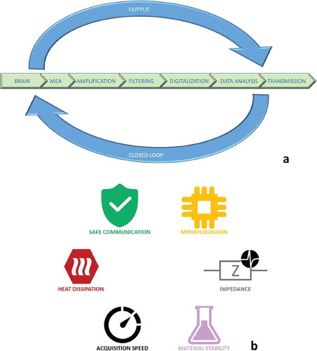
To summarize, as described in ), a neural interface includes several parts that confers the platform the capability to measure, filter, digitalize, store and communicate the signals recorded on the brain or provide stimulation after the individuation of specific pattern (data analysis). Typically, we have a set of electrodes directly on the brain that can be placed inside the tissue or on the cortex (subdural or epidural grid). A bundle of conductive tracks brings the brain signals to a pre-amplification stage since the amplitude of the recordings is in the range of microvolts in case of epicortical electrodes. Then filters and digitalization modules transform analogical signals and classification occurs. In these years, the trend for neural interface tends to localize the electronics and the algorithms for signal classification close to the grid in order to maximize signal-to-noise ratio (SNR), reduce latency and avoid communication issues, thus permitting the usage of fully autonomous systems. In the following sections, we will systematically review the materials and technologies utilized for the manufacturing of the different parts of a neural interface starting from the grid to the type of electronics that can be embedded in a flexible platform to fabricate a portable, implantable and autonomous device.
Figure 1. (a) A schematic representation of a neural interface divided in its main components; (b) some critical aspects to be considered for the designing of a performing neural interface.
2. Brain challenges
Human brain is one of the most complicate structures that can be observed on Earth. A small portion of human cerebral cortex of about 1 mm3 can contain up to 5 × 10⁴ neurons and four times as many as glial cells. Additionally, each neuron embraces about 6 × 10³ of computational elements in a network of 300 million connections. In the sole cerebral cortex, it can be found bundles of neurons with very different form (e.g. pyramidal, chandelier, basket, double bouquet, etc.) and tasks. The majority are excitatory pyramidal cells while a 20% of the neurons act as inhibitory cells. Neurons are located in one of the six layers of the cortex, referring to their cell body, while their connections can span thought the layers and reach the cortex surface. The communication occurs vertically between layers and horizontally through the layers, defining functional specialization areas across the surface of the cortex. According to a principle of economic wiring, the cortex controls input and output by preferring communication along vertical column-like arrays that for their intrinsic structure are called cortical columns or functional columns [Citation34,Citation35]. Many scientists have hypothesized that columns can be the main source of processing for the cortex in humans and other primates. Other scholars suggest that a fine-grain functional modularity of micro-columns exists, referring to a narrow vertical region in which all neurons have virtually identical receptive field locations, sizes and shapes [Citation36]. These physiological considerations automatically define the correct size and spacing of surface electrodes to guarantee the detection of information without redundancy and without potential losses. Indeed, neuroscientists can obtain a lot of information analysing signals coming from the different layers of cerebral columns that in humans are in the range of hundreds of microns. For other mammalians, these diameters can be even smaller and this is the reason why high-resolution neural recordings need hundreds of electrodes with a spacing ranging from 500 to 50 µm depending by the type of animal. This sub-millimetre spatial resolution is also particularly useful for the observations of pathological brain signals in epileptic brain or in other neurological disorders [Citation37]. In fact, cerebral cortex can collect signals coming from the axons and dendrites placed in the six layers. This is the environment in which a neural interface has to be deployed in order to successfully collect the electrochemical signals.
It is important to note that when a neural interface is inserted in the brain, a foreign body reaction takes place producing potential issues for both the brain tissue and the implant: in fact, due to the stress related to implantation surgery and to the following mechanical micro-movements in the brain the tissue reacts creating a thin encapsulating layer with microglia cells in just one day. After this first reaction, astrocytic glial cells form a second thicker barrier in one or two weeks, limiting ionic diffusion and separating the neural interface by the selected recording site. Finally, the glial scar formation is completed in a period of about six weeks producing a stable compact layer of cells. This is the main factor that limits the correct operation of a long-term implant that should be desirably active for the entire lifetime of the patient. To minimize this mechanism, four strategies can be adopted: the usage of soft materials, the implementation of surface coating to prevent biofouling, the integration of drug delivery system to control the inflammatory mechanism and the engineering of autologous cell layer to suppress the tissue response [Citation14]. On the implant side, other issues arise in term of durability and reliability. In fact, in long-term implants, due to the activation of immune cells, which release digestive enzymes and reactive oxygen species, corrosion and delamination of the conductive materials can take place, thus leading to the device failure [Citation38].
3. Neural interface
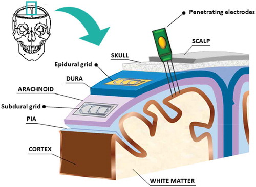
We refer to a neural interface or to brain computer interface (BCI) as a complex system able to collect signals coming from the brain or its surface and transduces this information into valuable data to create a bidirectional interaction. This device can simply monitor the brain activity to identify healthy and pathological pattern or can induce specific body response by stimulating or inhibiting some neural circuits. As described in , the neural interface can be sketched as a system composed of several parts that can be all integrated into a small prototype (as in case of brain implants) or can be distributed in different components. The first part of such a system, which directly touches the living tissue or cells culture (e.g. for in vitro applications), is the grid. A grid is generally a flexible surface on which a series of electrodes are deployed together with some additional electronic modules depending by the case. We often call the grid in many different ways: the most common are microelectrodes arrays (MEAs) in which we include both planar electrodes and implantable probes. A grid exhibits several features and it can be divided into many categories: it can be passive or active, composed only of conductive tracks or pre-amplified recording sites. A grid can be fully planar or adopt protrusions, needles or nanostructures to achieve a stronger adhesion with the tissue or the cells, thus improving the quality of the signal. With the same terminology, we can include electrodes designed for only neural recording or for both recording and stimulation, probes designed for exclusively acute applications or long-term implants and devices fabricated for in vivo applications or in vitro experiments.
Figure 2. A sketch showing the parts of head where grids can be placed to collect signals from the cortex: subdural devices, epidural devices and penetrating electrodes. Non-invasive electrodes have not been taken into account in this scheme.
As highlighted in ), some critical features have to be considered in the designing of a neural interface: all the materials of the system should be stable in time, especially if we think to implants, to avoid inflammation of the brain tissue or even release of toxic materials. Temperature must be kept below 40°C during operation in any configuration of the system, it means a maximum heat flux of 40 mW/cm2 [Citation39] or a specific absorption rate (SAR) limit (averaged over any 10 g of tissue) of 0.4 W/kg on whole body or 10 W/kg localized for radiation from 100 kHz to 3 GHz [Citation40]. Therefore, low power consumption modules are preferred. Moreover, heat dissipation of each part of the neural interface should be carefully considered and measured mitigating self-heating effects with the insertion of specific materials (this aspect is pivotal in polymeric platforms). For high-density electrodes arrays, strategies for the minimization of impedance (e.g. nanocoating) have to be adopted to guarantee the detection of small signals especially in epidural devices. Another important aspect is the total bandwidth available to be shared through the different recording sites. Finally, a reliable communication protocol should take into account a trade-off between the amount of data to transmit to external devices and the level of redundancy with which data are transmitted.
For long-term implants these argues are even more stringent, especially if we talk about materials stability and tissue response. Indeed, stiffness mismatch between the brain tissue and the probe substrate represents the main cause of implant failure. Brain is relatively soft with a Young’s Modulus of few kPa, while even flexible MEAs based on polyimide, SU-8 or Parylene are in the range of few GPa [Citation10]. Conversely, soft polymers like PDMS show similar brain stiffness but result difficult to handle and cannot be easily manufactured in ultra-thin layers. Another critical aspect relies on the surgical insertion on the neural interface: the organism, in fact, always perceives the platform as a foreign body and it triggers an acute inflammation that turns into a chronic neuroinflammatory response thus altering the normal functions on the region in which the neural interface is placed. This condition becomes more critical if we consider normal movements of the brain due to the cardiac rhythm and breath. Two main strategies can be adopted to minimize this issue: the use of ultra-flexible substrates or the implementation of stretchable polymers [Citation41]. In both cases, handling problems remain a technological barrier, but a sacrificial bio-compatible material (e.g. silk) [Citation42] can be exploited to temporary permit the surgical insertion.
3.1. Passive grids
As above-mentioned, the grid is the part of the neural interface in contact with the brain where the signals are generated. Generally, these devices are commonly called MEAs and they are the evolution of the original idea to fabricate a tool enabling the interfacing with electrically excitable cells like neurons. The Italian physicist Luigi Galvani first discovered bioelectricity in 1789 opening a new way of understanding the electrical processes in living cells [Citation43]. Only a century later, another Italian scientist Camillo Golgi [Citation44] discovered that neural tissue is composed of the neurons (1873) [Citation44]. In the same period, the Spanish scientist Santiago Ramon y Cajal identified that neurons are distinct cells connected among them [Citation45], and he definitively proposed of accepting the name neuron, suggested by the German Scientist Heinrich von Wilhelm [Citation46], to identify the cells of the neural system. Then, it was a long time before we had a technology that allowed the direct measurement of action potentials. Indeed, in the late 1930s, A. L. Hodgkin and F. Huxley reported this result inserting an electrode into the giant axons of a squid [Citation47]. Microelectrodes for intracellular recording of spinal cord and their understanding date back to 1950s [Citation48] and 1960s [Citation49], while Thomas proposed the first miniaturized microelectrode for extracellular recording of cultured cells in 1972 [Citation50]. Later, Pine and Gross significantly contributed to increase the spreading of these devices as a pivotal in vitro tool [Citation51,Citation52]. The first flexible MEAs appeared in the early 1980s [Citation53] and they became thinner in the 1990s [Citation54], assuming the features they usually have nowadays.
Flexible MEAs are essentially composed of interposing conductive electrodes in two polymer foils one used as substrate and the other as passivation layer with opened vias to connect sensing areas directly with the brain tissue (see )), albeit capacitive electrodes have been also proposed [Citation55]. We can divide flexible electrodes in three main categories according to the type of conductive material integrated in the grid: (i) metals, (ii) metal oxides and (iii) carbon like blends. Each type of materials has peculiar advantages respect to other, demonstrating in some case superior performance in recording or under prolonged stimulation. These differences intrinsically depend by the nature of the signals that have to be detected: in neurons, signals are generated by the ions’ movements (e.g. Na+ and K+) through cell membrane, thus locally modifying ions concentrations in the extracellular fluid (ECF). This ion current must be transformed into electron current to detect neuron signals. Each material responds to this task peculiarly depending also by temperature, pH and electrode surface morphology. This property, enabling a conductive film to efficiently perform charge transfer, is defined by three main factors: impedance, charge storage capacity (CSC) and charge injection limit (CIL) [Citation13]. Generally, planar metallic electrodes show high conductivity but only good charge transfer, while metal oxides like iridium oxide exhibits large CIL [Citation56] and conducting polymers can reach huge CSC [Citation57]. Moreover, conductive polymers can be chemically modified and mixed with different nanostructures. Among the diverse conductive polymers, it is worth mentioning polythiophene [Citation58], PEDOT [Citation59,Citation60], Polypyrrole (PPy) [Citation61]. Another option is the formation of conductive metal/polymer nanocomposite (e.g. Pt/SU8 or Au/PDMS) by using nanoparticles implantation technique [Citation62,Citation63]. Conversely, nanoporosity or direct growth of nanostructures on metallic electrodes can greatly enhance their performance in terms of impedance reduction [Citation64,Citation65]. Recently, on carbon-based material side, graphene is emerging as attractive solution for neural applications due to its high charge carrier mobility, transparency and mechanical strength [Citation66].
Figure 3. (a) A sketch showing the fundamental elements of a passive grid: a conductive film embedded into two layers of flexible polymeric materials; (b) the five properties that enhance grid functionalities to overcome challenges for a high-density recording/stimulating active grid.
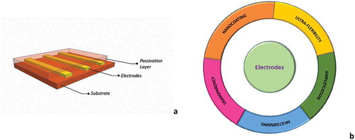
) represents five main features that can drastically enhance electrodes properties upgrading these devices to a new level of complexity, thus permitting a combination of functionalities and testing techniques. These five keywords are nanocoating, ultra-flexibility, transparency, multi-sensing and local amplification. They are related to the possibility to minimize electrodes impedance, reduce inflammatory response of the tissue and adding novel insight about the chemical and the physical microenvironment in which neurons communication take place.
As first issue in MEAs design and manufacturing, we report impedance control when electrodes are scaling down to few tens of micrometre: size reduction is mandatory to communicate with individual or few neurons without damaging the tissue, while maintaining high SNR. Strategies to tackle this issue focus on increasing the effective surface area by shifting from metal or metal-oxide thin films toward nanostructured electrodes, such as carbon nanotubes (CNTs) [Citation67], polymer-CNT meshes [Citation68], Au nanostructures [Citation69,Citation70] doped diamond [Citation71] and graphene [Citation72], mushroom-shaped gold microstructures [Citation73] and semiconductor nanowires (NWs) [Citation74–Citation77].
Nano-coating is also playing a relevant role in reducing the immune reaction in long-term implants, as demonstrated by some smart encapsulation mechanisms (e.g. hydrogel-based layer) [Citation78]. In fact, if properly functionalized, nanostructures can be exploited as slow releasing system to delivery anti-inflammatory agents [Citation79] or even serve as scaffold for the grow of autologous cells, thus creating cell-implant hybrids to solve foreign body problem [Citation80]. To this regard, it is mandatory that implemented materials result totally biocompatible to avoid inflammatory response of the tissue or worst an accumulation of nano-compounds in the body. Many efforts have been spent to prove compatibility of conjugated conductive polymers, such as PEDOT and organic blends (e.g. PEDOT and CNT): these results involve mainly in vitro experiments that highlight healthy growth of neural cells demonstrating the absence of material toxicity [Citation81,Citation82]. In any case, further studies must be performed on living tissue to obtain a complete understanding of the behaviour of these materials in long-term implants, since typical experiments are performed on a limited period of time (up to several weeks).
Among these nanomaterials, the semiconductor NWs (generally covered with a conductive Au film) are very promising interfaces for interrogating the neurons both in intracellular and extracellular configuration. They allow (i) a significant reduction of the impedance over the a wide frequency range investigated frequency range [Citation83,Citation84] and (ii) the engulfing of neuron membrane [Citation85,Citation86], thus providing an increment in SNR. Lastly, Si-NW FETs have been successfully integrated in electronic systems within freestanding-engineered tissues and have been shown to have a great potential as neuron–nanoelectronics interfaces deliverable into biological materials by syringe injection [Citation87].
Transparency is another key feature to combine neural recording with optogenetic experiments obtaining additional information by light stimulation about physiology such cortical vasculature or neurotransmitters dynamics or monitoring tissue response after device implantation. In these cases, scientists can integrate different transparent conductive materials like Indium Tin Oxide (ITO) or Graphene-based electrodes to fabricate fully transparent electrodes arrays [Citation88]. Anyway, these materials sometimes exhibit lower conductivity respect metal film. Another option for light transmittance increment is the tailoring of metallic nanomesh with a specific filling factor to combine electrophysiological experiments with in vivo imaging [Citation89]. In this case, a trade-off between transparency and conductivity must be balanced.
Ultra-flexibility may represent a unique solution to minimize tissue response and adapt the grid to the brain surface. In fact, even if soft polymers offer better mechanical compliance they cannot be handled in very thin layers (below 10 µm). It is well-know that conformability depends also by the final thickness of the substrate according to the Stoney formula that correlates bending radius with total device thickness [Citation90]. This means that it is possible to achieve a similar effect of soft materials by using ultra-thin devices. Moreover, by shaping a grid in form of a network, friction between the electrodes arrays and the brain can be further minimized.
Amplification is an aspect that will be explained in the next section introducing the different electronics that can be embedded in a grid. We still find few examples of real active grids due to the complexity of integrating reliable amplifiers into a polymeric thin matrix. In fact, although the miniaturization of conventional electronics can provide custom CMOS solution circuitry to be deployed right outside the grid, local amplification may play a pivotal role in revealing small signals and in recording LFPs in epidural applications thus opening an opportunity to use less invasive neural interface. Especially for in vivo single cell extracellular monitoring, local amplification remains a mandatory requirement to minimize noise.
Multi-sensing grid means a technology that can offer the possibility to combine the recording of the brain signals with additional information coming from the brain. To this end, an array of sensors with various functionalities should be integrated on the grid. This concept derives from the electronic skin, a flexible network of pressure and temperature sensors fabricated with different technologies in different materials [Citation91,Citation92]. Multi-sensing means also the continuously monitoring of vital parameters and the detection of blood pressure in the recording area in order to correlate normal functions with brain interaction.
Flexible MEAs individuate a wide range of devices used both in vivo and in vitro for monitoring and stimulating neurons or other excitable cells (see ). They can be placed directly on the brain tissue or upon brain membranes for subdural or epidural applications or they can be injected into the tissue through the use of syringe [Citation87,Citation93]. In case of rigid devices, silicon needles with metal tips are usually employed as penetrating electrodes, interrogating neurons from the different layers [Citation94,Citation95].
Figure 4. (a) Typical penetrating electrodes (Utah array); (b) Nanomesh electrodes copyright science advances [Citation89]; (c) Ultra-flexible polyimide-based MEAs covering the whole hemisphere of a rat brain, copyright scientific reports [Citation96]; (d) Syringe-injectable electronics copyright nature nanotechnology [Citation87]; (e) Pure PEDOT:PSS hydrogels copyright nature communications [Citation97]; (f) Electronic dura made in stretchable PDMS Copyright Science [Citation31] .
![Figure 4. (a) Typical penetrating electrodes (Utah array); (b) Nanomesh electrodes copyright science advances [Citation89]; (c) Ultra-flexible polyimide-based MEAs covering the whole hemisphere of a rat brain, copyright scientific reports [Citation96]; (d) Syringe-injectable electronics copyright nature nanotechnology [Citation87]; (e) Pure PEDOT:PSS hydrogels copyright nature communications [Citation97]; (f) Electronic dura made in stretchable PDMS Copyright Science [Citation31] .](/cms/asset/ab0560e8-fd34-4188-977e-dcea41121a95/tapx_a_1664319_f0004_oc.jpg)
3.2. Active grids
With the term active grid, we intend a MEA in which local amplification circuitry is embedded near the recording electrodes. To this purpose both inorganic and organic-based electronics can be implemented adopting different fabrication strategies. The typical design of such device is a matrix of sensing elements where the pixel is a recording site composed of one electrode and a pre-amplification stage made with some transistors [Citation98,Citation99]. Another option can be represented by the integration of small chip close to the recording array adopting also hybrid solution (e.g. the embedding of naked commercial chip in the substrate). In these devices, scientists must find a balance between the need of large-scale neural recording of different brain areas and the reduction of the implant cross section to minimize tissue damages especially in intracortical devices [Citation100]. Active grids can overcome the typical one-to-one wiring mapping, integrating small CMOS-based processing nodes, thus allowing high routing density. In any case, this can lead to an increase of cross-talk among the channels [Citation101].
In the next section, we will show a more detailed discussion on how flexible electronics technologies can effectively be applied to provide local pre-amplification and allow managing of large number of channels at the same time. For sake of simplicity, the different applications will be discussed within the particular fabrication technology or in the final paragraph called ‘Applications’.
4. Flexible electronics technologies
As already mentioned, flexible electronics is the unique ingredient enabling local signal amplification, providing potentially closed-loop interaction and additional sensing features. Different groups propose the integration of various electronic materials and components with specific performances and manufacturing costs. Here we report the most promising fabrication technologies that have been adopted to BCI design for both in vivo and in vitro applications. Each technology presents some peculiar advantages and some unavoidable drawbacks. Briefly, inorganic-based electronics provides better performance in term of transistor electrical mobility, cut-off frequency and material stability but they need time-consuming fabrication procedures with high manufacturing costs. Conversely, organic electronics can guarantee fast fabrication methods providing mechanical properties more similar to the brain. In any case, it must be pointed out that for the fabrication of the entire neural interface digitalization circuitry and fast communication module based on organic materials are still at their infancy and hybrid solution are preferred.
4.1. Low temperature polysilicon technology
Among the different technologies implemented as active electronics in neural interfaces, Low Temperature Polysilicon (LTPS) technology is an appealing choice since LTPS exhibits higher electrical stability and mobility respect amorphous silicon, metal oxides and organics [Citation25,Citation102,Citation103]. Moreover, polysilicon offers the possibility to fabricate CMOS technology and it is fully compatible with high glass transition temperature polymers (Polyimide, Kapton and Polyarylate) to manufacture ultra-flexible active grids. With the help of rapid thermal treatments, such excimer laser annealing (ELA), LTPS performance can be significantly enhanced even on ultra-thin polymeric film, opening opportunity to directly fabricate the electronics on plastic substrate without using sacrificial layer [Citation104,Citation105]. Even if all the fabrication steps are limited to a temperature of 300°C, ELA easily provides a polysilicon crystalline quality to reach electrical mobility of about 50 cm2/Vs [Citation25]. These procedures do not affect the underlying polymer layer (usually polyimide) and allow manufacturing miniaturized electronic components with channel lengths in the range of tens of microns. LTPS represents a mature technology that can be easily integrated with commercial chip made in crystalline silicon or other inorganic materials and it is widely used in different commercial application and prototypes. Especially for the manufacturing of AMLCDs LTPS thin film transistors (TFTs) constitute a winning technology adopted by big companies in the world [Citation106,Citation107]. In case of flexible sensors and ultra-flexible neural interface LTPS TFTs-based circuits can be integrated to fabricate readout circuitry and pre-amplification stage [Citation105,Citation108]. This technology provides also a good chemical and mechanical stability while the management of heat dissipation during operation can be controlled interposing specific layers (AlN, AlN/TiN, etc.) and opportunely tailoring TFT dimensions [Citation109,Citation110].
Numerous examples of ultra-thin sensors and small circuits based on LTPS have been reported [Citation105,Citation111–Citation113]. These components represent the building blocks to fabricate a reliable active grid to pre-amplify brain signals allowing better performances respect organic electronics and obtaining higher yield respect to complicate crystalline silicon embedding technologies.
4.2. Crystalline silicon technology
Crystalline Silicon–based Electronics (CSE) represents a consolidated technology with high electrical mobility (easily above 1000 cm3/Vs), remarkable stability and extreme miniaturization. Conversely, a direct integration of CSE in flexible substrates results impossible due to the process temperature that are usually between 600°C and 900°C. In any case, CSE remains an option for deep electrodes local amplification. Although these limitations, scholars reported some strategies to integrate CSE on flexible and stretchable substrates by embedding silicon islands onto polymeric substrate or by thinning commercial chip and incorporating in PDMS film [Citation114–Citation117]. Potentially everything thin enough becomes flexible. So crystalline silicon can be bent reaching thickness as low as few microns. According to the assessment that the bending strains decrease linearly with the thickness and taking into account that the bending strains are maximum at the surface of the device, we can imagine silicon membranes or islands integrated deep into a plastic sheet where strains tend to zero. These structures can stand very small bending radius maintaining strains values below the materials fracture limit [Citation118]. With these strategies is possible to exploit the superior properties of crystalline silicon technology to manufacture performing circuitry close to the electrodes. CSE can be used also to address and control large electrodes arrays or to switch specific functions in the neural interface. Limitations to this technology is the real yield of the devices, the intrinsic mechanical stress of the different layer of the chip stack (especially for wafer thinning procedure) and the final thickness of the substrate that in case of ultra-thin chip package is above 50 µm. Penetration of biological fluid into CSE represent another important aspect to be considered that poses significant safety risks and, in any case, it is the main factor of electronics degradation due to the low etching effect between cerebrospinal fluid and silicon. Especially for log-term implants silicon dioxide barriers can mitigate these effects and at the same time act as gate dielectric of the transistors, in the standard configuration of active electrodes arrays [Citation91,Citation119].
Famous applications of CSE technology in neuroscience are related to the work of the group of Rogers and co-workers (see )) where silicon islands are integrated in flexible substrates to create a network of crystalline silicon transistors for fabricating an active array of recording sites [Citation16]. Other works report the possibility to manufacture stretchable electronics by embedding silicon islands in PDMS substrates (see )) or tailoring sensing network to be deployed on living skin (see )).
Figure 5. (a) Flexible high-density active electrode array copyright nature neuroscience [Citation16]; (b) Organic electrochemical transistor–based electronics copyright nature communications [Citation151]; (c) Freely deformed stretchable array of CMOS inverters in PDMS copyright national academy of sciences 2008 [Citation28]; (d) Ultra-thin imperceptible e-skin copyright IEEE Spectrum [Citation120]; (e) Colorized SEM image of an epidermal electronic systems copyright advanced materials [Citation121] .
![Figure 5. (a) Flexible high-density active electrode array copyright nature neuroscience [Citation16]; (b) Organic electrochemical transistor–based electronics copyright nature communications [Citation151]; (c) Freely deformed stretchable array of CMOS inverters in PDMS copyright national academy of sciences 2008 [Citation28]; (d) Ultra-thin imperceptible e-skin copyright IEEE Spectrum [Citation120]; (e) Colorized SEM image of an epidermal electronic systems copyright advanced materials [Citation121] .](/cms/asset/654e775d-a8ea-4a56-9af3-9c2f51e1041d/tapx_a_1664319_f0005_oc.jpg)
4.3. Metal oxides
Metal oxides represent another class of materials fully compatible with flexible electronics. Since 2000s scientists investigated properties and performance of numerous alloys to provide a valuable competitor to silicon technology for the industry of consumer electronics. In 2003, Hosono proposed a model for understanding the behaviour of ZnO and their alloys, demonstrating the first high mobility TFT based on Indium Gallium Zinc Oxide (IGZO) [Citation20,Citation122]. Then explaining the modest differences between amorphous and polycrystalline structures Hosono, Carcia, Martins and Fortunato pave the way for the success of zinc oxide–based alloys [Citation123–Citation125].
Another important leap for the metal oxide technology was made in 2007 when Ju demonstrated the possibility to deposit the inorganic materials via solution process method [Citation126] allowing the manufacturing of flexible electronics devices through roll-to-roll procedure. Other easy processes include spray pyrolysis of metal oxides [Citation127,Citation128] and solution processes of blends of metal oxides with 2D nanostructures [Citation129].
The most attracting property of these materials is transparency in the visible range. This feature was first demonstrated by Prins and Seager by providing a fully transparent TFT with SnO2 and the first In2O3 non-volatile memory TFT respectively [Citation130,Citation131]. In principle, transparency, in some light spectral band, could allow the monitoring of brain activity combining the recordings with some visual technique such as two-photon calcium imaging. Some issues remain such as the difficulty of finding good p-type semiconductors and electrical and optical instability of TFTs. In the first case, even if scientists spent many efforts on p-type materials like CuxO and SnOx [Citation132,Citation133], a hybrid solution could derive from the integration of high performing IGZO n-type transistors with organic pentacene-based TFTs [Citation134,Citation135] or semiconducting single walled CNTs [Citation136], reducing however the speed of the whole circuitry. In case of metal oxide TFTs instabilities, specific UV treatment or the implementation of passivation layers can help to reduce the physio-sorption of oxygen and the creation of surface states [Citation123,Citation137,Citation138].
4.4. Organic electronics
The major advantage of organic electronics and organic materials relies on their intrinsic nature of soft materials. Low Young’s modulus means a better mechanical compliance with living matter and a large stretchability to adapt devices with moving part of the body. Additionally, another unique feature of these materials is the mixed electronic and ionic conductivity [Citation139]. This property is crucial in detecting biological signals, enabling low-impedance electrodes [Citation140–Citation142]. Once again consumer electronics has been the first promoter for organic electronics innovation, providing high contrast and high brightness flat panel display based on organic light-emitting diode (OLED). Then organic materials have been extensively implemented in organic photovoltaic cells and organic thin film transistors (OTFTs) [Citation143,Citation144]. From the single devices OTFTs spread out in developing complex sensor arrays and ultra-flexible electronic platform: famous examples of these prototypes are the electronic skin (an array of soft temperature and pressure sensors) [Citation145,Citation146] and electronic tattoos [Citation33]. A plethora of different polymers has been investigated and synthesized in the last 20 years, providing good conductors, semiconductors and dielectrics with additional functionalities, such as biodegradability [Citation22], printability [Citation147] and even self-healing features [Citation148]. In particular, for semiconductors, chemists found out appealing solutions improving materials stability and operability: among diverse polymers we can mention small conjugated molecules, such as pentacene and its derivative blends, rubrene, polythiophene, etc. [Citation149].
Organics electronics has found significant applications in local amplification of brain signals [Citation150]. We can mention the usage of PEDOT-based organic electrochemical transistor (OECT) from the group of Malliaras [Citation151] (see )). Moreover, strategies and configurations, experimented by scholars to fabricate ultra-thin imperceptible electronics for advanced wearable applications, provide a key milestone to be exploited in neuroscience (see )). In this scenario, Someya and co-workers represent an outstanding example of the potential of organic electronics [Citation33,Citation152].
4.5. Hybrid electronic interfaces
Although flexible electronics offers an ensemble of powerful techniques to manufacture an entire neural interface, technological issues are still limiting its use. On the other hand, hybrid solutions, where some parts of the system (e.g. digitalization and communication modules) are based on standard commercial electronics or customized chip are collecting the interest of several groups. Hybrid approach allows exploiting efficient powering, processing of the large amount of data in real time, implementation of reliable communication protocol, etc. and at the same time preserving soft contact between the brain tissue and the grid. Nevertheless, hybrid solution introduces a hard part in neural interface, so it has to be reduced to the minimum dimensions. To this purpose, this approach is usually focused on optimize the device for single application, sometimes developing ad-hoc integrated circuits with some limited characteristics specifically designed for the task. For a deeper comprehension of issues regarding circuital design advance in neural amplifier see Ng et al. review [Citation153].
In , we report a short list of some of the hybrid electronic interfaces that have been published in the last years. In particular, we report the main features of the most representative electronic systems used in neuroscience to fabricate neural interface in animal or human. In particular, it is worth to note that even if 12 bits are considered enough for many applications, the main constrain used to reduce the circuitry dimensions is the bandwidth that is chosen following the application requirement
Table 2. A list of the main features of the hybrid electronics systems used in neuroscience in terms of total bandwidth, sampling frequency, number of recording channels, power consumption, level of noise and ADC characteristics.
Finally, in order to make the hybrid system implantable, it needs to be encapsulated in an external case that has the double role of protecting the electronics from the biological fluids and camouflage the electronics to the body immune system, i.e. making it bio-inert. These considerations highlight the pivotal role of the right design of the external case in determining the success of a neural interface, in particular, for long-term implants.
4.6. Interconnects for flexible electronics
In every flexible system, a dedicated discussion must be devoted to interconnections and linking strategies. In fact, due the complexity of the device, generally multiple foils are connected to each other to build a neural interface. These interconnections must withstand to elongation and deformation without losing their conductive properties; to this objective, standard bonding strategies are ineffective on polymers or ultrathin metal layers and ensuring good adhesion between multiple layers is not a trivial operation. Nevertheless, this challenging task can be accomplished by using more advanced techniques, such as ink-jet or screen printing, flex-to-flex bonding [Citation166], metal-based liquids deposition [Citation167], conductive paste, etc.
In stretchable electronics, this task is even more challenging. In these devices, in fact, different engineered geometries must be adopted depending on the requested elongation and the size of the component. To this purpose, at a millimetre scale, beehive or horseshoe shape can guarantee a reliable conductance for elongation up to 20% and 100%, respectively, whereas at microscale buckled films ensure the better performance, finally, at the nanoscale conductive sponge and nano-mesh represent the most promising geometries [Citation168].
5. Applications
Neural interfaces are now gathering attention not only by governments with significant investments through various national and transnational initiatives but also private investors are starting to take an interest in invasive BCI development. All the forecasts show a positive outlook for the next 10 years [Citation169] with important implications in neurorehabilitation and advances in smart treatments of chronic neurological disorders. Indeed, progresses in wireless communication and electronics miniaturization allow investigations on freely moving animals [Citation170–Citation172]. Even in humans, invasive prototypes have been proposed to control robotic arms or perform on people with tetraplegia or locked-in patients [Citation9,Citation173,Citation174]. Fully flexible implants are not yet available but hybrid solutions have been demonstrated. Moreover, combined systems for electrophysiological and optogenetic experiments are emerging opening new findings in brain functions comprehension [Citation89,Citation175].
For the in vitro studies, neural interfaces can also provide unique applications to obtain information at different scale from the single cell to complex interactions among cells populations. The functional processes of a living cell are strongly influenced by the external environment through a large number of chemical and physical stimuli [Citation176]. Neurons and glial cells are no exception. Therefore, neural interface can be used to trigger adhesion, proliferation and differentiation especially for in vitro applications. In this scenario, neural interface nanotexturing results crucial in interacting with the cells by using specific functionalization techniques or simply providing unique mechanical/electrical stimuli for detecting neuron signalling. The nano-pattern can be fabricated with both bottom-up and top-down approaches by using periodic or disordered nanostructures [Citation177–Citation179]. Recent studies report the possibility to produce in vivo like neurons and glial cultures by adopting 3D neural interfaces [Citation180], thus obtaining the possibility to investigate in vitro actual cell behaviour. Ultra-flexibility is another key feature in studying in vitro neuron processes. Significant information can be extracted by the monitoring of the activity of brain slices from different animals (e.g. ferrets) working on living tissue instead of 2D cells cultures. Within this protocol, the Sanchez-Vives group has carried out important findings about the nature of slow oscillations and their functions [Citation181].
6. Future perspective about brain neural interface
When we look at the future of neural interface it sounds reasonable to propose a natural evolution of these systems according to the technology leap that we are facing. Scalability and miniaturization are pushing implants and probes towards tiny architecture with amazing additional features: functionalities such as signal multiplexing, signal digitalization, data processing, pattern recognition and data classification can be embedded all together dramatically reducing latency and permitting a real bidirectional interaction with our brain. Even if the electrical activity of neurons remains the primary information to detect and analyze, further information can be included in the monitoring of the brain functions: the brain in fact is a pulsatile organ where blood continuously passes into vessels and veins. Pressure and thermal gradients match the electrical response of specific brain areas and neurotransmitters flow away from one side of the neural network to another. All these phenomena occur at different temporal and spatial scale into a strong dependence with the neurons firing. We simply miss all these data, every time we perform an electrophysiological experiment. In fact, until now, especially for neurological disorders, only separated works have been reported to detect the anomalous presence of a specific neurotransmitter or to capture the thermal fingerprint of a working brain. One of the main issues to overcome is the different opacity of the brain tissue and the skull to the diverse electromagnetic probe that can be used to connect the brain with external devices or with other people. Recently, interesting solutions have been proposed by a group from Stanford introducing the neural dust [Citation182], an ultrasonic communication system based on subdural transceivers and multiple tiny motes directly implanted in the brain. Probably a viable method is the distribution of various technologies through the layer of the head: we can think to tattoo electronics on the skin to fabricate antennas and communication modules and insert infrared or magnetic source inside the skull to stimulate neurons. Invasiveness, in any case, remains an open issue. Additionally, in case of optogenetics, the possibility of fabricating electro-optical-circuits remains unexplored. Flexible electronics can provide unique solutions to manufacture an ensemble of novel circuits and sensors to reveal an amount of information that can constitute a future breakthrough in basic comprehension of neural principles or in understanding new techniques of interaction with our brain.
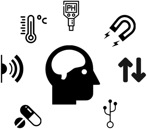
In we envisage the next functionalities that will be put on board of a neural interface starting from temperature, pressure and pH sensors arrays to more sophisticated chemical sensing platforms to monitor the production of neurotransmitters or to follow at cell level the activation of the different ion channels. The implementation of micro-coils into the flexible grid could reduce the issue related to tissue response for long-term implants, thus adopting magnetic stimulation instead of electrical one also reducing issues related to materials loss during stimulation. Moreover, ultra-flexible microfluidics could help in providing drug delivery system to offer personalized treatments in patients affected by chronic neurological diseases. Integration of infrared and optical source arrays could guarantee the monitoring of blood fluxes or a direct stimulation for neurons in optogenetic experiments. Finally, a reliable bidirectional interaction could allow natural control of specific parts of the body for patients with paralysis or peripheral nervous system damages or open futuristic scenarios to allow brain-to-brain connectivity or brain-to-machine interoperability.
Figure 6. Possible technologies to be integrated in a future neural interface: local temperature and pH sensing, magnetic stimulation, drug delivery embedded functionalities, infrared-based communication module, reliable bidirectional communication and even brain-to-brain connectivity. Flexible electronics represents a promising ally to make it possible.
7. Conclusions
Flexible electronics is rapidly evolving from an exotic technology used in lab to a reliable ally for manufacturing future neural interfaces. Many fabrication strategies can be pursued and different materials can be adopted depending by the applications. Neural interfaces can represent a winning platform to unveil the ultimate secrets lying in our heads, thus allowing a deep comprehension of the physical and biological phenomena and their correlation with human behaviours. Next generation of neural interfaces promises new functionalities paving the way to astonishing applications in neuro-rehabilitation and smart treatments of chronic neurological disorders.
Correction Statement
This article has been republished with minor changes. These changes do not impact the academic content of the article.
Acknowledgments
We thank Mr Ivano Lucarini and Mrs Claudia Bertozzi for their support in figures editing.
Disclosure statement
No potential conflict of interest was reported by the authors.
References
- Shulman RG. Brain imaging: what it can (and cannot) tell us about consciousness. Oxford : Oxford University Press; 2013.
- Teplan M. Fundamentals of eeg measurement. Meas Sci Rev. 2002;2:869–903.
- Dale AM, Liu AK, Fischl BR, et al. Neurotechnique-dynamic statistical parametric mapping: Combining fMRI and MEG for high-resolution imaging of cortical activity. Neuron. 2000;26:55–68.
- Fox PT, Burton H, Raichle ME. Mapping human somatosensory cortex with positron emission tomography. J Neurosurg. 1987;67:690–696.
- Buzsáki G, Stark E, Berényi A, et al. Tools for probing local circuits : high-density silicon probes combined with optogenetics. Neuron. 2015;86:92–105.
- Collinger JL, Wodlinger B, Downey JE, et al. High-performance neuroprosthetic control by an individual with tetraplegia. Lancet. 2013;381:557–564.
- Hochberg LR, Serruya MD, Friehs GM, et al. Neuronal ensemble control of prosthetic devices by a human with tetraplegia. Nature. 2006;442:164–171.
- Simeral JD, Kim SP, Black MJ, et al. Neural control of cursor trajectory and click by a human with tetraplegia 1000 days after implant of an intracortical microelectrode array. J Neural Eng. 2011;8(2):025027.
- Vansteensel MJ, Pels EGM, Bleichner MG, et al. Fully implanted brain-computer interface in a locked-in patient with ALS. N Engl J Med. 2016;375:2060–2066.
- Kim GH, Kim K, Lee E, et al. Recent progress on microelectrodes in neural interfaces. Materials. 2018;11:1995.
- Adly N, Weidlich S, Seyock S, et al. Printed microelectrode arrays on soft materials : from PDMS to hydrogels. Npj Flex Electron. 2018;1–9. DOI:10.1038/s41528-018-0027-z.
- Morin FO, Takamura Y, Tamiya E. Investigating neuronal activity with planar microelectrode arrays : achievements and new perspectives. J Biosci Bioeng. 2005;100:131–143.
- Chen N, Tian L, Patil AC, et al. Neural interfaces engineered via micro- and nanostructured coatings. Nano Today. 2017;14:59–83.
- Renz AF, Reichmuth AM, Stauffer F, et al. A guide towards long-term functional electrodes interfacing neuronal tissue. J Neural Eng. 2018;15:1–17.
- Khodagholy D, Gelinas JN, Thesen T, et al. NeuroGrid: recording action potentials from the surface of the brain. Nat Neurosci. 2015;18:310–315.
- Viventi J, Kim D-H, Vigeland L, et al. Flexible, foldable, actively multiplexed, high-density electrode array for mapping brain activity in vivo. Nat Neurosci. 2011;14:1599–1605.
- Mestre ALG, Inácio PMC, Elamine Y, et al. Extracellular electrophysiological measurements of cooperative signals in astrocytes populations. Front Neural Circuits. 2017;11:1–9.
- Wong WS, Alberto S. Flexible electronics materials and applications. Cambridge : Springer 2009.
- Brody TP. The thin film transistor-a late flowering bloom. IEEE Trans Electron Devices. 1984;31:1614–1628.
- Nomura K, Ohta H, Takagi A, et al. Room-temperature fabrication of transparent flexible thin-film transistors using amorphous oxide semiconductors. Nature. 2004;432:3383–3386.
- Zeng W, Shu L, Li Q, et al. Fiber-based wearable electronics: A review of materials, fabrication, devices, and applications. Adv Mater. 2014;26:5310–5336.
- Irimia-Vladu M, Głowacki ED, Voss G, et al. Green and biodegradable electronics. Mater Today. 2012;15:340–346.
- Ferrone A, Maita F, Maiolo L, et al. Wearable Band for Hand Gesture Recognition based on Strain Sensors. IEEE RAS & EMBS international conference on biomedical robotics and biomechatronics; 2016. p. 4–7. doi:10.1109/BIOROB.2016.7523814
- Stoppa M, Chiolerio A. Wearable electronics and smart textiles: A critical review. Sensors (Switzerland). 2014;14:11957–11992.
- Pecora A, Maiolo L, Cuscunà M, et al. Low-temperature polysilicon thin film transistors on polyimide substrates for electronics on plastic. Solid State Electron. 2008;52:348–352.
- Lu X, Xia Y. Electronic materials: buckling down for flexible electronics. Nat Nanotechnol. 2006;1:163–164.
- Artukovic E, Kaempgen M, Hecht DS, et al. Transparent and flexible carbon nanotube transistors. Nano Lett. 2005;5:757–760.
- Kim D, Song J, Choi WM, et al. Materials and noncoplanar mesh designs for integrated circuits with linear elastic responses to extreme mechanical deformations. Proc Nat Acad Sci. 2008;105:1–6.
- Ji B, Guo Z, Wang M, et al. Flexible polyimide-based hybrid opto-electric neural interface with 16 channels of micro-LEDs and electrodes. Microsyst Nanoeng. 2018;4.
- Stieglitz T, Beutel H, Schuettler M, et al. Micromachined, polyimide-based devices for flexible neural interfaces. Biomed Microdevices. 2000;2:283–294.
- Minev IR, Musienko P, Hirsch A, et al. Electronic dura mater for long-term multimodal neural interfaces. Science. 2015;347:159–164.
- Jang K, Chung HU, Xu S, et al. Soft network composite materials with deterministic and bioinspired designs. Nat Commun. 2015;6:1–11.
- Kaltenbrunner M, Sekitani T, Reeder J, et al. An ultra-lightweight design for imperceptible plastic electronics. Nature. 2013;499:458–463.
- Lodato S, Arlotta P. Generating neuronal diversity in the mammalian cerebral cortex. Annu Rev Cell Dev Biol. 2015;31:699–720.
- Mountcastle VB. Modality and topographic properties of single neurons of cat’s somatic sensory. J Neurophysiol. 1957;20:408–434.
- Jones EG. Microcolumns in the cerebral cortex. PNAS. 2000;97:5019–5021.
- Schevon CA, Ng SK, Cappell J, et al. Microphysiology of epileptiform activity in human neocortex. J Clin Neurophysiol. 2010;25:321–330.
- Takmakov P, Ruda K, Scott Phillips K, et al. Rapid evaluation of the durability of cortical neural implants using accelerated aging with reactive oxygen species. J Neural Eng. 2015;12:1–29.
- Wolf PD, Reichert WM. Thermal considerations for the design of an implanted cortical brain–machine interface (BMI). Indwelling Neural Implant. Strateg. Contend. with the In Vivo Environ; Boca Raton (FL): CRC Press/Taylor & Francis; 2008. Chapter 3. 2008. p. 33–38.
- IEEE SCC39. IEEE Std C95.1-2005 IEEE standard for safety levels with respect to human exposure to radio frequency electromagnetic fields, 3 kHz to 300 GHz. IEEE Std C95.1-2005 (Revision of IEEE Std C95.1-1991); IEEE. 2005.
- Lacour SP, Courtine G, Guck J. Materials and Technologies for soft implantable neuroprostheses. Nat Rev Mater. 2016;1.
- Kim D, Viventi J, Amsden JJ, et al. Dissolvable films of silk fibroin for ultrathin, conformal bio-integrated electronics. Nat Mater. 2010;9:511–517.
- Geddes LA, Hoff HE. The discovery of bioelectricity and current electricity the galvani-volta controversy. IEEE Spectr. 1971;8:38–46.
- Golgi C. Sulla struttura della sostanza grigia del cervello. Gazz Medica Ital. 1873;6:244–246.
- Ramón Y Cajal S. Textura del sistema nervioso del hombre y de los vertebrados : estudios sobre el plan estructural y composición histológica de los centros nerviosos adicionados de consideraciones fisiológicas fundadas en los nuevos descubrimientos. Madrid : N. Moya. 1894.
- Waldeyer-Hartz W. Ueber einige neuere Forschungen im Gebiete der Anatomie des Centralnervensystems. Leipzig : G. Tieme,1891.
- Hodgkin AL, Huxley F. Action potentials recorded from inside a nerve fibre. Nature. 1939;144:710–711.
- Frank BK, Fuortes MGF. Potentials recorded from the spinal cord with microelectrodes. J Physiol. 1955;130:625–654.
- Robinson DA. The electrical properties of metal microelectrodes. Proc IEEE. 1968;56:1065–1071.
- Thomas CA, Springer PA, Loeb GE, et al. A Miniature Microelectrode Array To Monitor The Bioelectric Activity Of Cultured Cells. Exp Cell Res. 1972;74:61–66.
- Pine J. Recording action potentials from cultured neurons with extracellular microcircuit electrodes. J Neurosci Methods. 1980;2:19–31.
- Gross GW. Simultaneous single unit recording in vitro with a photoetched laser deinsulated gold multimicroelectrode surface. IEEE Trans Biomed Eng. 1979;26:273–279.
- Shamma-donoghue SA, May GA, Cotter NE, et al. Thin-film multielectrode arrays for a cochlear prosthesis. IEEE Transactions on Electron Devices 1982;29;136–144 .
- Boppard SA, Wheeler BC, Wallace CS. A flexible perforated microelectrode array for extended neural recordings. IEEE Trans Biomed Eng. 1992;39:37–42.
- Hazrati MK, Husin HM, Hofmann UG Wireless brain signal recordings based on capacitive electrodes. 2013 IEEE 8th international symposium on intelligent signal Processing. WISP 2013 – proceedings; 2013. p. 8–13. doi:10.1109/WISP.2013.6657474
- Cogan SF, Plante TD, Ehrlich J Sputtered iridium oxide films (SIROFs) for low-impedance neural stimulation and recording electrodes. 26th annual international conference of the IEEE engineering in medicine and biology society; San Francisco CA 2005. Vol. 2, p. 4153–4156.
- Aqrawe Z, Montgomery J, Travas-Sejdic J, et al. Conducting Polymers for neuronal microelectrode array recording and stimulation. Sens Actuators B Chem. 2018;257:753–765.
- LeFloch F, Ho H-A, Harding-Lepage P, et al. Ferrocene‐functionalized cationic polythiophene for the label‐free electrochemical detection of DNA. Adv Mater. 2005;17:1251–1254.
- Castagnola E, Maiolo L, Maggiolini E, et al. Pedot-cnt-coated low-impedance, ultra-flexible, and brain-conformable micro-ECoG arrays. IEEE Trans Neural Syst Rehabil Eng. 2015;23:342–350.
- Castagnola V, Descamps E, Lecestre A, et al. Parylene-based flexible neural probes with PEDOT coated surface for brain stimulation and recording. Biosens Bioelectron. 2015;67:450–457.
- Cui X, Hetke JF, Wiler JA, et al. Electrochemical deposition and characterization of conducting polymer polypyrrole/PSS on multichannel neural probes. Sens Actuators A Phys. 2001;93:8–18.
- Marelli M, Divitini G, Collini C, et al. Flexible and biocompatible microelectrode arrays fabricated by supersonic cluster beam deposition on SU-8. J Micromech Microeng. 2011;21:045013.
- Corbelli G, Ghisleri C, Marelli M, et al. Highly deformable nanostructured elastomeric electrodes with improving conductivity upon cyclical stretching. Adv Mater. 2011;23:4504–4508.
- Chapman CAR, Chen H, Stamou M, et al. Nanoporous gold as a neural interface coating: effects of topography, surface chemistry, and feature size. ACS Appl Mater Interfaces. 2015;7:7093–7100.
- Boehler C, Stieglitz T, Asplund M. Nanostructured platinum grass enables superior impedance reduction for neural microelectrodes. Biomaterials. 2015;67:346–353.
- Kim KS, Zhao Y, Jang H, et al. Large-scale pattern growth of graphene films for stretchable transparent electrodes. Nature. 2009;457:706–710.
- David-Pur M, Bareket-Keren L, Beit-Yaakov G, et al. All-carbon-nanotube flexible multi-electrode array for neuronal recording and stimulation. Biomed Microdevices. 2014;16:43–53.
- Castagnola E, Ansaldo A, Maggiolini E, et al. Biologically compatible neural interface to safely couple nanocoated electrodes to the surface of the brain. ACS Nano. 2013;7:3887–3895.
- Cui X, Martin DC. Fuzzy gold electrodes for lowering impedance and improving adhesion with electrodeposited conducting polymer films. Sens Actuators A Phys. 2003;103:384–394.
- Brüggemann D, Wolfrum B, Maybeck V, et al. Nanostructured gold microelectrodes for extracellular recording from electrogenic cells. Nanotechnology. 2011;22:265104.
- Dankerl M, Eick S, Hofmann B, et al. Diamond transistor array for extracellular recording from electrogenic cells. Adv Funct Mater. 2009;19:2915–2923.
- Blaschke BM, Lottner M, Drieschner S, et al. Flexible graphene transistors for recording cell action potentials. 2D Mater. 2016;3:25007.
- Ojovan SV. A feasibility study of multi-site,intracellular recordings from mammalian neurons by extracellular gold mushroom-shaped microelectrodes. Sci Rep. 2015;5.
- Robinson JT, Jorgolli M, Shalek AK, et al. Vertical nanowire electrode arrays as a scalable platform for intracellular interfacing to neuronal circuits. Nat Nanotechnol. 2012;7:180.
- Xie C, Lin Z, Hanson L, et al. Intracellular recording of action potentials by nanopillar electroporation. Nat Nanotechnol. 2012;7:185.
- Qing Q, Jiang Z, Xu L, et al. Free-standing kinked nanowire transistor probes for targeted intracellular recording in three dimensions. Nat Nanotechnol. 2014;9:142.
- Suyatin DB, Wallman L, Thelin J, et al. Nanowire-based electrode for acute in vivo neural recordings in the brain. PLoS One. 2013;8:e56673.
- Castagnola E, Maggiolini E, Ceseracciu L, et al. pHEMA encapsulated PEDOT-PSS-CNT microsphere microelectrodes for recording single unit activity in the brain. Front Neurosci. 2016;10:1–14.
- Zhong Y, Bellamkonda RV. Dexamethasone-coated neural probes elicit attenuated inflammatory response and neuronal loss compared to uncoated neural probes. Brain Res. 2007;1148:15–27.
- Feiner R, Dvir T. Tissue–electronics interfaces: from implantable devices to engineered tissues. Nat Rev Mater. 3,17076 (2018).
- Pires F, Ferreira Q, Rodrigues CAV, et al. Neural stem cell differentiation by electrical stimulation using a cross-linked PEDOT substrate : expanding the use of biocompatible conjugated conductive polymers for neural tissue engineering. Biochim Biophys Acta. 2015;1850:1158–1168.
- Luo X, Weaver CL, Zhou DD, et al. Highly stable carbon nanotube doped poly (3, 4-ethylenedioxythiophene) for chronic neural stimulation. Biomaterials. 2011;32:5551–5557.
- Maiolo L, Polese D, Pecora A, et al. Highly disordered array of silicon nanowires: an effective and scalable approach for performing and flexible electrochemical biosensors. Adv Healthc Mater. 2016;5:575–583.
- Convertino A, Mussi V, Maiolo L. Disordered array of Au covered Silicon nanowires for SERS biosensing combined with electrochemical detection. Sci Rep. 2016;6:25099.
- Hanson L, Lin ZC, Xie C, et al. Characterization of the cell–nanopillar interface by transmission electron microscopy. Nano Lett. 2012;12:5815–5820.
- Persson H, Købler C, Mølhave K, et al. Fibroblasts cultured on nanowires exhibit low motility, impaired cell division, and DNA damage. Small. 2013;9:4006–4016.
- Liu J, Fu T-M, Cheng Z, et al. Syringe-injectable electronics. Nat Nanotechnol. 2015;10:629–636.
- Park D, Hamm JM, Page AF, et al. Graphene-based carbon-layered electrode array technology for neural imaging and optogenetic applications. Nat Commun. 2014;5:1–11.
- Qiang Y, Artoni P, Seo KJ, et al. Transparent arrays of bilayer-nanomesh microelectrodes for simultaneous electrophysiology and two-photon imaging in the brain. Sci. Adv.2018,4(9), eaat0626.
- Suo Z, Ma EY, Gleskova H, et al. Mechanics of rollable and foldable film-on-foil electronics. Appl Phys Lett. 1999;74:1177–1179.
- Fang H, Zhao J, Yu KJ, et al. Ultrathin, transferred layers of thermally grown silicon dioxide as biofluid barriers for biointegrated flexible electronic systems. 2016;113:11682–11687.
- Ferrone A Jiang X, Maiolo L, et al. A fabric-based wearable band for hand gesture recognition based on filament strain sensors: A preliminary investigation. in 2016 IEEE Healthcare Innovation Point-of-Care Technologies Conference, HI-POCT 2016; 2016. doi:10.1109/HIC.2016.7797710
- Liu J. Syringe injectable electronics. Biomimetics Through Nanoelectron. Springer Theses (Recognizing Outstanding Ph.D. Research). Springer, Cham 2017;65–93.
- Campbell PK, Jones KE, Huber RJ, et al. A silicon-based, three-dimensional neural interface: manufacturing processes for an intracortical electrode array. IEEE Trans Biomed Eng. 1991;38:758–768.
- Herwik S, Kisban S, Aarts AAA, et al. Fabrication technology for silicon-based microprobe arrays used in acute and sub-chronic neural recording. J Micromech Microeng. 2009;19:074008.
- Pazzini L, Polese D, Weinert JF, et al. An ultra-compact integrated system for brain activity recording and stimulation validated over cortical slow oscillations in vivo and in vitro. Sci Rep. 2018;8:1–13.
- Lu B, Yuk H, Lin S, et al. Pure PEDOT : PSS hydrogels. Nat Commun. 2019;10.
- Lee W, Kim D, Matsuhisa N, et al. Transparent, conformable, active multielectrode array using organic electrochemical transistors. PNAS. 2017;114.
- Won SM, Song E, Zhao J, et al. Recent advances in materials, devices, and systems for neural interfaces. Adv Mater. 2018;30:1–19.
- Angotzi GN, Boi F, Lecomte A, et al. SiNAPS: an implantable active pixel sensor CMOS-probe for simultaneous large-scale neural recordings. Biosens Bioelectron. 2019;126:355–364.
- Raducanu BC, Yazicioglu RF, Lopez CM, et al. Time multiplexed active neural probe with 1356 parallel recording sites. Sensors. 2017;17:1–20.
- Fortunato G, Pecora A, Maiolo L. Polysilicon thin-film transistors on polymer substrates. Mater Sci Semicond Process. 2012;15:627–641.
- Valletta A, Gaucci P, Mariucci L, et al. Role of gate oxide thickness in controlling short channel effects in polycrystalline silicon thin film transistors. Appl Phys Lett. 2009;95 033507.
- Privitera V, Scalese S, La Magna A, et al. Low-temperature annealing combined with laser crystallization for polycrystalline silicon TFTs on polymeric substrate. J Electrochem Soc. 2008;155:H764.
- Maiolo L, Pecora A, Maita F, et al. Flexible sensing systems based on polysilicon thin film transistors technology. Sensors Actuators B Chem. 2013;179:114–124.
- An S, Lee J, Kim Y, et al. 2. 8-Inch WQVGA flexible AMOLED using high performance low temperature polysilicon TFT on plastic substrates. Soc. Inf. Display(SID) Symp. Dig., 2010;2–6. DOI:10.1889/1.3500566.
- Kim CW Jung JG, Choi JB, et al. 59. 1 : invited Paper : LTPS backplane technologies for AMLCDs and AMOLEDs crystallization; 2011. p. 862–865
- Keren DM, Efrati A, Maita F, et al. Low temperature poly-silicon thin film transistor flexible sensing circuit. 2016 IEEE International Conference on the Science of Electrical Engineering (ICSEE) Eilat, Israel 2016;31–33.
- Fortunato G, Cuscuna M, Gaucci P, et al. Self-heating effects in p-channel polysilicon TFTs fabricated on different substrates. J Korean Phys Soc. 2009;54:455–463.
- Gaucci P, Valletta A, Mariucci L, et al. Analysis of self-heating-related instability in self-aligned p-channel polycrystalline-silicon thin-film transistors. IEEE Electron Device Lett. 2010;31:830–832.
- Maita F Maiolo L, Minotti A, et al. Flexible double stage POSTFT based on Poly-Si technology for robotic skin application. IEEE NANO 2015 15th international conference on nanotechnology; 2016. p. 1313–1316. doi:10.1109/NANO.2015.7388874
- Maiolo L, Mirabella S, Maita F, et al. Flexible pH sensors based on polysilicon thin film transistors and ZnO nanowalls. Appl Phys Lett. 2014;105:93501.
- Maita F, Maiolo L, Minotti A, et al. ultraflexible tactile piezoelectric sensor based on low-temperature polycrystalline silicon thin-film transistor technology. IEEE Sens J. 2015;15:3819–3826.
- Yu KJ, Kuzum D, Hwang SW, et al. Bioresorbable silicon electronics for transient spatiotemporal mapping of electrical activity from the cerebral cortex. Nature Materials 2016;15:782-791.
- Viventi J, Kim D-H, Vigeland L, et al. Flexible, foldable, actively multiplexed, high-density electrode array for mapping brain activity in vivo. Nat Neurosci. 2011;14:1599–1605.
- Christiaens W, Bosman E, Vanfleteren J. UTCP : a novel polyimide-based ultra-thin chip packaging technology. IEEE Transactions on Components and Packaging Technologies 2010;33:754–760.
- Van Den Brand J, de Kok M, Sridhar A, et al. Flexible and stretchable electronics for wearable healthcare. In 2014 44th European solid-state device research conference; Venice, Italy 2014. p. 206–209. doi:10.1109/ESSDERC.2014.6948796
- Rogers JA, Someya T, Huang Y. Materials and mechanics for stretchable electronics. Science. 2010;327:1603-1607.
- Fang H, Yu KJ, Gloschat C, et al. Capacitively coupled arrays of multiplexed flexible silicon transistors for long-term cardiac electrophysiology. Nat Biomed Eng. 2017;1–23. DOI:10.1038/s41551-017-0038.Capacitively.
- Someya T. Building bionic skin. IEEE Spectr. 2013;50:50–56.
- Yeo W-H, Kim Y-S, Lee J, et al. Multifunctional epidermal electronics printed directly onto the skin. Adv Mater. 2013;25:2773–2778.
- Nomura K, Ohta H, Ueda K, et al. Thin-film transistor fabricated in single-crystalline transparent oxide semiconductor. Science. 2003;300:1269–1272.
- Fortunato E, Barquinha P, Pimentel A, et al. Recent advances in ZnO transparent thin film transistors. Thin Solid Films. 2005;487:205–211.
- Fortunato EM, Pereira LM, Barquinha PM et al. High mobility indium free amorphous oxide thin film transistors. Appl Phys Lett. 2008;92:222103.
- Carcia PF, McLean RS, Reilly MH, et al. Transparent ZnO thin-film transistor fabricated by rf magnetron sputtering. Appl Phys Lett. 2003;82:1117–1119.
- Ju S, Facchetti A, Xuan Y, et al. Fabrication of fully transparent nanowire transistors for transparent and flexible electronics. Nat Nanotechnol. 2007;2:378–384.
- Adamopoulos G, Bashir A, Gillin WP, et al. Structural and electrical characterization of ZnO films grown by spray pyrolysis and their application in thin-film transistors. Adv Funct Mater. 2011;21:525–531.
- Bashir A, Wöbkenberg PH, Smith J, et al. High-performance zinc oxide transistors and circuits fabricated by spray pyrolysis in ambient atmosphere. Adv Mater. 2009;21:2226–2231.
- Dai MK, Lian JT, Lin TY, et al. High-performance transparent and flexible inorganic thin film transistors: A facile integration of graphene nanosheets and amorphous InGaZnO. J Mater Chem C. 2013;1:5064–5071.
- Prins MWJ, Grosse‐Holz K-O, Müller G, et al. A ferroelectric transparent thin-film transistor. Appl Phys Lett. 1996;68:3650–3652.
- Seager CH, McIntyre DC, Warren WL, et al. Charge trapping and device behavior in ferroelectric memories. Appl Phys Lett. 1995;2660:2660.
- Petti L, Münzenrieder N, Vogt C, et al. Metal oxide semiconductor thin-film transistors for flexible electronics. Appl Phys Rev. 2016;3:021303.
- Yu X, Marks TJ, Facchetti A. Metal oxides for optoelectronic applications. Nat Mater. 2016;15:383–396.
- Kim JB, Fuentes-Hernandez C, Hwang DK, et al. Vertically stacked hybrid organic-inorganic complementary inverters with low operating voltage on flexible substrates. Org Electron Phys Mater Appl. 2011;12:45–50.
- Oh MS, Choi W, Lee K, et al. Flexible high gain complementary inverter using n-ZnO and p -pentacene channels on polyethersulfone substrate. Appl Phys Lett. 2008;93:1–4.
- Honda W, Harada S, Ishida S, et al. High-performance, mechanically flexible, and vertically integrated 3D carbon nanotube and InGaZnO complementary circuits with a temperature sensor. Adv Mater. 2015;27:4674–4680.
- Barquinha P, Fortunato E, Gonçalves A, et al. Influence of time, light and temperature on the electrical properties of zinc oxide TFTs. Superlattices Microstruct. 2006;39:319–327.
- Fortunato E, Barquinha P, Martins R. Oxide semiconductor thin-film transistors: A review of recent advances. Adv Mater. 2012;24:2945–2986.
- Someya T, Bao Z, Malliaras GG. The rise of plastic bioelectronics. Nature. 2016;540:379–385.
- Castagnola E, Maiolo L, Maggiolini E, et al. PEDOT-CNT-coated low-impedance, ultra-flexible, and brain-conformable micro-ECoG arrays. IEEE Trans Neural Syst Rehabil Eng. 2014;23:342–350.
- Castagnola E Maiolo L, Maggiolini E, et al. Ultra-flexible and brain-conformable micro-electrocorticography device with low impedance PEDOT-carbon nanotube coated microelectrodes. International IEEE EMBS conference on neural engineering. NER;San Diego, CA 2013. p. 927–930. doi:10.1109/NER.2013.6696087
- Castagnola E, Marrani M, Maggiolini E, et al. Recording high frequency neural signals using conformable and low-impedance ECoG electrodes arrays coated with PEDOT-PSS-PEG. In Advances in Science and Technology (Vol. 102, pp. 77-85). Trans Tech Publications.
- Simeone D, Cipolloni S, Mariucci L, et al. Pentacene TFTs with parylene passivation layer. Thin Solid Films. 2009;517:6283–6286.
- Mariucci L, Simeone D, Cipolloni S, et al. Effect of active layer thickness on electrical characteristics of pentacene TFTs with PMMA buffer layer. Solid State Electron. 2008;52:412–416.
- Someya T, Sekitani T, Iba S, et al. A large-area, flexible pressure sensor matrix with organic field-effect transistors for artificial skin applications. Proc Natl Acad Sci. 2004;101:9966–9970.
- Katz H, Kato Y, Sekitani T, et al. Conformable, flexible, large-area networks of pressure and thermal sensors with organic transistor active matrixes. Proc Natl Acad Sci. 2002;98:4835–4840.
- Khan S, Lorenzelli L, Dahiya RS. Technologies for printing sensors and electronics over large flexible substrates: A review. IEEE Sens J. 2015;15:3164–3185.
- Benight SJ, Wang C, Tok JBH, et al. Stretchable and self-healing polymers and devices for electronic skin. Prog Polym Sci. 2013;38:1961–1977.
- Reese C, Roberts M, Ling M, et al. Organic thin-film transistors. Mater Today. 2004;7:28–35.
- Lago N, Cester A. Flexible and organic neural interfaces: a review. Appl Sci. 2017;7(12)1292.
- Khodagholy D, Doublet T, Quilichini P, et al. In vivo recordings of brain activity using organic transistors. Nat Commun. 2013;4:1575.
- Drack M, Graz I, Sekitani T, et al. An imperceptible plastic electronic wrap. Adv Mater. 2014;27:34–40.
- Ng KA, Greenwald E, Xu YP, et al. Implantable neurotechnologies: a review of integrated circuit neural amplifiers. Med Biol Eng Comput. 2016;54:45–62.
- Hong JH Liang, MC, Haung MY, et al. Analog front-end circuit with low-noise amplifier and high-pass sigma-delta modulator for an EEG or ECoG acquisition system. Proceedings - 2014 IEEE international conference on bioinformatics, ISBB 2011; 2011. p. 17–20. doi:10.1109/ISBB.2011.6107634
- Robinet S, Audebert P, Regis G, et al. A low-power 0.7 μv rms 32-channel mixed-signal circuit for ECoG recordings. IEEE J Emerg Sel Top Circuits Syst. 2011;1:451–460.
- Gao H, Walker RM, Nuyujukian P, et al. HermesE: A 96-channel full data rate direct neural interface in 0.13 μm CMOS. IEEE J Solid-State Circuits. 2012;47:1043–1055.
- Cheng CH, Chen ZX, Wu CY A 16-channel CMOS chopper-stabilized analog front-end acquisition circuits for ECoG detection. proceedings - IEEE International Symposium on Circuits and Systems; Baltimore, MD 2017. p. 4–7. doi:10.1109/ISCAS.2017.8050954
- Chang CW, Chiou JC, A Wireless and batteryless microsystem with implantable grid electrode/3-dimensional probe array for ECoG and extracellular neural recording in rats. Sensors, 2013;4624–4639. DOI:10.3390/s130404624.
- Matsushita K, Hirata M, Suzuki T, et al. A fully implantable wireless ECoG 128-channel recording device for human brain – machine interfaces. Front Neurosci. 2018;12:1–11.
- Mestais CS, Charvet G, Sauter-starace F, et al. WIMAGINE : wireless 64-channel ECoG recording implant for long term clinical applications. IEEE Trans Neural Syst Rehabil Eng. 2015;23:10–21.
- Karimi-bidhendi A, Malekzadeh-Arasteh O, Lee MC, et al. CMOS ultralow power brain signal acquisition front-ends : design and human testing. IEEE Transactions on Biomedical Circuits and Systems. 2017;11:1111–1122.
- Polese D, Pazzini L, Delgado-Martínez I, et al. An ultra-compact low-powered closed-loop device for control of the neuromuscular system. In International Conference on Artificial Neural Networks. Cham: Springer;. 2017. p. 60-67.
- Kassiri H, Tonekaboni S, Salam MT, et al. Closed-loop neurostimulators: a survey and a seizure-predicting design example for intractable epilepsy treatment. IEEE Trans Biomed Circuits Syst. 2017;11:1026–1040.
- Liu X, Zhang M, Xiong T, et al. A fully integrated wireless compressed sensing neural signal acquisition system for chronic recording and brain machine interface. IEEE Trans Biomed Circuits Syst. 2016;10:874–883.
- Lee B, Jia Y, Mirbozorgi SA, et al. An inductively powered wireless neural recording and stimulation system for freely-behaving animals. IEEE Trans Biomed Circuits Syst. 2019;13:1.
- Chan YC, Luk DY. Effects of bonding parameters on the reliability performance of anisotropic conductive adhesive interconnects for flip-chip-on-flex packages assembly I. Different bonding temperature. Microelectron Reliab. 2002;42:1185–1194.
- Li M, Wu Y, Zhang L, et al. Liquid metal-based electrical interconnects and interfaces with excellent stability and reliability for flexible electronics. Nanoscale. 2019;11:5441–5449.
- Dang W, Vinciguerra V, Lorenzelli L, et al. Printable stretchable interconnects. Flex Print Electron. 2017;2:013003.
- Karandrea A, Invasive and non-invasive neural interfaces: forecasts and applications 2018–2028. IDtechex. 2018.
- Schwarz DA, Lebedev MA, Hanson TL, et al. Chronic, wireless recordings of large-scale brain activity in freely moving rhesus monkeys. Nat Methods. 2014;11:670–676.
- Borton DA, Yin M, Aceros J, et al. An implantable wireless neural interface for recording cortical circuit dynamics in moving primates. J Neural Eng. 2013;10:026010.
- Yin M, Borton DA, Komar J, et al. Wireless neurosensor for full-spectrum electrophysiology recordings during free behavior. Neuron. 2014.17;84(6):1170-82 DOI:10.1016/j.neuron.2014.11.010
- Hochberg LR, Bacher D, Jarosiewicz B, et al. Reach and grasp by people with tetraplegia using a neurally controlled robotic arm. Nature. 2012;485:213–216.
- Nuyujukian P, Albites Sanabria J, Saab J, et al. Cortical control of a tablet computer by people with paralysis. PLoS One. 2018;13:1–16.
- Shin G, Gomez AM, Al-Hasani R, et al. Flexible near-field wireless optoelectronics as subdermal implants for broad applications in optogenetics. Neuron. 2017;93(3):509-521.
- Mendes PM. Cellular nanotechnology : making biological interfaces smarter. Chem Soc Rev. 2013;42:9207–9218.
- Nguyen-Vu TDB, Chen H, Cassell AM, et al. Vertically aligned carbon nanofiber architecture as a multifunctional 3-D neural electrical interface. IEEE Trans Biomed Eng. 2007;54:1121–1128.
- Liu X, Wang S. Three-dimensional nano-biointerface as a new platform for guiding cell fate. Chem Soc Rev. 2014;43:2385–2401.
- Novellino A, D’Angelo P, Cozzi L, et al. Connecting neurons to a mobile robot: an in vitro bidirectional neural interface. Comput Intell Neurosci. 2007;2007:1–13.
- Saracino E. Silicon Nanowire and Electrospun Nanofibre Polymer Interfaces and Devices to Alter Non Excitable Brain Cell Morphology and Functionality. in MRS fall meeting (2018); Boston, MA 2018.
- Sanchez-Vives MV, McCormick DA. Cellular and network mechanisms of rhythmic recurrent activity in neocortex. Nat Neurosci. 2000;3:1027–1034.
- Neely RM, Piech DK, Santacruz SR, et al. Recent advances in neural dust: towards a neural interface platform.. Curr Opin Neurobiol. 2018;50:64–71.