
 ?Mathematical formulae have been encoded as MathML and are displayed in this HTML version using MathJax in order to improve their display. Uncheck the box to turn MathJax off. This feature requires Javascript. Click on a formula to zoom.
ABSTRACT
Bismuth halogenides, a family of quasi-one-dimensional (1D) materials, including α and α phases of Bi4Br4 and Bi4I4, have been predicted to exhibit rich and interesting topological properties. The single layer of Bi4Br4 was demonstrated to be a quantum spin Hall insulator (QSHI) with a 0.18 eV gap. Such a band gap is large enough for the observation of QSHI at room temperature. Bulk α-Bi4Br4 was categorized as a higher-order topological insulator and was soon examined in experiments. In addition, the α-Bi4Br4 exhibit simultaneously the topological phase and superconductive phase under 3.8–4.3 GPa pressure. While the single layer of Bi4I4 was shown to be close to the critical point of the QSHI/trivial-insulator phase transition, the α-Bi4I4 was considered to be a strong or weak topological insulator. In this work, we reviewed the recent progress in the topological properties of bismuth halogenides, including the theoretical calculations, angle-resolved photoemission spectroscopy, scanned tunneling microscopy analyses, quantum transport measurement and the superconducting phase transfer under pressure. We expect further research of this family material about the non-trivial superconductor and possible Majorana, room-temperature quantum transport effect and potential application in the quantum device for the electronics and information technology.
Graphical Abstract
1. Introduction
Topological insulators host time-reversal-symmetry-protected spin-momentum-locked boundary states with linear energy dispersion, offering new opportunities for unprecedented advances in technologies, e.g. spintronics, microelectronics and infrared sensors [Citation1–10]. The strong and weak topological insulators (TI) were predicted and characterized by four Z2 invariants [Citation3,Citation4]. The hallmark of strong TIs is that every surface possesses a gapless Dirac cone, while that of weak TIs is that only selected surfaces have the nontrivial surface states [Citation11–30]. The two-dimensional topological insulators (also known as quantum spin Hall insulators) host robustly dissipationless conducting channels at the edge states [Citation31–40]. Recently, the higher-order TI is predicated to host protected gapless states on boundaries of two or three spatial dimensions lower than its bulk, which can be characterized by Z4 invariants [Citation41–50]. Furthermore, the topological phase transition between different topological phases can be induced by strain, thermal effects and extra-fields [Citation51–60]. All of those predictions require a suitable material platform for the research on topological physics. The family of bismuth halogenides, including α-Bi4Br4 and α-Bi4I4, has recently been attracting great interest, and various novel properties have been reported, e.g. strong topological insulator [Citation61], weak topological insulator [Citation62–64], high-order topological insulator [Citation65–68], superconductivity [Citation69–73] and quantum spin Hall effect for single layer [Citation74–78].
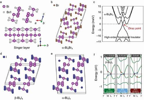
Bismuth halogenides, a new family of topological materials, are composed of one-dimensional (1D) chains (Bi4X4). The coupling between neighboring chains is rather weak and comparable with the interlayer coupling. Such a special structure features Bi4X4 as quasi-1D materials. Particularly, the single-layer Bi4Br4, an in-plane close-packing of parallel Bi4Br4 chains, was identified as a quantum spin Hall insulator (QSHI) that hosts gapless helical edge states [Citation74–77]. Bulk α-Bi4Br4, built from the van der Waals stacking of double layers with one of them flipped by 180° in the unit cell, was categorized as a higher-order topological insulator (HOTI) [Citation65–68] and has recently been examined by using angle-resolved photoemission spectroscopy (ARPES) [Citation65]. As the coupling of the topological edge states localized in different Bi4Br4 layers is relatively weak, the edge states of α-Bi4Br4 always maintain their 1D nature, regardless of the numbers of the stacked layers [Citation75]. Such 1D topological edge states at the step edges of α-Bi4Br4 have also been confirmed by scanned tunneling microscopy (STM) [Citation66,Citation76,Citation77]. α-Bi4Br4 with AA stacking was predicted to be a weak topological insulator (WTI) based on the first-principle calculation [Citation62]. Similarly, α-Bi4I4 was also considered to be a WTI and analyzed by ARPES [Citation63]. Though Liu and coworkers predicted α-Bi4I4 as a strong topological insulator (STI), they also indicated α-Bi4I4 as a WTI with a tiny strain [Citation62]. Therefore, the topology of β-Bi4I4 is still in controversy and needs careful examination. Under the pressure, bismuth halogenides can transform to superconducting phases, leading to possible topological superconductors [Citation69–73]. The pioneering works have been attracting great research interest on the family of bismuth halogenides, including α/β-Bi4Br4 and α/β-Bi4I4 due to their various exotic properties. It is worth reviewing recent reports about the material family of bismuth halogenides. The novel physics for these materials is valued for future exploration. In this review, section 2 introduces the crystal structure of bismuth halogenides; section 3 gives the theoretical calculation of the electronic structures; section 4 shows the ARPES results to verify the topologies of Bi4Br4 and Bi4I4; section 5 shows the edge states observed by the STM; section 6 and 7 discuss the quantum transport properties without and with pressure.
2. Crystal structures of and β phases of Bi4X4(X = Br,I)
2.1 Single-layer Bi4X4(X = Br,I)
Quasi-one-dimensional material Bi4X4(X = Br,I) was built up by a one-dimensional (1D) infinite molecular chain. As shown in , in one molecular chain, the one-unit cell consists of four Br/I atoms and four Bi atoms. Among four Bi atoms, the two internal Bi atoms (Biin) form zigzag atomic chains with strongly covalent Biin − Biin bonds (the nearest neighbor distance of 3.04 Å). The two external Bi atoms (Biex) are bonded to four halide atoms (the Bi-I distance of ∼3.14 Å and the Bi-Br distance of ∼2.9 Å) and to one internal Bi atom (the Biin − Biex distance of ∼3.06 Å) [Citation74]. The Biin − Biin and Biin − Biex bonds are nearly perpendicular to each other (∼ 91°). Then, the molecule chains are combined as a parallel arrangement to form a single layer of Bi4X4. From the top view, the single-layer structure belongs to the centered rectangular lattice. With such 1D infinite molecular chains as its building blocks, it could be naturally torn to nanoribbons with clean and atomically sharp edges. Zhou et al. calculated the binding energy of the chains in the single layers. The obtained value of interlayer binding energy (∼20 meV/Å2 or 70 meV/atom) is in the typical range for the vdW layered compound, which is comparable to the experimental result of graphite (∼12 meV/Å2) and MoS2 (∼26 meV/Å2) [Citation74]. In addition, the calculated binding energy between 1D chains within the single-layer Bi4Br4 (∼87 meV/atom) is larger than the interlayer binding energy. Therefore, exfoliation from the bulk should be a possible way to fabricate single- or few-layer Bi4Br4 nanoribbons. Furthermore, the dynamic stability of single-layer Bi4Br4 is confirmed through the phonon spectrum calculations. Though no similar calculation of Bi4I4 about the bonding energy and phonon spectrum of a few layers was reported, Bi4I4 is estimated to have similar mechanical properties as Bi4Br4.
Figure 1. Crystal structure of Bi4X4 (X = Br or I). a, crystal structure of a Bi4X4 1D chain. the gray balls and the pink balls are Br/I and Bi atoms, respectively. b-d, crystal structures of α-Bi4Br4 (b), β-Bi4I4 (c) and α-Bi4I4 (d) viewed from the chain direction (b direction). The brown balls and the blue balls are Br and I atoms, respectively. Figures reproduced from: (a) ref [Citation74], copyright 2014, American Chemical Society; (b,c,d) ref [Citation65] copyright 2021, Nature Publishing Group. β.
![Figure 1. Crystal structure of Bi4X4 (X = Br or I). a, crystal structure of a Bi4X4 1D chain. the gray balls and the pink balls are Br/I and Bi atoms, respectively. b-d, crystal structures of α-Bi4Br4 (b), β-Bi4I4 (c) and α-Bi4I4 (d) viewed from the chain direction (b direction). The brown balls and the blue balls are Br and I atoms, respectively. Figures reproduced from: (a) ref [Citation74], copyright 2014, American Chemical Society; (b,c,d) ref [Citation65] copyright 2021, Nature Publishing Group. β.](/cms/asset/e49fea6f-85ae-4e81-a096-dd90e2d4b2cc/tapx_a_2057234_f0001_oc.jpg)
2.2 Bulk Bi4X4(X = Br,I)
According to the theoretical calculations, both Bi4I4 and Bi4Br4 bulks have stable α and β phases [Citation62]. The two phases crystallize in the same monoclinic space group (C2/m) and vary from the differing stacking of 2D layer. The β phase is considered to be AA stacking. The lattice parameters of β-Bi4I4 are a = 14.386 Å, b = 4.430 Å, c = 10.493 Å and β = 107.9◦, respectively () [Citation61,Citation63,Citation64,Citation79–81]. No β-Bi4Br4 was reported by experiments. The stacking of α phases of Bi4I4 and Bi4Br4 is quite different. The α-Bi4Br4 can be regarded as a combined packing of the bottom layer and the top layer flipped by 180° in each unit cell (AB-stacking) as shown in . The interactions between adjacent single layers are of weak vdW-type. The lattice parameters of α-Bi4Br4 are a = 13.058 Å, b = 4.329 Å, c = 20.059 Å and β = 107.4◦, respectively [Citation62,Citation65–69,Citation75–77,Citation79–81]. In , the α-Bi4I4 takes a double-layered AA′-stacking structure. The top and the bottom layers have the same arrangement and direction. The top layer shifts b/2 distance along b axis compared with the bottom layer. The lattice parameters of α-Bi4I4 are a = 14.213 Å, b = 4.423 Å, c = 19.939 Å, and β = 92.91◦, respectively [Citation62–64,Citation82,Citation83]. In addition, the β phase of Bi4I4 was considered to easily transform to α phases in the sample cooling process from growth temperature to room temperature. Through rapid quenching from about 400 K to the temperature of liquid nitrogen (77 K), the structural transition from the β-phase to the α-phase could be suppressed; it was thereby possible to characterize the β-phase at low temperatures through resistivity and ARPES measurements [Citation63,Citation64,Citation83]. These two phases could be distinguished by the X-ray diffraction patterns from the ab plane due to the ab-plane spacing of the α phase close to twice that of the β phase [Citation61,Citation64,Citation82]. Therefore, the weak odd (00 l) (l = 2 n + 1) reflections can be used to distinguish the two phases in real experiments.
3. Electronic structures of single layer and bulk (α and β phases of Bi4X4(X = Br,I))
3.1 Bi4Br4
Single-layer Bi4Br4 was predicted to be a QSHI with a 0.18 eV gap () [Citation74,Citation84]. According to the first-principle calculation, both valence and conduction bands near the Fermi level are mainly constituted by Bi-6p orbitals [Citation65,Citation74]. As shown in , in the absence of spin-orbit coupling (SOC), the valence band maximum (VBM) is dominated by the Biin-px orbital with negative parity, while the conduction band minimum (CBM) is dominated by the Biex-px orbital with positive parity. The orbital has higher energy due to the much stronger σ-type hopping between
and
compared to the π-type of
. The Br-4p orbitals stay deep below the Fermi level due to the much larger electronegativity of bromine. Therefore, the
and
orbitals at Γ point have different parities under mirror operation with mirror plane parallel to the xz plane, leading them not to mix with each other without SOC. Furthermore, under inversion operation, the two Biin (Biex) atoms interchange site with each other. Orbitals from these two atoms can be combined to form bonding and antibonding states with split levels. The calculated band structure without SOC shows a direct band gap located at the Γ point. Generally, the GGA method is not an accurate method to calculate the band gap and gives a smaller value than the real value. With SOC, both the orbital character and the parity of CBM and VBM are inverted. That leads to a larger estimation of the band gap, ∼0.35 eV. To get a more accurate value of the band gap, we used the hybrid functional method (HSE06) and obtain a bandgap of ∼0.18 eV [Citation74]. To analyze the band topology, the Z2 topological invariant was calculated within the first-principle framework [Citation65,Citation74]. The result of Z2 = 1 verifies that single-layer Bi4Br4 is a QSHI. The gapless helical edge states inside the bulk band gap are the hallmark of QSHIs. The Fermi velocity of edge states in single-layer Bi4Br4 is ∼4.8 × 10⁵ m/s, which is slightly smaller than that of 5.5 × 10⁵ m/s in HgTe/CdTe quantum wells but is remarkably larger than that of 3 × 10⁴ m/s in InAs/GaSb quantum wells [Citation74]. This high Fermi velocity is beneficial to the fabrication of high-speed spintronics devices.
Figure 2. a, The edge density of states (first row) and spin polarization (second row) for single-layer, double-layer, and triple-layer Bi4Br4. The Fermi level is set to the bulk band gap center. b, At the stair-stepped edge, single-Dirac-cone edge states from the two different layers are degenerate, thus are decoupled in real space. c, Schematic diagram of the band evolution. The explanation is shown in the main text. Schematic figure (right corner) of the single-layer Bi4Br4 structure with Br atoms neglected. The filled and empty circles stand for Bi atoms from adjacent chains. The solid lines denote strong intrachain bonds, the dash lines denote weak interchain coupling. d, e, f, The bulk electronic band structures of α-Bi4Br4 and β-Bi4Br4, where SOC are included and HSE are employed. The symbols + and – label the parity eigenvalues of the band edges at L and M points. The dashed lines indicate Fermi levels. A band gap is opened for α-Bi4Br4 in d, whereas gapless topological hinge states emerge for α-Bi4Br4 in e; the Dirac point is indicated by the red arrow. β-Bi4Br4 is a WTI with (0;001) invariants and a 32 meV indirect gap. The (100) surface states exhibit two anisotropy surface Dirac cones with the absence of dangling bond states. g, h, i, The bulk band structures for α-Bi4I4 and β-Bi4I4 with the SOC. The dashed lines are the Fermi levels. A band gap is opened for α-Bi4I4 in g. β-Bi4I4 is an STI with (1;110) invariants and a 39 meV indirect gap with one highly anisotropic surface Dirac cone at the (001) cleavage surface in h. In i, the red and blue circles label respectively the even parities and odd parities for the bulk bands at the M and L points. The gap size was adjusted by varying the parameters in mBJ. The Z2 invariants cannot be confidently determined from theory alone, given that β-Bi4I4 is in proximity to three different phases, namely an STI (1;110), a WTI (0;001), or even a normal insulator (0;000), all of which are found within a small range of bandgap variation beyond the accuracy of theoretical calculations. Figure reproduced from (a,b) ref [Citation75] copyright 2015, Institute of Physics; (c) ref [Citation74] copyright 2014, American Chemical Society; (d,f,g,h) ref [Citation62] copyright 2014, American Physical Society; (e) ref [Citation65] copyright 2021, Nature Publishing Group; (i) ref [Citation63] copyright 2019, Nature Publishing Group.
![Figure 2. a, The edge density of states (first row) and spin polarization (second row) for single-layer, double-layer, and triple-layer Bi4Br4. The Fermi level is set to the bulk band gap center. b, At the stair-stepped edge, single-Dirac-cone edge states from the two different layers are degenerate, thus are decoupled in real space. c, Schematic diagram of the band evolution. The explanation is shown in the main text. Schematic figure (right corner) of the single-layer Bi4Br4 structure with Br atoms neglected. The filled and empty circles stand for Bi atoms from adjacent chains. The solid lines denote strong intrachain bonds, the dash lines denote weak interchain coupling. d, e, f, The bulk electronic band structures of α-Bi4Br4 and β-Bi4Br4, where SOC are included and HSE are employed. The symbols + and – label the parity eigenvalues of the band edges at L and M points. The dashed lines indicate Fermi levels. A band gap is opened for α-Bi4Br4 in d, whereas gapless topological hinge states emerge for α-Bi4Br4 in e; the Dirac point is indicated by the red arrow. β-Bi4Br4 is a WTI with (0;001) invariants and a 32 meV indirect gap. The (100) surface states exhibit two anisotropy surface Dirac cones with the absence of dangling bond states. g, h, i, The bulk band structures for α-Bi4I4 and β-Bi4I4 with the SOC. The dashed lines are the Fermi levels. A band gap is opened for α-Bi4I4 in g. β-Bi4I4 is an STI with (1;110) invariants and a 39 meV indirect gap with one highly anisotropic surface Dirac cone at the (001) cleavage surface in h. In i, the red and blue circles label respectively the even parities and odd parities for the bulk bands at the M and L points. The gap size was adjusted by varying the parameters in mBJ. The Z2 invariants cannot be confidently determined from theory alone, given that β-Bi4I4 is in proximity to three different phases, namely an STI (1;110), a WTI (0;001), or even a normal insulator (0;000), all of which are found within a small range of bandgap variation beyond the accuracy of theoretical calculations. Figure reproduced from (a,b) ref [Citation75] copyright 2015, Institute of Physics; (c) ref [Citation74] copyright 2014, American Chemical Society; (d,f,g,h) ref [Citation62] copyright 2014, American Physical Society; (e) ref [Citation65] copyright 2021, Nature Publishing Group; (i) ref [Citation63] copyright 2019, Nature Publishing Group.](/cms/asset/16059088-a03d-4653-b13d-4483038d00ec/tapx_a_2057234_f0002_oc.jpg)
As shown in , for bilayer Bi4Br4 with AB stacking as described above, two pairs of topological edge states are weakly coupled, resulting in a small gap opening of ∼20 meV [Citation75]. The gapped edge states indicate topological trivial phase in bilayer Bi4Br4. For trilayer Bi4Br4, three pairs of topological edge states are coupled. However, one pair of edge states crosses the band gap without gap opening, which indicates topological non-trivial phase in trilayer Bi4Br4. The difference in topology is due to the multilayer Bi4Br4 with an even (odd) number of layers having even (odd) times of band inversions. The even times of band inversions result in a trivial insulator with Ζ2 = 0, while odd times of band inversions result in a QSHI with Ζ2 = 1. Compared to the freestanding bilayer, the topological edge states from the two different layers are fully decoupled with a step width of ∼5 nm (). Fermi velocity of the decoupled edge states is a little smaller than that of the freestanding single-layer Bi4Br4.
Usually, when the single layers are stacked together to form bulk materials, the band gap will be reduced due to the interlayer orbital hopping. However, the interlayer coupling of Bi4X4 is rather weak and the band edges are all dominated by the in-plane orbitals; therefore, the inverted band gap of bulk with AB stacking (∼0.15 eV) is only reduced by ∼30 meV according to the HSE06 calculations () [Citation75]. In addition, the interlayer coupling of two layers in a one-unit cell leads to the opening of a tiny gap of ~ 20 meV of edge states. Therefore, α-Bi4Br4 is considered to be a trivial insulator, which (100)-oriented facet possesses surface states with a tiny band gap near the point. In 2019, Tang et al. used symmetry indicators to search for new topological materials [Citation41]. According to their theory, C2-rotation protected topological crystalline insulator Bi4Br4 was categorized as a higher-order topological insulator and expected to host 1D helical hinge states between the top surface (001) and the side surface (100) due to the second-order bulk–boundary correspondence () [Citation65–68]. For bulk Bi4Br4 with AA stacking (β phase), it has similar band inversions at both M and L points. According to Z2 topology, β-Bi4Br4 is a weak topological insulator with (0;001) invariants and a 32 meV indirect gap as shown in [Citation62].
and
are two distinct points at (100) surface projected by M and L point. At
and
, two highly anisotropic Dirac cones are observed with different energies since the surface is parallel to the atomic chains and exhibit prominent anisotropic surface states.
3.2 Bi4I4
For single-layer Bi4I4, it was shown to be close to the critical point of QSHI/trivial-insulator phase transition [Citation64,Citation74,Citation78]. Hence, the application of external strain can effectively tune the band structure and the topological phase of single-layer Bi4I4.
For bulk Bi4I4, the α-phase belongs to a kind of normal insulators (). The β phase might be a weak or strong topological insulator, depending on the details of the electronic structures. According to the first-principle calculations, β-Bi4I4 is an STI with (1;110) invariants and a 39 meV indirect gap with the VBM at the Γ point and the CBM at the M point () [Citation61,Citation62]. One surface Dirac cone at the (001) surface is located at the M point, different from that at the Γ point in most TIs. The band dispersion is relatively weak along the AΓYM path, which corresponds to the inter-chain bonding directions and strong along the BΓ direction-oriented parallel to the chains [Citation61]. The Fermi velocity of the Dirac fermion along the chain (νFy = 0.57 ×10⁶ m s−1) is over five times larger than that in the perpendicular direction (νFx = 0.10 ×10⁶ m s−1). Such a strong anisotropy of the surface-state Dirac fermions is caused by the quasi-1D structure of β-Bi4I4. However, Noguchi et al. suggested that β-Bi4I4 would be a weak TI with the Z2 indices (0;001) [Citation63]. The topological non-triviality of this material stems from the spin-orbit induced band inversion at the M and L points shown in . According to the topological theory, there are no topological surface states present at the (001) surface. In contrast, the (100) surface hosts topological states with a characteristic Dirac ‘groove’ dispersion.
4. Evidence of strong, weak or high-order topological insulators based on Angle-resolved photoemission spectroscopy spectra
4.1. β-Bi4I4, strong topological insulator
Aut s used ARPES to analyze the exposed (001) surface of β-Bi4I4 as shown in [Citation61]. By extracting the quasiparticle energies of the valence and conduction bands, a band gap of 50 meV can be estimated. At the
point, they reported a prominent
-shaped feature representing a crossing of nearly linearly dispersing bands, alongside parabolic bands at the
and
points of the surface Brillouin zone. Such band crossing in the small band gap of β-Bi4I4 is predicted to host topologically non-trivial states. The position of the crossing at a binding energy of approximately 0.06 eV suggested β-Bi4I4 as an n-type semiconductor. The Fermi velocities extracted from the dispersion of the bands along the x and y directions were vFy = 0.6 ×10⁶ m s−1 and vFx = 0.1 ×10⁶ m s−1, respectively. Further investigation of the band crossing using a broad range of photon energies, including the 6-eV laser that enables high momentum resolution, strongly supports its surface-state origin.
Figure 3. Angle-resolved photoemission spectroscopy spectra of β-Bi4I4. a, Constant energy contour map at a binding energy Ebind = 0.040 eV spanning several Brillouin zones, measured at hν = 85 eV. b, Band dispersion covering a large energy and momentum range along the high-symmetry direction (kx = 0.45 Å−1) following the boundary of the first BZ. c, High-resolution close-up of the band dispersion around the
point measured along the y direction. The extracted Fermi velocity is VFy = 0.6(4)×106 m s−1. d, Band dispersion measured along line
(ky = 0 Å−1) crossing the first BZ. For this direction, we obtain a Fermi velocity of VFx = 0.1(1)×106 m s−1. e, Computed weights of the surface and bulk states at the
point as a function of distance to the surface and energy relative to the surface-state Dirac point. This demonstrates strong surface localization of the topological Dirac fermion states (E = 0 in this plot). f, Details of the band dispersion around the
point measured with an ultraviolet laser (hν = 6 eV). g, Energy dispersion curves (EDCs) at
for hν = 6 eV and hν = 68 eV measurements. The arrow points to the shoulder attributed to the bulk VB. Figure reproduced from ref [Citation61] copyright 2016, nature publishing group.
![Figure 3. Angle-resolved photoemission spectroscopy spectra of β-Bi4I4. a, Constant energy contour map at a binding energy Ebind = 0.040 eV spanning several Brillouin zones, measured at hν = 85 eV. b, Band dispersion covering a large energy and momentum range along the high-symmetry direction Γ′‾−Mˉ−Γ′‾ (kx = 0.45 Å−1) following the boundary of the first BZ. c, High-resolution close-up of the band dispersion around the Mˉ point measured along the y direction. The extracted Fermi velocity is VFy = 0.6(4)×106 m s−1. d, Band dispersion measured along line Mˉ−Γˉ−Mˉ (ky = 0 Å−1) crossing the first BZ. For this direction, we obtain a Fermi velocity of VFx = 0.1(1)×106 m s−1. e, Computed weights of the surface and bulk states at the Mˉ point as a function of distance to the surface and energy relative to the surface-state Dirac point. This demonstrates strong surface localization of the topological Dirac fermion states (E = 0 in this plot). f, Details of the band dispersion around the Mˉ point measured with an ultraviolet laser (hν = 6 eV). g, Energy dispersion curves (EDCs) at Mˉ for hν = 6 eV and hν = 68 eV measurements. The arrow points to the shoulder attributed to the bulk VB. Figure reproduced from ref [Citation61] copyright 2016, nature publishing group.](/cms/asset/f0f031f9-6bb3-407b-b0b9-c9cfb410d2ae/tapx_a_2057234_f0003_oc.jpg)
As the (001) surface has such a prominent gapless feature, it can rule out the other two conditions: weak topological insulator phase (0;001) and normal insulator phase (0;000). However, owing to the small size of the bulk band gap and a very low kz dispersion of the bulk valence band (15 meV along the M–Y direction), it is not possible to unambiguously discern bulk states from the topological surface states at the crossing in the ARPES measurements. The importance of momentum resolution for accessing the surface-state dispersion is further illustrated by using photon energies of hν = 6 eV and hν = 68 eV, respectively. Those observations made the authors believe β-Bi4I4 to be a strong topological insulator.
4.2. β-Bi4I4, weak topological insulator
Noguchi et al. used an incident laser with a small spot size (roughly 50 μm) to illuminate both the terraces and the facets exposed on the cleaved surface and obtained the ARPES signals from the (001) and (100) planes [Citation63]. In β-Bi4I4, a Dirac-cone-like energy dispersion was found near the Fermi energy. This band has a quasi-1D character with weakly dispersive energy along kx. A similar quasi-1D state through ARPES at a higher photon energy of 85 eV was also confirmed, although the intensities were extremely weak. Such a quasi-1D character was similar to Aut s’s observation. The band topology of either an STI or a WTI can be determined by detailed observation of topological surface states. For an STI, a large gap should be observed at the Z point. For a WTI, the gapless Dirac dispersions are expected not only at Γ but also at Z point.
To exclude the possible signature contamination from the (001) plane, nano-ARPES using a laser beam with a spot size of fewer than 1 μm, was employed to observe the (100) plane [Citation63]. The relevant linear dispersions resulting from the topological surface states are clearly displayed in the band maps of the side surface across Γ and Z, respectively. For comparison, nano-ARPES analysis of top surface (001) showed no quasi-1D topological surface state. Furthermore, by using spin-resolved ARPES, the key Dirac dispersion across Z is indeed spin-polarized, with a reversal of the (100) in-plane spin component between ky = ± 0.01 Å−1. All of these results are therefore in good agreement with the WTI state in β-Bi4I4.
In α-Bi4I4, trivial band structures were observed as predicted by theory [Citation61–63]. The valence band shows a strong energy dispersion along kx. The top of the valence band is at the M point in the Brillouin zone for the (001) plane. No in-gap Dirac state is observed at the Γ and M points, indicating a trivial band topology.
4.3 Bi4Br4, High-order topological insulator
Noguchi et al. used a laser-based ARPES to investigate topological states of Bi4Br4 as they did in β-Bi4I4 [Citation65]. The band gap of ~0.3 eV was obtained by using the K-deposition technique on the sample surface. The hole-like bands approach EF at the M point and disperse towards higher binding energies as they move away from the M point. The 1D dispersions indicate that the interlayer coupling of chains along the c axis is negligible, leading to a weak band dispersing in the direction perpendicular to the chain (or the kx direction). The overall band shape of Bi4Br4 is similar to that of the trivial insulator α-Bi4I4. However, magnified ARPES images with higher statistics reveal a metallic in-gap band with Dirac-like dispersion inside the bulk band gap of Bi4Br4. By comparison, there are still no in-gap states observed in α-Bi4I4 in magnified ARPES images. The Dirac band observed in Bi4Br4 may be attributed to the topological states. They make a comparison of α-Bi4I4, β-Bi4I4 and Bi4Br4 as shown in to clarify their points about these materials.
Figure 4. A, ARPES intensity plots for α-Bi4I4, β-Bi4I4 and Bi4Br4 taken along the normal emission with respect to the ab cleavage plane. b, same as a, but the color contrast in the image is changed by a factor of 20 to enhance the visibility of the topological in-gap states. c, momentum distribution curves (MDCs) at E – EF = −0.06 eV, which is about the energy for the dirac point in Bi4Br4. d, The same data as in c, but zoomed in the vertical axis. e, schematics of topological properties of Bi4I4 and Bi4Br4. Figure reproduced from ref [Citation65] copyright 2021, Nature Publishing Group.
![Figure 4. A, ARPES intensity plots for α-Bi4I4, β-Bi4I4 and Bi4Br4 taken along the normal emission with respect to the ab cleavage plane. b, same as a, but the color contrast in the image is changed by a factor of 20 to enhance the visibility of the topological in-gap states. c, momentum distribution curves (MDCs) at E – EF = −0.06 eV, which is about the energy for the dirac point in Bi4Br4. d, The same data as in c, but zoomed in the vertical axis. e, schematics of topological properties of Bi4I4 and Bi4Br4. Figure reproduced from ref [Citation65] copyright 2021, Nature Publishing Group.](/cms/asset/e0f5a582-2fd0-4693-8a20-b80e5cdc0f50/tapx_a_2057234_f0004_oc.jpg)
According to the theoretical calculation, the Dirac-like edge states observed in ARPES measurements may be originated from the 2D topological insulator of Bi4Br4, as the single-layer Bi4Br4 is left on the cleaved surface might be only weakly coupled with the underlying bulk state. Noguchi et al. compared the ARPES data of α-Bi4I4, β-Bi4I4 and Bi4Br4 [Citation62,Citation65]. The spectra showed that the Dirac states are absent in α-Bi4I4 but are clearly observed in Bi4Br4. In addition, the spectral intensity is much smaller in Bi4Br4 than that in β-Bi4I4 with similar cleavage surfaces. A spin-resolved ARPES technique could also be used to distinguish between the topological surface state of a WTI and the topological hinge state of a HOTI: a spin-polarized signature should be obtained in a WTI, which forms band dispersions with spin polarization on the side surface. In contrast, the spin polarization should not be detected in a HOTI because the ARPES signals are accumulated from two types of hinge states, which are oppositely spin-polarized in the same momentum direction due to the C2 symmetry of the crystal structure; the ARPES intensities for up- and down-spin are integrated to cancel the spin polarization in the spectra. Therefore, the 1D Dirac band should be due to a topological hinge state, indicating Bi4Br4 as a HOTI.
ARPES is a powerful tool to investigate the band structure of materials. However, due to the small gaps of Bi4Br4 and Bi4I4, as well as the limited energy and spatial resolution in previous experiments, it is still a question whether β-Bi4I4 is a strong or a weak topological insulator. It is also not confirmed whether α-Bi4Br4 is a HOTI or not. Recently, Huang et al. reported an improved observation of β-Bi4I4 compared with that reported by Noguchi [Citation64]. Their work clearly distinguished the key features of α-Bi4I4 and β-Bi4I4 by the ARPES and summarized those parameters in Table 1 of that text. The results agree well that β-Bi4I4 is a weak topological insulator.
5. Topological edge states observed by scanning tunneling microscopy
5.1 Bi4Br4
Peng et al. used STM to investigate Bi4Br4 nanowire grown on the TiSe2 substrates [Citation76]. As shown in , from the dI/dV spectra collected from the terraced center of the (001) side surface, they observed an energy gap of ~ 100 meV with the valence band maximum and conduction band minimum located at ~ 190 and ~ 290 meV, respectively. The measured band gap is slightly narrower than the calculated band gap of 145 meV, which may be caused by the strain due to the α-Bi4Br4 layers close to the TiSe2 substrates. Remarkably, the spectra collected around the step edge show a finite conductance within the band gap, which increases upon approaching the terrace step edge and reaches a maximum right at the edge. In addition, the spectra taken along the edge exhibit a similar feature of finite conductance within the gap. From the high-resolution STM image, there are no dangling bonds and defects. Therefore, such metallic in-gap states are considered to be the topological edge states rather than the trivial edge states that fundamentally originated from the breaking of chemical bonds.
Figure 5. Topological edge states of Bi4Br4 and Bi4I4 observed by scanning tunneling microscopy. a, Topological edge state residing at the single-layer step edge of the (001) facet of an as-grown α-Bi4Br4 nanowire. (a) STM image of a single-layer step edge on the (001) side surface. Note that this image has been flattened. Vb = −0.5 V, It = 20 pA, T = 5 K. (b) dI/dV spectra collected at the locations (marked by the white and red dots) along the straight line perpendicular to the step edge in (a). (c) dI/dV spectra collected at the locations (marked by the red dots) along the step edge in (a). The topological edge state resides at the hinge between the (102) top surface and the (001) side surface of an as-grown α-Bi4Br4 nanowire. b, (a) Derivative STM image of the hinge between the (102) top surface and the (001) side surface. The derivative image is adopted for a clear illustration of both the (102) top surface and the (001) side surface. Vb = −1 V, It = 50 pA, T = 5 K. (b) dI/dV spectra collected at the locations (marked by the colored dots) along the straight line perpendicular to the hinge in (a). (c-f) dI/dV maps of the same region of (a) taken at various sample biases. c, 1D edge states. (a) Topography of Bi4I4 nanoribbon (Vbias = 0.15 V, I = 300 pA, 15 nm × 25 nm). The blue dashed circles and green dashed circles represent the surface adsorbate and lattice distortion, respectively. (b) dI/dV spectra obtained in the inner terrace (black) and edge (blue) regions of Bi4I4 nanoribbon in (a). The red and purple triangles are presented for the valence band maximum (VBM) and conduction band minimum (CBM), respectively. (c) dI/dV image collected with the bias at 150 mV of Bi4I4 nanoribbon in (a). The white dashed lines are marked for the guidance of dispersion of the 1D edge state. (d) Stacked dI/dV images of the area shown in (a) recorded at voltages across the bandgap as marked on the left. d, dI/dV images (15 nm × 25 nm) were recorded at different voltages. (a-d) inside and (e-h) outside bandgap. The white dashed lines are marked for the guidance of dispersion of the 1D edge state. The identical dispersion of the 1D edge state regardless of the different voltages indicates the robustness of the 1D edge state. Figure reproduced from (a,b) ref [Citation76] Copyright 2021, American Chemical Society; (c,d) ref [Citation78] copyright 2021, American Chemical Society.
![Figure 5. Topological edge states of Bi4Br4 and Bi4I4 observed by scanning tunneling microscopy. a, Topological edge state residing at the single-layer step edge of the (001) facet of an as-grown α-Bi4Br4 nanowire. (a) STM image of a single-layer step edge on the (001) side surface. Note that this image has been flattened. Vb = −0.5 V, It = 20 pA, T = 5 K. (b) dI/dV spectra collected at the locations (marked by the white and red dots) along the straight line perpendicular to the step edge in (a). (c) dI/dV spectra collected at the locations (marked by the red dots) along the step edge in (a). The topological edge state resides at the hinge between the (102) top surface and the (001) side surface of an as-grown α-Bi4Br4 nanowire. b, (a) Derivative STM image of the hinge between the (102) top surface and the (001) side surface. The derivative image is adopted for a clear illustration of both the (102) top surface and the (001) side surface. Vb = −1 V, It = 50 pA, T = 5 K. (b) dI/dV spectra collected at the locations (marked by the colored dots) along the straight line perpendicular to the hinge in (a). (c-f) dI/dV maps of the same region of (a) taken at various sample biases. c, 1D edge states. (a) Topography of Bi4I4 nanoribbon (Vbias = 0.15 V, I = 300 pA, 15 nm × 25 nm). The blue dashed circles and green dashed circles represent the surface adsorbate and lattice distortion, respectively. (b) dI/dV spectra obtained in the inner terrace (black) and edge (blue) regions of Bi4I4 nanoribbon in (a). The red and purple triangles are presented for the valence band maximum (VBM) and conduction band minimum (CBM), respectively. (c) dI/dV image collected with the bias at 150 mV of Bi4I4 nanoribbon in (a). The white dashed lines are marked for the guidance of dispersion of the 1D edge state. (d) Stacked dI/dV images of the area shown in (a) recorded at voltages across the bandgap as marked on the left. d, dI/dV images (15 nm × 25 nm) were recorded at different voltages. (a-d) inside and (e-h) outside bandgap. The white dashed lines are marked for the guidance of dispersion of the 1D edge state. The identical dispersion of the 1D edge state regardless of the different voltages indicates the robustness of the 1D edge state. Figure reproduced from (a,b) ref [Citation76] Copyright 2021, American Chemical Society; (c,d) ref [Citation78] copyright 2021, American Chemical Society.](/cms/asset/1ba101aa-60ee-4efc-8dc9-00ab91a18152/tapx_a_2057234_f0005_oc.jpg)
The real-space spectroscopic mapping was used to reveal the spatial distribution of the topological edge states. A uniform distribution of the edge states along the straight hinge is observed at all the energies within the band gap. The edge states exhibit a lateral spatial extension of ~ 4 nm, akin to the topological edge states observed in other systems. However, as the step edges at the (102) top surface are very close to their neighbors, the interactions between the edge states are significant, leading to the evolution of the edge states to the surface states.
5.2 Bi4I4
Zhuang et al. also used STM to investigate the Bi4I4 nanoribbons grown on the Bi(111) surface [Citation78]. In , a high-resolution image revealed the distance between the nearest-neighboring protrusions of 4.2 Å. The single-layer Bi4I4 may be a QSHI with 1D topological edge states similar to single-layer Bi4Br4. The atomically sharp edges without any distortion or superstructure along the chain direction were identified in monolayer Bi4I4. From the dI/dV spectra at the edges and inner terraces of the Bi4I4 nanoribbons, they found that the bulk featured a gap-like dispersion with the sample bias ranging from −200 mV to 160 mV. Furthermore, the spectra measured at the edges showed a distinct ‘V-shape’ dispersion within the bulk gap, which may be conductive edge states similar to Bi4Br4. The real space spectroscopic mapping was performed to clarify the nature of the edge states. The edge states are localized and run continuously along the edges with a spatial extension close to the periodicity of the a-axis. The ideal uniform distribution along the straight stripe direction is observed at all the energies within the gap, ruling out the energy-dependent Friedel oscillations in conventional 1D electron systems. The robustness against any of the non-TRS breaking perturbations is due to the topological protection of the helical edge state. The STS mapping results indicate that the adsorbates have a neglectable effect on the dispersion of the 1D edge states. In addition, the edge states pass around the lattice distortion along with the different corners without the obvious variation of penetration length and conductance intensity. All these STM results manifest the topological nontrivial origin of the 1D edge states in Bi4I4.
Though edge states were already observed in both Bi4Br4 and Bi4I4, it is still difficult to give a direct and solid evidence to confirm the topology of those edge states.
6. Quantum transport properties of the bulk and the ribbon
6.1. α-Bi4I4
Chen et al. reported transport properties of trivial insulator α-Bi4I4 [Citation82]. Due to the similar bulk electronic structure with β-Bi4I4, α-Bi4I4 can be considered as an important reference for the research on topological surface state transport in β-Bi4I4. As shown in , they investigated both n-type and p-type α-Bi4I4 samples. The temperature dependence of the longitudinal resistivity ρxx showed that the performance of α-Bi4I4 was not a metallic behavior. Upon decreasing the temperature from 300 K to 2 K, ρxx increases first and is followed by a decrease section before another increase section at the lowest temperatures. The increase of ρxx at low temperatures of the n-type samples was more obvious than that of the p-type samples. The ρxx-T at high temperature could be interpreted by the thermal activation model, while the resistivity minimum at lower temperatures was possibly related to a charge-density-wave transition. Hall effect measurements gave the carrier densities and mobilities (ne = 2.59 × 1018 cm−3 and μe = 954 cm2/Vs, np = 1.66 × 1018 cm−3 and μp = 3507 cm2/Vs).
Figure 6. Quantum transport properties of the bulk α-Bi4I4 and β-Bi4I4. a, α-Bi4I4 (a) The resistance derivative /
versus 1/
=
in sample A1 (N-type) at varied tilt angles
(T = 2 K). The inset depicts the measurement configuration, where
is defined as the angle between the direction of the magnetic field and normal direction of the sample substrate (//ab plane). The dashed lines in the main panel mark the positions of maxima. (b) The resistance derivative
/
versus B in sample B2 (P-type) at selected tilt angles
from 0° to 120° (T = 2 K). The quantum oscillations survive at all measured tilt angles
. (c) and (d) show the field positions of the oscillating extremums for sample A1 and B2 respectively. The dashed lines are
/
fit for sample A1 and tentative
/
curves for B2. (e) The
curves as a function of
at 2 K and at lower field for sample A1. b, β-Bi4I4 (a) The field dependence of ρxx up to 43 T under different temperatures. The red dashed line marks the ending of the quantum oscillation, above which the system enters the EQL. The inset shows the metal to insulator transition happens at a critical field of 15.9 T. (b) Plot of the ρxx as a function of temperature at fixed magnetic field B. (c) The field dependence of ρxy up to 43 T. (d) Scaling plot of the normalized ρxx; all the isotherms fall onto a nearly single curve as a function of |B − Bc|T−1/ζ with ζ ≈ 6.5; the inset shows the linear fitting of the log(dρxx/dB) at Bc vs log(1/T), which yields 1/ζ. Figure reproduced from (a) ref [Citation82] copyright 2018, American Physical Society; (c,d) ref [Citation83] copyright 2021, American Physical Society.
![Figure 6. Quantum transport properties of the bulk α-Bi4I4 and β-Bi4I4. a, α-Bi4I4 (a) The resistance derivative dRxx/dB versus 1/Bv = 1/Bcosθ in sample A1 (N-type) at varied tilt angles θ (T = 2 K). The inset depicts the measurement configuration, where θ is defined as the angle between the direction of the magnetic field and normal direction of the sample substrate (//ab plane). The dashed lines in the main panel mark the positions of maxima. (b) The resistance derivative dRxx/dB versus B in sample B2 (P-type) at selected tilt angles θ from 0° to 120° (T = 2 K). The quantum oscillations survive at all measured tilt angles θ. (c) and (d) show the field positions of the oscillating extremums for sample A1 and B2 respectively. The dashed lines are B0/cosθ fit for sample A1 and tentative B0/cosθ−30∘ curves for B2. (e) The ρxx curves as a function of Bv at 2 K and at lower field for sample A1. b, β-Bi4I4 (a) The field dependence of ρxx up to 43 T under different temperatures. The red dashed line marks the ending of the quantum oscillation, above which the system enters the EQL. The inset shows the metal to insulator transition happens at a critical field of 15.9 T. (b) Plot of the ρxx as a function of temperature at fixed magnetic field B. (c) The field dependence of ρxy up to 43 T. (d) Scaling plot of the normalized ρxx; all the isotherms fall onto a nearly single curve as a function of |B − Bc|T−1/ζ with ζ ≈ 6.5; the inset shows the linear fitting of the log(dρxx/dB) at Bc vs log(1/T), which yields 1/ζ. Figure reproduced from (a) ref [Citation82] copyright 2018, American Physical Society; (c,d) ref [Citation83] copyright 2021, American Physical Society.](/cms/asset/515fc642-cad2-4269-b744-5a204efd1912/tapx_a_2057234_f0006_oc.jpg)
Furthermore, transport properties under magnetic fields were also studied by Chen [Citation82]. The magnetoresistance (MR) curves at low magnetic fields showed a cusplike feature, which faded away with increasing temperature and was attributed to the weak antilocalization effect. A large negative MR was found in the n-type sample at high fields, up to −33% at 14 T. For a nonmagnetic system, the large negative MR in the transverse configuration (current j B) is unusual. A possible mechanism was the charge puddles caused by strong fluctuations of the Coulomb potential in disordered narrow-gap systems. The SdH oscillation was investigated with increasing tilt angles. For the n-type sample, the oscillations depend solely on Bv revealing its 2D nature. On the other hand, the oscillations in the p-type sample survived at all measured tilt angles, indicating a 3D Fermi surface. The LL fan diagrams showed that the inverse fields 1/B fall on a straight line versus the index n. The intercepts obtained were significantly closer to 0 instead of ± 1, which indicated that the oscillations originate from a topological trivial state. It is noteworthy that the LL index of 1 appeared below 14 T, suggesting that the system approached the quantum limit where all the electrons occupy only the lowest Landau level. However, the transport behavior in the higher field of α-Bi4I4 was not reported by them.
6.3. β-Bi4I4
Wang et al. reported the transport properties of topological insulator β-Bi4I4 [Citation83]. In , they observed similar temperature dependence of the longitudinal resistivity ρxx with the one reported by Chen [Citation82]. As T decreases from room temperature, the resistivity of the freshly prepared samples usually formed a wide peak centered at around 200–220 K, followed by a metallic behavior down to 50 K, then increases again until the lowest temperature. The bulk carrier (hole) density np and the mobility μp at 1.5 K are 1.2 ×10¹⁸/cm3 and 5400 cm2/Vs, respectively. Under the magnetic field, the SdH oscillations of ρxx showed three peaks, corresponding to the Landau level index N = 3,2, and 1. They also observed the negative MR above B = 10.4 T. The ρxx at different angles θ shows that the oscillations originate from a 3D rather than a 2D Fermi surface. The Landau fan diagram shows an interception in the range of ±1/8, implying a nontrivial Berry’s phase of π. The Bi4I4 system can easily approach the quantum limit. These results are quite similar to those of p-type α-Bi4I4.
Furthermore, Wang et al. investigated the transport properties of β-Bi4I4 using the pulsed high magnetic field up to 43 T [Citation83]. The quantum oscillations end up at 13.4 T with the ρxx reaching the minima. Above 13.4 T, the ρxx begins to increase monotonically without saturation. As the magnetic field increases further, there exists a critical field of Bc = 15.9 T where all the ρxx curves taken at different temperatures share a common crossing point. This profile signals a metal-insulator transition at the critical field: The system is metallic below Bc and insulating above Bc. The strong electron–electron interactions may be involved at high fields. It can be clearly seen that ln(ρxx) increases linearly with B from 20–25 T to 43 T. This exponential increasing ρxx can be attributed to the magnetic freeze-out effect that led to a reduced carrier concentration.
In summary, the expected quantum transport was not observed and reported by current papers.
6.4. α-Bi4Br4 nanoribbon
Due to the high anisotropy in structure, natural Bi4Br4 nanoribbons can be constructed without any dangling bond. These nanoribbons with single-Dirac-cone topological edge states can serve as ideal 1D wires for dissipationless transport. L. Qiao et al. studied the transport properties of the exfoliated α-Bi4Br4 nanobelts from single crystals [Citation85]. The temperature-dependent resistance of the α-Bi4Br4 nanobelt shows a non-metallic behavior. The authors highlighted the high current-carrying capacity of 4.4 106 A cm−2 at room temperature, which is much higher than most semiconductor nanowires reported so far and comparable with Cu or Ag. To avoid disturbance by the fabrication process of the device and the possible current leakage from the substrate, they also measured the I–V curves of a self-supporting α-Bi4Br4 nanobelt at different temperatures in the TEM system with home-built two-probe facilities. The results also confirmed the high current-carrying capacity of >0.25
106 A cm−2 at room temperature without belt damage. The high current-carrying capacity might be due to the huge amount of edge states of the α-Bi4Br4 nanobelts. Single-layer Bi4Br4 is a QSHI with gapless helical edge states inside the bulk band gap. Multilayer α-Bi4Br4 can also host topological edge states at the boundary as discussed in section 2. The high edge-bulk ratio of the nanobelts results in a large number of topological edge states, which can serve as a highway for the electrons to pass through the nanobelt with quite little backscattering. Thus, the non-metallic α-Bi4Br4 can bear a high current density.
7. Pressure-induced phase transitions and superconductivity
7.1. α-Bi4Br4
According to the theoretical calculation, the topological nontrivial phase of single layer Bi4Br4 survives in a large range of strains from ∼-6% to +6% [Citation62,Citation74]. Li et al. applied quasi-hydrostatic pressure provided by a diamond anvil cell to investigate the transport properties of topological insulator α-Bi4Br4 [Citation69]. In , the temperature-dependent electrical resistance measured under 0 magnetic field in the low-pressure range up to 2.3 GPa showed a semiconductive temperature dependence with a decreased thermal activation energy when the pressure increases. Further application of pressure gave rise to a metallic character combined with a superconductive transition at low temperatures. An abrupt drop in the resistance at 3.0 GPa emerges at the onset temperature of 6.8 K and can be gradually smeared out by an external magnetic field, indicating filamentary superconductivity. Measurements of the alternating current susceptibility of the Bi4Br4 crystal at various pressures up to 12.0 GPa show clear diamagnetic responses, confirming bulk superconductivity. The temperature-pressure phase diagram shows that the Tc1 of the first superconducting (SC-I) phase decreases progressively with pressure and disappears above 12.0 GPa, while the Tc2 of the second superconducting (SC-II) phase appears around 5.5 GPa and manifests a monotonic decrease to the highest pressure 45.0 GPa. The topologically nontrivial features of α-Bi4Br4 are protected by its rotational symmetry, which is experimentally identified to be robust against pressure up to 4.3 GPa. It follows that the pressure-induced superconductivity of the SC-I phase might occur in a phase with the nontrivial topology between 3.8 and 4.3 GPa. Such material system is expected to be used to study possible topological superconductivity.
Figure 7. (a) Temperature dependence of resistance at various pressures P 3.8 GPa. (b), Temperature dependence of resistance around Tc. (c), temperature dependence of AC magnetic susceptibility up to 10.0 GPa. (d), determination of the upper critical field μ0Hc(0). (e), T-P phase diagram of α-Bi4Br4. (f), magnetic field dependence of resistance of α-Bi4Br4 crystal at different pressures. Figure reproduced from ref [Citation69] copyright 2019 National Academy of Sciences.
![Figure 7. (a) Temperature dependence of resistance at various pressures P ≥ 3.8 GPa. (b), Temperature dependence of resistance around Tc. (c), temperature dependence of AC magnetic susceptibility up to 10.0 GPa. (d), determination of the upper critical field μ0Hc(0). (e), T-P phase diagram of α-Bi4Br4. (f), magnetic field dependence of resistance of α-Bi4Br4 crystal at different pressures. Figure reproduced from ref [Citation69] copyright 2019 National Academy of Sciences.](/cms/asset/3e6224e6-5910-4be1-b305-e8da11dcc9d4/tapx_a_2057234_f0007_oc.jpg)
7.2. α-Bi4I4
According to the theoretical calculations, the single-layer Bi4I4 is near the boundary of topological trivial and nontrivial phase transition [Citation74]. Hence, its properties should be effectively tuned by uniaxial strains. Pisoni et al. used hydrostatic pressure on the α-Bi4I4 single crystal [Citation70]. They found that the increased pressure weakens the CDW transition in α-Bi4I4. They also observed the superconductivity around 4 K induced by 10 GPa pressure. However, R(T) does not approach zero, presumably indicating filamentary superconductivity. At 12 GPa, the zero-resistance state sets off and persists up to 20 GPa. The T-p phase diagram presented a nice dome-like structure suggesting an optimum process were able to tune Tc of α-Bi4I4. The proximity of the assumed CDW and the superconducting order could create a fascinating scenario where the rapid rise of the CDW transition upon increasing pressure below 2 GPa and its fall at pressures above 5 GPa yields TCDW = 0 in the range where superconductivity is observed. Consequently, this situation would suggest that superconductivity appears due to a CDW quantum critical point.
Qi et al. reported similar transport results of α-Bi4I4 to confirm the behavior under the quasi-hydrostatic pressure [Citation71]. In , for P = 0.5 GPa, ρ(T) displayed a semiconducting-like behavior similar to that observed at ambient pressure. As pressure increased up to 13.5 GPa, the normal state behaves as a metal, and a small drop of ρ was observed at the lowest temperatures (1.9 K). Zero resistivity was achieved at P 17.6 GPa, indicating the emergence of superconductivity. The critical temperature Tc gradually increases with pressure and decreases slowly after 23 GPa, showing a dome-like behavior. The appearance of bulk superconductivity in α-Bi4I4 was further supported by the evolution of the resistivity-temperature curve with an applied magnetic field. The superconducting transition gradually shifted toward lower T with the increase of the magnetic field. A magnetic field 2.5 T removes all signs of superconductivity above 1.9 K. About the origin of the superconductivity, the Tc for α-Bi4I4 was very close to that of elemental bismuth under pressure (6 vs. 8 K). The possible scenarios of decomposition into elemental bismuth and BiI3 should be taken into account.
Figure 8. Evolution of the electrical resistivity as a function of pressure and the electronic P-T phase diagram for α-Bi4I4. a, b, Electrical resistivity as a function of temperature for pressures up to 40 GPa. The temperature dependence of ρ(T) changes from semiconducting-like behavior to that of a normal metal. c, d, Electrical resistivity drop and zero-resistivity behavior at low temperature for pressures of 13.5–23.0 and 24.1–39.5 GPa, respectively. Here, Tc increases under increasing pressure and the maximum superconducting transition temperature corresponds to Tc = 6 K at 23.0 GPa. e, Temperature dependence of resistivity under different magnetic fields for α-Bi4I4 at 21.8 GPa. f, Temperature dependence of the upper critical field for α-Bi4I4. Here, Tc is determined as the 90% drop of the normal state resistivity. The solid lines represent the fits based on the Ginzburg-Landau formula. g, Superconducting Tc is shown as a function of pressure. The green and blue circles represent the Tc extracted from different resistivity measurements. As the pressure increases to 13 GPa, superconductivity is observed above experimental Tmin and persists up to pressures near 40 GPa. A dome-like evolution is observed with a maximum Tc of 6 K attained at P = 23 GPa. The resistivity values at 300 K are also shown. The resistivity of α-Bi4I4 exhibits a more complicated feature, which demonstrates that high pressure dramatically alters the electronic properties in α-Bi4I4. h, Schematic illustrations of the band structure evolution under various pressures. In the STI phase, band inversion occurs at one time-reversal-invariant momentum (TRIM) point of the Brillouin zone; however, in the WTI phase, band inversion occurs at two TRIM points. Figure reproduced from ref [Citation71] copyright 2018, Nature Publishing Group.
![Figure 8. Evolution of the electrical resistivity as a function of pressure and the electronic P-T phase diagram for α-Bi4I4. a, b, Electrical resistivity as a function of temperature for pressures up to 40 GPa. The temperature dependence of ρ(T) changes from semiconducting-like behavior to that of a normal metal. c, d, Electrical resistivity drop and zero-resistivity behavior at low temperature for pressures of 13.5–23.0 and 24.1–39.5 GPa, respectively. Here, Tc increases under increasing pressure and the maximum superconducting transition temperature corresponds to Tc = 6 K at 23.0 GPa. e, Temperature dependence of resistivity under different magnetic fields for α-Bi4I4 at 21.8 GPa. f, Temperature dependence of the upper critical field for α-Bi4I4. Here, Tc is determined as the 90% drop of the normal state resistivity. The solid lines represent the fits based on the Ginzburg-Landau formula. g, Superconducting Tc is shown as a function of pressure. The green and blue circles represent the Tc extracted from different resistivity measurements. As the pressure increases to ≈ 13 GPa, superconductivity is observed above experimental Tmin and persists up to pressures near 40 GPa. A dome-like evolution is observed with a maximum Tc of 6 K attained at P = 23 GPa. The resistivity values at 300 K are also shown. The resistivity of α-Bi4I4 exhibits a more complicated feature, which demonstrates that high pressure dramatically alters the electronic properties in α-Bi4I4. h, Schematic illustrations of the band structure evolution under various pressures. In the STI phase, band inversion occurs at one time-reversal-invariant momentum (TRIM) point of the Brillouin zone; however, in the WTI phase, band inversion occurs at two TRIM points. Figure reproduced from ref [Citation71] copyright 2018, Nature Publishing Group.](/cms/asset/7ee49f43-8db2-41d9-b753-6cc3eeb0df0e/tapx_a_2057234_f0008_oc.jpg)
8. Conclusion and outlook
In summary, we reviewed the recent progress in the topological properties of bismuth halogenides, including the theoretical calculations, angle-resolved photoemission spectroscopy, scanned tunneling microscopy analyses, quantum transport measurement and the superconducting phase transition under pressure. The single-layer Bi4Br4 was demonstrated to be a QSHI with a band gap of 0.18 eV. The 1D topological edge states of Bi4Br4 were demonstrated by STM. Bulk α-Bi4Br4 was categorized as a higher-order topological insulator and had been examined by using ARPES. α-Bi4Br4 was predicted to be a weak topological insulator based on the first-principle calculation. Meanwhile, α-Bi4I4 was considered to be a weak or strong topological insulator and analyzed by ARPES. The topology of α-Bi4I4 was still in controversy and careful examination is required. The α-phase of Bi4I4 was a kind of normal insulator. Under high pressure, bismuth halogenides could transform into superconducting phases. These pioneering works have been attracting more and more research interest on the family of bismuth halogenides.
Furthermore, such quantum effects at room temperature of single-layer Bi4Br4 are expected to be used in the quantum device, which might bring a revolutionary development in electronics and information technology. Recently, Zhong and Chen respectively reported the quantum transport properties of bulk α-Bi4Br4 [Citation86,Citation87]. The transport properties of α-Bi4I4 belt have also been reported [Citation88]. However, the quantum transport properties of QSHI in Bi4Br4 and Bi4I4 have not yet been addressed in the literature to date. The main challenges are believed to be the difficulty of device fabrication: (1) due to the chemical sensitivity of the material surface, it is difficult to obtain an ohmic contact between electrodes and Bi4X4(X =Br,I); (2) due to the weak binding energy among chains, it is easier to obtain nanowires rather than thin sheets, which brings challenges to fabricate a Hall bar for transport measurements. As the coupling of the topological edge states localized at different Bi4Br4 layers is very weak, the edge states of α-Bi4Br4 always maintain their 1D nature regardless of the number of the stacked layers. Thus, in α-Bi4Br4 belts, the signal of the optical response of 1D helical edge states can be expected to be extremely enhanced by 2 ∼ 3 orders (depending on the layer number of the sample) without loss of the desired 1D nature [Citation89,Citation90]. Its infrared absorption property can also be used as an ultrafast saturated absorber [Citation91,Citation92]. In addition, the Bi4Br4 exhibit simultaneously the topological phase and superconductive phase under 3.8–4.3 GPa pressure. Further research is necessary to investigate the non-trivial superconductor and possible Majorana. β-Bi4I4 was considered to be a strong or weak topological insulator. In fact, the single layer of Bi4I4 was shown to be close to the QSHI-NI critical point. As a result, it might be possible to exhibit topological trivial and nontrivial phase transition. Such issues should be carefully studied with sophisticated techniques. In a word, we expect further research of this family material about the non-trivial superconductor and possible Majorana, room-temperature quantum transport effect and potential application in the quantum device for the electronics and information technology.
In addition, the quasi-one-dimensional topological materials are not limited to bismuth halogenides. Many new materials have been predicted and investigated in recent years. For example, the room-temperature phase of (TaSe4)2I is a Weyl semimetal with 24 pairs of Weyl nodes [Citation93]. Its unique Fermi surface contains two-electron or two-hole pockets touching at a multi-Weyl point, dubbed a type-III Weyl semimetal [Citation94]. The TaSe3 can be induced from a strong topological insulator phase to topologically trivial semimetal by strain, which can be used for switching on/off the spin current [Citation95]. The ternary chalcogenide TaNiTe5 has highly anisotropic transport behaviors and nontrivial Berry phases via quantum oscillation measurements [Citation96]. The transition metal tetrachalcogenide TaTe4 exhibits charge-density waves, large anisotropic magnetoresistance, nontrivial Berry phase and press-induced superconductivity [Citation97]. The molybdenum blue bronze A0.3MoO3 (A = K, Rb), as a charge-density-wave material, exhibits Luttinger liquid behavior [Citation98]. The ZrTe5 has fascinating properties, such as a topological insulator, Weyl semimetal, pressure-induced superconductivity and resistivity anomaly [Citation99]. The Ta2Pd3Se8 based field-effect transistor shows excellent electrical switching performance [Citation100]. All these quasi-one-dimensional materials offer a great platform to investigate the fascinating topological properties and develop potential devices in the applied fields of electronics and spin-electronics.
Disclosure statement
No potential conflict of interest was reported by the authors.
Additional information
Funding
References
- Kane CL, Mele EJ. 2 topological order and the quantum spin hall effect. Phys Rev Lett. 2005;95:146802.
- Konig M, Wiedmann S, Brune C, et al. Quantum spin hall insulator state in hgte quantum wells. Science. 2007;318:766.
- Hasan MZ, Kane CL. Colloquium: topological insulators. Rev Mod Phys. 2010;82:3045–26.
- Qi XL, Zhang SC. Topological insulators and superconductors. Rev Mod Phys. 2011;83:1057–1110.
- Frolov SM, Manfra MJ, Sau JD. Topological superconductivity in hybrid devices. Nat Phys. 2020;16:718–724.
- Liu J, Xia FN, Xiao D. Semimetals for high-performance photodetection. Nat Mater. 2020;19:830–837.
- Dikopoltsev A, Harder TH, Lustig E. Topological insulator vertical-cavity laser array. Science. 2021;373:1514–1517.
- He QL, Hughes TL, Armitage NP, et al. Topological spintronics and magnetoelectronics. Nat Mater. 2022;21:15–23.
- Narang P, Garcia CAC, Felser C. The topology of electronic band structures. Nat Mater. 2021;20:293–300.
- Xie BY, Wang HX, Zhang XJ. Higher-order band topology. Nat Rev Phys. 2021;3:520–532.
- Zhang HJ, Liu CX, Qi XL, et al. Topological insulators in Bi2Se3, Bi2Te3 and Sb2Te3 with a single Dirac cone on the surface. Nat Phys. 2009;5:438–442.
- Xia Y, Qian D, Hsieh D, et al. Observation of a large-gap topological-insulator class with a single Dirac cone on the surface. Nat Phys. 2009;5:398–402.
- Zhang Y, He K, Chang CZ, et al. Crossover of the three-dimensional topological insulator Bi2Se3 to the two-dimensional limit. Nat Phys. 2010;6:584–587.
- Hsieh D, Xia Y, Qian D, et al. A tunable topological insulator in the spin helical Dirac transport regime. Nature. 2009;460:1101–1105.
- Chen YL, Analytis JG, Chu JH, et al. Experimental Realization of a Three-Dimensional Topological Insulator, Bi 2 Te 3. Science. 2009;325:178–181.
- Hsieh D, Xia Y, Qian D, et al. Observation of time-reversal-protected single-dirac-cone topological-insulator states in Bi2Te3 and Sb2Te3. Phys Rev Lett. 2009;103:146401.
- Zhang T, Cheng P, Chen X, et al. Experimental demonstration of topological surface states protected by time-reversal symmetry. Phys Rev Lett. 2009;103:266803.
- Bernevig BA, Felser C, Beidenkopf H. Progress and prospects in magnetic topological materials. Nature. 2022;603:41–51.
- Kotta E, Miao L, Xu YS, et al. Spectromicroscopic measurement of surface and bulk band structure interplay in a disordered topological insulator. Nat Phys. 2020;16:285–289.
- Otrokov MM, Klimovskikh II, Bentmann H, et al. Prediction and observation of an antiferromagnetic topological insulator. Nature. 2019;576:416–422.
- Fu L, Kane CL, Mele EJ. Topological insulators in three dimensions. Phys Rev Lett. 2007;98:106803.
- Avraham N, Nayak AK, Steinbok A, et al. Visualizing coexisting surface states in the weak and crystalline topological insulator Bi2TeI. Nat Mater. 2020;19:610–616.
- Wang J, Zhang SC. Topological states of condensed matter. Nat Mater. 2017;16:1062–1067.
- Pauly C, Rasche B, Koepernik K, et al. Subnanometre-wide electron channels protected by topology. Nat Phys. 2015;11:338–343.
- Rasche B, Isaeva A, Ruck M, et al. Stacked topological insulator built from bismuth-based graphene sheet analogues. Nat Mater. 2013;12:422–425.
- Yan BH, Müchler L, Felser C. Prediction of weak topological insulators in layered semiconductors. Phys Rev Lett. 2012;109:116406.
- Zhang TT, Jiang Y, Song ZD, et al. Catalogue of topological electronic materials. Nature. 2019;566:475–479.
- Kobayashi K, Ohtsuki T, Imura KI. Disordered weak and strong topological insulators. Phys Rev Lett. 2013;110:236803.
- Mong RSK, Bardarson JH, Moore JE. Quantum transport and two-parameter scaling at the surface of a weak topological insulator. Phys Rev Lett. 2012;108:076804.
- Mross DF, Essin A, Alicea J, et al. Anomalous quasiparticle symmetries and non-Abelian defects on symmetrically gapped surfaces of weak topological insulators. Phys Rev Lett. 2016;116:036803.
- Liu CC, Feng WX, Yao YG. Quantum spin Hall effect in silicene and two-dimensional germanium. Phys Rev Lett. 2011;107:076802.
- Liu CC, Jiang H, Yao YG. Low-energy effective Hamiltonian involving spin-orbit coupling in silicene and two-dimensional germanium and tin. Phys Rev B. 2011;84:195430.
- Chen L, Liu CC, Feng BJ, et al. Evidence for dirac fermions in a honeycomb lattice based on silicon. Phys Rev Lett. 2012;109:056804.
- Reis F, Li G, Dudy L, et al. Bismuthene on a SiC substrate: a candidate for a high-temperature quantum spin Hall material. Science. 2017;357:287–290.
- Wu SF, Fatemi V, Gibson QD, et al. Observation of the quantum spin Hall effect up to 100 kelvin in a monolayer crystal. Science. 2018;359:76–79.
- Tang S, Zhang CF, Wong D, et al. Quantum spin hall state in monolayer 1T’-WTe2. Nat Phys. 2017;13:683–687.
- Drozdov IK, Alexandradinata A, Jeon S, et al. One-dimensional topological edge states of bismuth bilayers. Nat Phys. 2014;10:664–669.
- Strunz J, Wiedenmann J, Fleckenstein C, et al. Interacting topological edge channels. Nat Phys. 2020;16:83–88.
- Sun B, Zhao WJ, Palomaki T, et al. Evidence for equilibrium exciton condensation in monolayer WTe2. Nat Phys. 2022;18:94–99.
- Pribiag VS, Beukman AJA, Qu FM, et al. Edge-mode superconductivity in a two-dimensional topological insulator. Nat Nanotechnol. 2015;10:593–597.
- Tang F, Po HC, Vishwanath A, et al. Efficient topological materials discovery using symmetry indicators. Nat Phys. 2019;15:470.
- Tang F, Po HC, Vishwanath A, et al. Comprehensive search for topological materials using symmetry indicators. Nature. 2019;566:486–489.
- Schindler F, Wang ZJ, Vergniory MG, et al. Higher-order topology in bismuth. Nat Phys. 2018;14:918–924.
- Zhao PL, Qiang XB, Lu HZ, et al. Coulomb instabilities of a three-dimensional higher-order topological insulator. Phys Rev Lett. 2021;127:176601.
- Zhang WX, Zou DY, Pei QS, et al. Experimental observation of higher-order topological Anderson insulators. Phys Rev Lett. 2021;126:146802.
- Langbehn J, Peng Y, Trifunovic L, et al. Reflection-symmetric second-order topological insulators and superconductors. Phys Rev Lett. 2017;119:246401.
- Park MJ, Kim Y, Cho GY, et al. Higher-order topological insulator in twisted bilayer graphene. Phys Rev Lett. 2019;123:216803.
- Ezawa M. Topological switch between second-order topological insulators and topological crystalline insulators. Phys Rev Lett. 2018;121:116801.
- Li H, Sun K. Pfaffian formalism for higher-order topological insulators. Phys Rev Lett. 2020;124:036401.
- Hsu CH, Stano P, Klinovaja J, et al. Majorana Kramers pairs in higher-order topological insulators. Phys Rev Lett. 2018;121:196801.
- Liu Y, Li YY, Rajput S, et al. Tuning dirac states by strain in the topological insulator Bi2Se3. Nat Phys. 2014;10:294–299.
- Wray LA, Xu SY, Xia YQ, et al. A topological insulator surface under strong coulomb, magnetic and disorder perturbations. Nat Phys. 2011;7:32–37.
- Sato T, Segawa KJ, Kosaka K, et al. Unexpected mass acquisition of dirac fermions at the quantum phase transition of a topological insulator. Nat Phys. 2011;7:840–844.
- Fan YB, Kou XF, Upadhyaya P, et al. Electric-field control of spin-orbit torque in a magnetically doped topological insulator. Nat Nanotechnol. 2016;11:352–359.
- Monserrat B, Vanderbilt D. Temperature effects in the band structure of topological insulators. Phys Rev Lett. 2016;117:226801.
- Maghrebi MF, Gorshkov AV, Sau JD. Fluctuation-Induced Torque on a Topological Insulator out of Thermal Equilibrium. Phys Rev Lett. 2019;123:055901.
- Lu HZ, Shen SQ. Finite-temperature conductivity and magnetoconductivity of topological insulators. Phys Rev Lett. 2014;112:146601.
- Titum P, Lindner NH, Rechtsman MC, et al. Disorder-induced floquet topological insulators. Phys Rev Lett. 2015;114:056801.
- Wray LA, Xu SY, Xia YQ, et al. Observation of topological order in a superconducting doped topological insulator. Nat Phys. 2010;6:855–859.
- Xiu FX, He L, Wang Y, et al. Manipulating surface states in topological insulator nanoribbons. Nat Nanotechnol. 2011;6:216–221.
- Autès G, Isaeva A, Moreschini L, et al. A novel quasi-one-dimensional topological insulator in bismuth iodide β-Bi4I4. Nat Mater. 2015;15:154.
- Liu -C-C, Zhou -J-J, Yao YG, et al. Weak topological insulators and composite weyl semimetals: β-Bi4X4(X=Br,I). Phys Rev Lett. 2016;116:066801.
- Noguchi R, Takahashi T, Kurodal K, et al. A weak topological insulator state in quasi-one-dimensional bismuth iodide. Nature. 2019;566:518.
- Huang JW, Li S, Yoon C, et al. Room-temperature topological phase transition in quasi-one-dimensional material Bi4I4. Phys Rev X. 2021;11:031042.
- Noguchi R, Kobayashi M, Jiang Z, et al. Evidence for a higher-order topological insulator in a three-dimensional material built from van der Waals stacking of bismuth-halide chains. Nat Mater. 2021;20:473–479.
- Shumiya N, Hossain MS, Yin JX, et al. Room-temperature quantum spin hall edge state in a higher-order topological insulator Bi4Br4. arXiv:2110.05718. 2021; https://doi.org/10.48550/arXiv.2110.05718.
- Yoon C, Liu CC, Min H, et al. Quasi-one-dimensional higher-order topological insulators. arXiv:2005.14710. 2020; https://doi.org/10.48550/arXiv.2005.14710.
- Hsu CH, Zhou XT, Ma Q, et al. Purely rotational symmetry-protected topological crystalline insulator -Bi4Br4. 2D Mater. 2019;6:031004.
- Li X, Chen DY, Jin ML, et al. Pressure-induced phase transitions and superconductivity in a quasi-1-dimensional topological crystalline insulator α-Bi4Br4. Pnas. 2019;116:17696.
- Pisoni A, Gaál R, Zeugner A, et al. Pressure effect and superconductivity in the β-Bi4I4 topological insulator. Phys Rev B. 2017;95:235149.
- Qi YP, Shi WJ, Werner P, et al. Pressure-induced superconductivity and topological quantum phase transitions in a quasi-one-dimensional topological insulator: bi4I4. Quantum Mater. 2018; 3: 4. 10.1038/s41535-018-0078-3
- Wang XM, Wu JF, Wang JH, et al. Pressure-induced structural and electronic transitions in bismuth iodide. Phys Rev B. 2018;98:174112.
- Deng SY, Song XQ, Shao XC, et al. First-principles study of high-pressure phase stability and superconductivity of Bi4I4. Phys Rev B. 2019;100:224108.
- Zhou JJ, Feng W, Liu CC, et al. Large-gap quantum spin hall insulator in single layer bismuth monobromide Bi4Br4. Nano Lett. 2014;14:4767.
- Zhou JJ, Feng W, Liu GB, et al. Topological edge states in single- and multi-layer Bi4Br4. New J Phys. 2015;17:015004.
- Peng XL, Zhang X, Dong X, et al. Observation of topological edge states on α-bi4br4 nanowires grown on TiSe2 substrates. J Phys Chem Lett. 2021;12:10465–10471.
- Yang M, Liu YD, Zhou W, et al. Large-gap quantum spin hall state and temperature-induced lifshitz transition in Bi4Br4. ACS Nano. 2022;16:3036–3044.
- Zhuang JC, Li J, Liu YD, et al. Epitaxial growth of quasi-one-dimensional bismuth-halide chains with atomically sharp topological non-trivial edge states. ACS Nano. 2021;15:14850–14857.
- Filatova TG, Gurin PV, Kloo L, et al. Electronic structure, galvanomagnetic and magnetic properties of the bismuth subhalides Bi4I4 and Bi4Br4. J Solid State Chem. 2007;180:1103.
- Dikarev EV, Popovkin BA, Shevelkov AV. New polymolecular bismuth monohalides. Synthesis and crystal structures of Bi4BrxI4-x (x=1, 2, or 3. 2001;Russ. Chem. Bull. Int. Ed. 50:2304–2309. 10.1023/A:1015010907973
- Schnering HGV, Benda HV, Kalveram C. Zur Kenntnis von BiBr und BiBr1.16. Z Anorg Allg Chem. 1978;438:37.
- Chen DY, Ma DS, Li YK, et al. Quantum transport properties in single crystals of -Bi4I4. Phys Rev Mater. 2018;2:114408.
- Wang PP, Tang FD, Wang P, et al. Quantum transport properties of -Bi4I4 near and well beyond the extreme quantum limit. Phys Rev B. 2021;103:155201.
- Zhang RW, Zhang CW, Ji WX, et al. First-principles prediction on bismuthylene monolayer as a promising quantum spin Hall insulator. Nanoscale. 2017;9:8207.
- Qiao L, Xiong XL, Yang HX, et al. Ultralong single-crystal α-Bi4Br4 nanobelts with a high current carrying capacity by mechanical exfoliation. J Phys Chem C. 2021;125:22312–22317.
- Zhong JY, Yang M, Ye F, et al. Facet dependent topological phase transition in Bi4Br4. arXiv:2111.11007. 2021; https://doi.org/10.48550/arXiv.2111.11007.
- Chen DY, Ma DS, Duan JX, et al. Quantum transport evidence of the boundary states and Lifshitz transition in Bi4Br4. arXiv:2203.06529. 2022; https://doi.org/10.48550/arXiv.2203.06529.
- Liu YL, Chen RY, Zhang ZN, et al. Gate-tunable transport in quasi-one-dimensional α‑Bi4I4 field effect transistors. Nano Lett. 2022;22:1151–1158.
- Mao PC, Han JF, Zheng JC, et al. Ultralong carrier lifetime of topological edge states in a-Bi4Br4. arXiv:2007.00264. 2020; https://doi.org/10.48550/arXiv.2007.00264.
- Mao PC, Wang MY, Ma DS, et al. Observation of the topologically originated edge states in large-gap quasi-one-dimensional a-Bi4Br4. arXiv:2007.00223. 2020; https://doi.org/10.48550/arXiv.2007.00223.
- Liu WJ, Xiong XL, Liu ML, et al. Bi4Br4-based saturable absorber with robustness at high power for ultrafast photonic device. Appl Phys Lett. 2022;120:053108.
- Zhang X, Xing XW, Li J, et al. Controllable epitaxy of quasi-one-dimensional topological insulator -Bi4Br4 for the application of saturable absorber. Appl Phys Lett. 2022;120:093103.
- Shi WJ, Wieder BJ, Meyerheim HL, et al. A charge-density-wave topological semimetal. Nat Phys. 2021;17:381.
- Li XP, Deng K, Fu BT, et al. Type-III Weyl semimetals: (TaSe4)2I. Phys Rev B. 2021;103:L081402.
- Lin C, Ochi M, Noguchi R, et al. Visualization of the strain-induced topological phase transition in a quasi-one-dimensional superconductor TaSe3. Nat Mater. 2021;20:1093.
- Xu CQ, Liu Y, Cai PG, et al. Anisotropic transport and quantum oscillations in the quasi-one-dimensional TaNiTe 5 : evidence for the nontrivial band topology. J Phys Chem Lett. 2020;11:7782–7789.
- Yuan YF, Wang WK, Zhou YH, et al. Pressure-induced superconductivity in topological semimetal candidate TaTe 4. Adv Electron Mater. 2020;6:1901260.
- Kang L, Du X, Zhou JS, et al. Band-selective Holstein polaron in Luttinger liquid material A0.3MoO3 (A = K, Rb. Nat Commun. 2021;12:6183.
- Tang FD, Ren YF, Wang PP, et al. Three-dimensional quantum Hall effect and metal–insulator transition in ZrTe5. Nature. 2019;569:537.
- Liu X, Liu JY, Antipina LY, et al. Direct fabrication of functional ultrathin single-crystal nanowires from quasi-one-dimensional van der waals crystals. Nano Lett. 2016;16:6188–6195.