
 ?Mathematical formulae have been encoded as MathML and are displayed in this HTML version using MathJax in order to improve their display. Uncheck the box to turn MathJax off. This feature requires Javascript. Click on a formula to zoom.
Abstract
Large size single crystal diamond (SCD) wafer has been strongly desired for various of advanced applications, while two major potential approaches, including mosaic growth and heteroepitaxy based on chemical vapor deposition method, are both stuck with respective technical barriers. This paper reveals and summarizes the essential commonality of the two schemes, and denominates the concept of “coessential-connection” (CC) growth. Such generalized concept involved the nature of the single crystal and polycrystalline diamond film deposition with similar mechanism and processes. The principle of CC growth process with detailed classification was elaborated, and influence of nucleus size and orientation mismatch was clarified, which is regarded as the core problem of large area SCD film growth via coessential-connection process.
1. Introduction
Diamond, the king of jewelries with incomparable beauty and brilliancy, loved by people from ancient royal and nobles, to the tokens of marriage today. It has been regarded as the most valuable treasures by humans, and brought about numerous of stories through thousands of years. In recent decades, a world-renowned marketing campaign let by De Beers, the giant diamond company, with the phrase “a diamond is forever” impressed the lovers all over the world, indicating a forever lasting love, being supposed to the only pledge, carrying the best love of the new couples.
While in the point of view of material science, the beautiful attribute of diamond seems to be at the bottom of its values, as it holds various of other excellent properties. The most well-known and used nature of diamond is the superhard, with the Mohs hardness of 10 and elasticity modulus of >1000 GPa. Such super large hardness makes diamond capable for cutting tools, drills [Citation1], core of drawing die [Citation2] and high pressure anvils [Citation3]. Besides, diamond also has super high thermal conductivity, up to 2380 W/mK for single crystals [Citation4] and up to 2000 W/mK for polycrystalline films and wafers [Citation5, Citation6], depending on its quality. What’s more, the ultra-wide electromagnetic wave transparent window from UV to radio waves together with the high thermal conductivity and irradiation hardness make diamond very competitive candidate for the windows of high-power laser, microwave, and synchrotron radiation facilities. Large band gap (5.4 eV) together with rather high carrier mobility (>2000 cm2 V−1 s−1) qualifies diamond excellent semiconductor property, which is honored as the leader of the 3rd generation semiconductor materials for high power devices, computing chips and 5G stations, etc. Advanced applications in industry are regarded more valuable than the jewelry, the most traditional use of diamond. Praises such as “ultimate semiconductor,” “the 21st century is a century of diamond,” expressing enough prospect of this fundamental material.
However, the harshest problem restricting the full potential of diamond is the limited crystal size and high cost. It is well known that diamond is precious and expensive, with a whopping price as high as tens of millions of dollars especially for large natural crystals with good qualities and special colors. As a result, synthetic of diamond has becoming a dream of human to produce larger and more perfect diamond with lower cost, instead of digging and drilling accompanied by serious pollution and environmental disruption. After decays of research and development, synthetic diamond has become possible and nowadays even played an important role in modern industries.
2. Diamond synthetic technology
2.1. High-pressure high-temperature technique technology
By the year of 1770s, the perplexing question “What is diamond?” finally solved by famous chemist A. Lavoisier, who proved diamond was consist of pure carbon element. However, to make a diamond from carbon source, such as graphite, is so hard and many attempts failed. It was not until 1950 that Rossini et al. [Citation7] summarized the temperature and pressure equilibrium phase diagram of graphite-diamond through theoretical analysis. This work finally pointed out the direction for the technical problem of manufacturing diamond crystal: about 2500–3000 K, 5–10 GPa pressure is needed to imitate the formation process of diamond in nature.
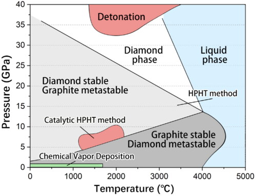
The P-T phase diagram of carbon-diamond is shown in . From the point of view of thermodynamic, at atmospheric pressure and room temperature, graphite is the relatively stable phase of carbon, while diamond is the metastable phase. The phase transformation can be realized only under ultra-high pressure and temperature, where colored by red in the diagram. Fortunately, with the help of catalyst, diamond could be grown via catalytic high temperature and high pressure method to reduce the barrier of temperature and pressure [Citation8], the same as in geological conditions. While detonation is also a well developed and commercialized way for diamond synthetic, but could only produce powder instead of macro-sized crystals.
Figure 1. P-T phase diagram of carbon-diamond.
Static high-pressure high-temperature technique (HPHT) for bulk single crystal diamond (SCD) is quite mature technologies, especially the catalytic HPHT technology, brings about big diamond single crystals [Citation8]. However, even the catalytic HPHT process still needs rather severe conditions of around 1500 °C and 5–6 GPa, which was still difficult to obtain under common manners. But the motivation of making diamond still leads to the development of HPHT device technology. In 1950s, American scientist P.W. Bridgman [Citation9] finally find the way to broke through the threshold condition by designing the special pressure vessel, and the “belt” HPHT devices were successfully achieved by General Electric company according to Bridgman’s idea, which can produce more than 2 GPa pressure and high temperature above 2000 °C, and maintain the needed parameters within the window of diamond growth conditions for more than 1 h. It is regarded as a milestone of a new era of diamond for industrial applications, but it was just the beginning. R&D activities to increase the size, quality and growth rate, to meet the requirement of industry and jewelry market never stopped after that. A chronological is listed below to summarize the development of HPHT diamond technology.
Table 1. Summarization of HPHT technology for large crystal producing.
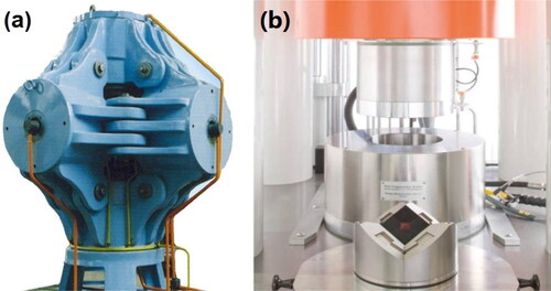
Compared with the belt type presser, a cubic press was designed and mainly used in China since 1963 [Citation13]. Up to now China has hold the biggest production capacity all over the world. Two types of HPHT system mentioned above are shown in .
Figure 2. Cubic type (a) and belt type (b) HPHT systems.
It has been reported that the largest HPHT Diamond belongs to Russia’s New Diamond Technology company [Citation17]. Its largest Diamond rough has even reached 40–60 carats, as shown in , and it is expected to break through 100 carats in following years.
Figure 3. More than 10 ct white and yellow HPHT diamond jewelry by NDT company [Citation17].
![Figure 3. More than 10 ct white and yellow HPHT diamond jewelry by NDT company [Citation17].](/cms/asset/02319c56-b7a1-4522-98cf-63bb1b7c9373/tfdi_a_1869511_f0003_c.jpg)
2.2. Chemical vapor deposition technology
Nevertheless, the HPHT technology still holds its advantages and disadvantages. On the point of engineering view, high temperature and high pressure is not easy to acquire and maintain. Thus, a method which could synthesize diamond under more gentle conditions is demanded. In addition, typical HPHT method requires catalytic, normally metals such as iron, cobalt or nickel, which strongly contaminate the crystal. The last but the most important is, such technique could never achieve thin films and coatings with large area. Although the technology has made breakthroughs and already become the most mature in recent years, there are still technical obstacles to achieve large lateral size with high crystal purity and quality.
Using gas (methane, acetylene, etc.) as raw material, instead of solid carbon is easy to imagine. The earliest report can be traced back to 1962, proposed by Eversole et al. [Citation18]. However, the substrate would be covered by amorphous carbon shortly after the growth starts. Thus only a very thin epitaxial diamond film could be obtained and not able for producing larger crystals. Around 1980s, Spitsyn et al. [Citation19] reported that hydrogen was introduced together with methane, and long termed deposition of diamond film was achieved with the growth rate of 1 μm/h. Angus et al. also discussed the role of hydrogen.
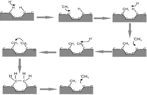
The mechanism of reaction process was briefly shown in . Take methane for example, the reduced mechanism must include following processes: (a) generation of active species and surface radical site. Benefit from the reduction reaction of atomic [H], the substrate surface with H terminal will be activated with generation of dangling bongs, as well as CH* species from gas phase. (b) Attachment of reactive hydrocarbon species to the surface at these sites. Such processes include but not limited to adsorption, diffusion and desorption of the species from the substrate surface. (c) Incorporation of the adsorbate into the diamond lattice, which is the key process of forming new C-C bonds. More detailed mechanisms were described by Goodwin et al. [Citation20].
Figure 4. Principles of CVD diamond process.
As carbon has two kinds of hybridization forms: sp2 and sp3, these two types of bondings will from simultaneously during the deposition, and rapider for sp2 as the bond energy is lower and easier to form. It was found that the presence of atomic hydrogen could inhibit the deposition of sp2 phase by a severe etching. But the etching for sp3 phase is much weaker thus it will retain, which becomes the driving force of continuous deposition of diamond [Citation21]. Since then, chemical vapor deposition (CVD) diamond has really become a possible and valuable method for diamond synthesis, and gradually more advantages of this method have been found, for example highly pure crystal and large area film for optical and electronic applications.
The breakthrough of key technology makes the CVD method develop rapidly. One of the milestones is announcement of the commercialization of polycrystalline diamond products by Element Six was made soon after. In the follow-up developments, methane gas was gradually found to be the best carbon source for diamond growth due to its bonding structure. In addition, the growth equipment and technology on the basis of the earliest heating gas, have evolved into various of kinds such as hot filament method (HFCVD) [Citation22], DC arc plasma jet (DC arc plasma jet) CVD [Citation23], microwave plasma CVD (MPCVD) [Citation24] etc. The most typical equipments, HFCVD and MPCVD, are shown in with schematic drawings, respectively. for other kinds of CVD technique, such as DC arc-jet, RF CVD, etc. were listed and compared.
Figure 5. Photos and schematic of two typical CVD systems, HFCVD and MPCVD.
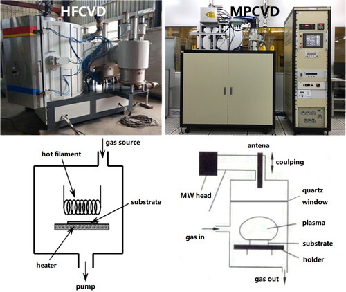
Table 2. Comparison of different CVD techniques.
Among the CVD techniques, microwave plasma assisted CVD methods (MPCVD) was considered as the most advanced and promising for the industrializations. The design of resonator structure brings about a high power density electromagnetic field, generating a highly-active plasma, together with high stability and reliability. In comparison with HFCVD or DC-CVD, microwave as the energy source was introduced by waveguide via quartz window, electrodeless discharge avoids the strong pollution due to the filament sublimation or etching of electrode material. That is why MPCVD method is the only way to produce diamond with very high crystal quality and purity, and controllable doping for electronic and electrochemical applications also becomes reality. Up to now, the earliest and simplest quartz tube deposition equipment has been basically abandoned. According to different coupled mode of microwave by resonant cavity design, different types of CVD systems have been developed, such as “quartz bell jar type” [Citation31], “cylindrical metal resonator type,” “ellipsoid resonator type” [Citation32] and “multi mode cavity” [Citation33] as the main design concept. The high-quality SCD prepared by this technology has been widely used in the fields of optics, electronics and diamond jewelry cultivation. It is also the only diamond mass additive manufacturing technology which can compete with HPHT method.
Unfortunately, the growth of diamond by CVD method still suffers from some bottlenecks. One of them is a limited size of seed crystals of CVD process, normally acquired from natural or HPHT diamond. So the sizes are normally not very large, only within around 3–8 mm. But different from the growth of conventional crystal such as Si and sapphire, the homoepitaxy of SCD is quite special and difficult: subjected to the phase transformation under high temperature, diamond can not grow in the melting-recrystallization mode like traditional crystal, which can only be realized by polar environmental phase change (HPHT), or deposition from vapor phases. What’s worse, the “edge effect” caused by plasma overconcentrating at the border of substrates results in severe polycrystallization around the crystal during the growth, which strongly reduces the area of single crystal, thus limits the increase of usable SCD area. That’s why synthetic diamond still hard to break through the restrict of small size, and only can meet the requiring size of jewelry market, but still far away from the inch size demands for advanced optical, thermal and electrical industrial applications. In addition, dislocation accumulation and even twinning in the growth process restrict the quality of epitaxial diamond layer. High quality and high growth rate are difficult to obtain simultaneously for effective production. Problems above are the core scientific issues in the homoepitaxial growth of diamond single crystal. It is also a technical obstacle to the wider industrial application of diamond.
3. Coessential-connection growth of diamond
The concept of “Coessential connection” is not new in material science, especially welding technology. Traditional fusion welding and brazing technology can be regarded as the category of coessential-connection.
However, diamond materials are very different from the typical metal materials: although the theoretical melting point of diamond is about 3500–4000 °C, in fact, from the carbon P-T phase diagram in , we know that diamond is a thermodynamic metastable phase under relatively low temperature and pressure range, while graphite is stable. Therefore, if the diamond is simply heated up without sufficient pressure, even in vacuum the phase transformation of diamond will occur, atomic structure will be changed into graphite and irreversible. Just because of such special physicochemical properties of diamond material, the connecting process is completely different from that of classical welding technology by melting the matrix or brazing filler metal. Therefore, diamond can not be bonded by traditional technology. However as discussed above, to increase the size of diamond is critically needed for the practical use, thus the new approach to connect diamond and to acquire large size or special structure is highly demanded and very challenging.
3.1. “Mosaic” growth of SCD
A simple but effective way to solve the problem of undersized substrate is the so called “mosaic” growth. The general idea is obvious: if one piece of substrate is limited by the small size, and the growth mechanism also restricts the lateral expansion, then put together crystallographically aligned several pieces with same dimensions in close proximity.
For diamond mosaic growth, the process is schematically shown in . The substrates are shown by yellow and the epitaxial layer is in white color in order to distinguish. Note that the substrates could be either HPHT, or CVD and even natural diamonds, but should be single crystalline diamond slices, generally within several mm lateral size and less than 1 mm thick. Large surface normally was laser cut and precisely polished, with (100) orientation which regarded as the best facet for diamond epitaxial growth due to lower defect formation than for other orientations. Several pieces are tightly arranged on a substrate holder, and diamond deposition takes place simultaneously on each piece. The extending elements of the picture finally joint with each other integrating into one big piece of free standing layer.
Figure 6. Schematic of diamond “mosaic” growth process [Citation34].
![Figure 6. Schematic of diamond “mosaic” growth process [Citation34].](/cms/asset/8f47c3f3-75a3-4e0c-a388-2698cf204630/tfdi_a_1869511_f0006_c.jpg)
The first attempt to realize the mosaic growth was done by Geis et al. [Citation35], who used a Si substrate with regular pyramid pits array as the template, seed it with similarly oriented diamond particles, and obtained ∼240 μm thick mosaic diamond layer after 80 h deposition. Although the overgrown layer was not perfect, with holes because of the miss seeding of some pits, yet it showed a way to break through the limitation of very small substrate as the first attempt. The same group tried again such idea with slightly larger cubic seeds with (100) facets, a joint film was prepared but due to the small size and irregular arrangement of the substrates, it still far from designed single crystal structure [Citation36]. The real mosaic SCD was prepared by Janssen et al. [Citation34]. They used SCD seed substrates with reduced misorientation was studied, and produced a joint mosaic diamond plate with significantly increased surface. At the next step, two, four and even seven pieces of grown mosaics were used by them for further enlargement of the mosaic diamond area. This so called “two step” process was tried, with short-tome HFCVD diamond deposition for bridging the gaps between the substrates, followed by high-rate growth using oxygen combustion flame method to deposit a thicker film (∼250 μm) [Citation37]. Schermer et al. [Citation38] studied carefully the surface morphology and the structure of joint part, the junction between elements of mosaics by SEM and Raman spectroscopy. In the same year, Posthill et al. [Citation39, Citation40] also successfully prepared mosaic diamond by the similar approach, but using Ni coating to bond the substrates in one body and performing epitaxial growth by RFCVD. Findeling-Dufour et al. [Citation41, Citation42] characterized the quality of diamond substrate and mosaic junctions in detail. The effects of misorientation angle and quality of diamond seeds on the growth mode were studied in splicing experiments for different substrates. Kobashi et al. [Citation43] produced a 12 mm size mosaic diamond from 16 pieces of SCD seeds using a 915 MHz MPCVD system.
Further progress was reported only after the year of 2008, by Y. Mokuno and H. Yamada group from AIST, Japan [Citation44, Citation45], who developed the so called “lift-off” method. High energy C ion implantation from hundreds of keV to several MeV in diamond substrates was performed before the CVD process to create a highly defective sub-surface layer at depth of several micrometers beneath the surface. The damaged layer was converted into graphite during the diamond deposition or afterwards heat treatment, and the grown CVD diamond film was detached by etching of the buried graphite in acid. The “clone” substrates with rather similar and controllable parameters of size, orientation and thickness, were produced by this repeated “lift-off” process as the seeds for further mosaic growth in order to improve the quality of mosaic junctions. The process is schematically shown in . One inch mosaic diamond was produced by this approach [Citation46–50], and later a mosaic plate with 40 × 60 mm2 was demonstrated successfully made, which remains to be one of the largest mosaic diamond single crystal [Citation51]. The representative samples are also displayed in .
Figure 7. Schematics of “Lift-off” technology for clone substrates production (top picture), and the 1–2 inch mosaic samples (bottom images) [Citation49–51].
![Figure 7. Schematics of “Lift-off” technology for clone substrates production (top picture), and the 1–2 inch mosaic samples (bottom images) [Citation49–51].](/cms/asset/468dd0cb-63c3-418c-ae7d-0f76d912a842/tfdi_a_1869511_f0007_c.jpg)
As a further increase of the mosaic’s size met problems of maintaining radial uniformity, attention has been turned to characterization and optimization of mosaic junction structure. Ohmagari et al. [Citation52] investigated electrical properties effected by the defects in the junction region, especially dislocations. A large leakage current with an inferior Schottky barrier height has been observed at the boundary, and a buffer layer was introduced to mitigate the dislocation density aggregated on coalescence junctions and to further improve the device uniformity. Tallaire et al. [Citation53] prepared the mosaic diamond with 7 pieces, with the observation of polycrystallined junction with a strong fluorescence of blue light under UV emission, indicating the presence of stress and cracks at the interconnection. Raman spectrum scans crossing the junction revealed a broadening of the diamond peak and shift of its position that indicated a deterioration of the crystal structure around the junction [Citation54–56]. Muchnikov et al. [Citation54] studied a mosaic diamond plate with four interfaces, with comprehensive measurements using Raman mapping for stress and defect distributions, X-ray diffraction and rocking curve for orientations, and secondary ion mass spectrometry (SIMS) for impurity content evaluation. Wang et al. [Citation55] carried out a similar research, with more attention to surface morphology on the substrates and within junction. Shu et al. [Citation56] used Raman mapping on cross section of mosaic junction, from substrate to the top surface to trace the evolution of defective zone adjacent to the junction along with the deposition. A tendency was found that the width of stress affected and defect enriched region around the junction extending from bottom to top with the film thickness, from ∼40 μm wide on the film-substrate interface to about 250 μm in top layer above the substrate. Based on the experience with optimal growth conditions, the diamond mosaics with 1 inch length, and 2 inch in diameter, has been produced at Harbin Institute of Technology ().
Figure 8. 1 and 2 inch mosaic diamond sample prepared by HIT group
3.2. Epitaxial lateral overgrowth
The epitaxial lateral overgrowth (ELO) is still not wide spread process for diamond synthesis, but a traditional method for the growth of crystal, SiO2 and GaN for instance, especially by the CVD technique [Citation57, Citation58]. Recent years the ELO has been introduced in homoepitaxial diamond growth technology [Citation59–61], aimed at forming a buried metal pattern as electrodes, or a mask to stop the growth of threading dislocation and improve the size and quality of the epitaxial layer. Bauer et al. [Citation62] deposited thin Ir layer with a mesh of 10–200 nm holes on SCD substrates, with further diamond growth though the Ir mask to form a complete overgrowth layer and characterized its properties by XRD and Raman spectroscopy. Wang group [Citation63] used a similar method to mask the diamond with Ir strips to block the epitaxy under the Ir and form the overgrowth layer by ELO (). The improvement of the ELO film was confirmed by a decrease of the number of dislocation related etch pits compared to conventionally grown material. A UV photodetector device was constructed based on such structure. They also fabricated microfluidic channels via strip masks along with ICP etching technology to fabricate groves (width of 2.35 μm and height of ∼20 μm) on the diamond substrates [Citation64] as illustrated in .
Figure 9. Epitaxial lateral overgrowth (ELO) of CVD diamond [Citation63, Citation64].
![Figure 9. Epitaxial lateral overgrowth (ELO) of CVD diamond [Citation63, Citation64].](/cms/asset/4c7ea2df-0b76-4d6e-890e-4de42b5ac3fa/tfdi_a_1869511_f0009_c.jpg)
Tallaire et al. [Citation65] realized an interesting idea of ELO on a special SCD substrate with a major central part removed. The standard HPHT substrate was laser cut to create a square-shape through hole in the center, and subjected to etch treatment to remove the laser-induced graphitized surface layer (). Then, diamond deposition was carried out using their optimized condition. A ∼1 mm thick CVD layer was acquired, with the completely fused central part owing to the lateral growth. The hole disappeared, leaving a top surface consist of smooth center and surrounding uniform growth steps, free of any unepitaxial defects. Cathodoluminescence images and etching treatment were employed to show that the dislocation density is much reduced in the material above the hole. The mechanism of the effect was proposed based on idea that the threading dislocations will extend vertically along with the growth direction, or within some growth sectors of (110) or (111) faces, but only very few will stretch into the ELO part which grown perpendicular to the direction of original dislocations, and the optimized condition also limited the generation of new defects. The concept is illustrated in more detail in .
Figure 10. ELO of SCD by hollowing out the central part of substrate and thus suppress the extension of dislocation [Citation65].
![Figure 10. ELO of SCD by hollowing out the central part of substrate and thus suppress the extension of dislocation [Citation65].](/cms/asset/41ce4cf0-f968-4104-b4c9-d92cd68b1e3a/tfdi_a_1869511_f0010_c.jpg)
Aida et al. [Citation66, Citation67] developed an original version of ELO with diamond micro needles with high aspect ratio fabricated on a HPHT substrate using deposition of Ni mask followed by thermo-chemical etching, with subsequent diamond growth process to join the needles into continuous diamond homoepitaxial layer, while keeping air gaps between the needles. The weak mechanical link of the substrate and the epilayer facilitates easy separation of the top plate from the substrate, and prevents the bulk diamond layer from cracking. The ELO on the needle tips also leads to a promotion of epilayer quality by means of reduction of the defect evolution.
3.3. Heteroepitaxial growth of diamond on Ir and patterned growth
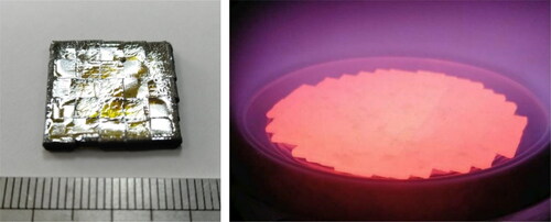
Heteroepitaxial growth on a non-diamond material is alternative to homoepitaxy to produce CVD SCD. The key point of heteroepitaxy is to satisfy two principal demands, namely to design and prepare a proper multilayer film substrate with a good match to diamond lattice, and the controlled nucleation process. After decade of exploration, the optimal substrate has been found to be the single crystalline Ir [Citation68]. While a bias enhanced nucleation (BEN) method by applying a negative DC voltage on substrate, is considered as the most useful diamond nucleation (formation of seeds) technique. Many studies have been performed trying to improve the nucleation and growth regimes [Citation69–72], and finally at the year of 2017, Schreck et al. [Citation73] from Augsburg University produced the largest CVD SCD of 92 mm in diameter and 155 carat weight, till now still the keeper of world record, shown in .
Figure 11. Largest single crystal CVD diamond by heteroepitaxial growth [Citation73].
![Figure 11. Largest single crystal CVD diamond by heteroepitaxial growth [Citation73].](/cms/asset/3800d91e-dddc-4c6b-8a64-4752aba688b3/tfdi_a_1869511_f0011_c.jpg)
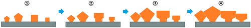
However, the due to the mismatch of Ir and diamond lattice (∼7.1%), mosaicity between nuclei, as well as the relatively poor quality of Ir substrate, the quality of all epitaxial diamond remain low, rich in defects and stress, and its quality still did not reach that for best homoepitaxial films. Nevertheless, substantial improvements have been achieved in recent years, particularly, it was demonstrated that the charge carriers mobility could be comparable with the parameters known for electronic grade CVD diamond [Citation74]. Patterned growth, a version of ELO approach, was developed by Sawabe et al. [Citation75–80] to improve the structure of epilayer on Ir substrates. They used a patterned resist mask to save the nucleation sites in selected areas, while etched away unmasked part under the treatment by a neutralized Ar beam. Afterwards the substrate was submitted to diamond growth process. The unmasked area is not involved in the diamond growth as the nuclei were destroyed during the etching. The patterns with nuclei integrated into one larger nucleus, normally with pyramid shape consist of four (111) face due to the relative deposition rate of different orientations under controlled parameters. The patterned nuclei continue to enlarge horizontally, joint with neighbors, and eventually form a continuous film as shown in . Other shapes of patterns such as strips are also studied, and the dislocation density were compared and proved to be effective for upgrade the CVD layer quality. The process of pattern evolution via lateral growth and joint are displayed in .
Figure 12. Evolution of Patterned nucleation growth based on diamond heteroepitaxy [Citation80].
![Figure 12. Evolution of Patterned nucleation growth based on diamond heteroepitaxy [Citation80].](/cms/asset/b3ec9c88-135b-4de8-bfaf-ade44cfe88a1/tfdi_a_1869511_f0012_b.jpg)
The patterned nucleation growth method described above is just an expressive example of lateral growth to control epitaxy. In fact, any heteroepitaxial growth of diamond is based on the same principle, as explained in next section.
3.4. Generalized idea of coessential-connection growth
In a broad sense, the coessential-connection process of diamond is actually one of the earliest and most widely used processes of CVD synthetic diamond films. However, this concept has not been clearly proposed. The notion of “mosaic growth,” as the narrow sense, proposed by Geis and Jansson in the early 1990s is still used to connect SCD. But in fact, the concepts of “mosaic” and “homogeneous connection” are not exactly the same: the so-called “mosaic” is mainly concerned with the arrangement and composition of a geometric shape, composed by pieces of similar size and arranged into patterns with certain orders. Thus “mosaic growth” method emphasizes the placement of the seed crystals.
In fact, the process of epitaxy, expansion and interconnection to form a whole is the core of mosaic growth, from the point of view of crystal growth dynamics. If there is no transverse expansion and joint closure during the growth process, the simple mosaic arrangement will always be independent and scattered diamond pieces, which can never aggregate and obtain the large area self-standing SCD film. This is also the reason that in some applications like device, such as CERN’s SCD high-energy particle detection array, even if there is no material growth process, it can be called “mosaic” detector, shown in [Citation81].
Figure 13. Diamond mosaic detector by CERN [Citation81].
![Figure 13. Diamond mosaic detector by CERN [Citation81].](/cms/asset/c52f6209-0aa8-4054-acd3-00e0c1cd5edf/tfdi_a_1869511_f0013_c.jpg)
Therefore, “coessential-connection” (CC) growth technology is more suitable word for stating the concept of the diamond deposition process for achieving large area SCD layer by CVD method. The real core of this concept is not limited to mosaic growth, but can be extended to a broader and macroscopic point of view: in single crystal epitaxy, polycrystalline diamond film formation and heteroepitaxial SCD, such processes above also hold the same intrinsic essence, as shown in .
Figure 14. Schematic of nucleus growth and connection dynamic in coessential-connection
3.4.1. Isolated initial diamond “nucleus”
The broad sense of “diamond nucleation” is not only limited to the traditional nucleation for poly/nanocrystalline diamond, but also includes the following types: (a) isolated island growth mode (Volmer-Weber mode) for homoepitaxy of single crystal, (b) various micro-nano structures (patterned growth) followed by ELO, (c) nucleation seeded and secondary nucleation during poly/nanocrystalline growth, (d) nucleation without seeding process such as bias-enhanced nucleation in heteroepitaxial growth, and (e) artificially arranged diamond plates, namely mosaic growth. The origin of nucleus is regardless, whether artificially or by physical/chemical process, and also the size as well. In most cases above, the nuclei will have the same essential properties, that is, they are independent respectively, and not form a whole (including those with too close position and touched with each other, but not aggregated). For homoepitaxy, heteroepitaxy and mosaic growth, the “nuclei” are typically monocrystalline, and within approximately the same orientations or small mosaicity. For polycrystalline and nanocrystalline, the nuclei could be either single crystalline or poly, even amorphous, with random orientations. As shown in , orange color represents the crystal nucleus, and different forms and shapes are adopted to illustrate possible multiple orientations and morphologies.
3.4.2. The growth of diamond nuclei
When the nucleus is already exist and in a suitable carbon containing growth environment (plasma or hot gas), hydrocarbon radicals react with the surface to attach new carbon atom to diamond lattice [Citation82], while the crystal growth take place, based on the original structure of nuclei. Specific growth process and morphology evolution is defined by plasma conditions according to the relative deposition rate of different planes [Citation83]. But in any case, the scale enlargement in all directions is inevitable for free surfaces, that is, when artificial geometrical restrictions (masks, templates) are absent. In another word, the crystal nuclei will grow in vertical and lateral direction simultaneously.
3.4.3. Contact of diamond nuclei
Although the position and distance of diamond nuclei could be different under different conditions, ranging from nano scale (high density nucleation process of nanodiamond) to even centimeter scale (such as mosaic growth), the original distance between nuclei will gradually decrease because of lateral enlargement of each crystal nucleus during CVD process. The gaps between nuclei will eventually shrink to zero, as the contact occurs. The atomic level of the primary contact at certain time, the stable formation of chemical bonds between one particular carbon atom with two independent nuclei together (that atom closes the atomic scale gap between the neighbor crystals). The origin of the bridging carbon atom could be either from plasma, or due to surface diffusion from other zone, it should remain as a stable atom without desorption or etched away. We call such atoms the “primary connecting atoms” as a symbol of the CC growth process. The occurrence of the above process can be regarded as the formation of zero dimensional contact interface, and will evolve further into larger dimensions.
The “primary connection” is only an instant event, while deposition is sustaining. The interface between nuclei gradually develops at the junction. After contact bonding, the lateral growth beneath the connected part stopped, due to the plasma could not penetrate, and leave an unconnected space. Such case commonly happens in mosaic growth [Citation56].
3.4.4. Vertical extension and evolution of interface
The existence of the interface leads to the destruction of the lattice structure of carbon atoms to a certain extent, which leads to the accumulation and expansion of defects and stresses, and even the appearance of twins (or secondary nucleation), which will affect the surrounding region. Different bonding interfaces have different states, such as competitive growth of polycrystalline grains, the expansion and evolution of interface influence zone in mosaic splicing process, and the interaction of small angle grain boundaries in heteroepitaxial growth. Since there are many cases, the process is not shown. However, in any case, the existence of the interface is unavoidable, and often has a relatively negative impact on the crystal quality. Therefore, the optimization and relative control become the key problems in related work [Citation84].
In summary, the coessential-connection growth is not only a narrow for mosaic growth, but also appropriate for heteroepitaxy, and even poly/nanocrystalline diamond growth. In the photo and schematic shows the cross section of a polycrystalline diamond film, where the columnar crystals are clearly seen [Citation85, Citation86]. The lateral growth and joint also happened to poly and nano crystalline film, which is contained in the framework of CC growth [Citation87]. Moreover, we found that such phenomenon also happened during the first stage of simple homoepitaxial diamond growth [Citation88]. The step morphology will be disturbed by the interruption of deposition. New isolated particles form shortly after the successive growth, and connect with each other to restore the growth steps by bunching process [Citation89].
Figure 15. SEM and schematic of polycrystalline diamond cross-section [Citation86].
![Figure 15. SEM and schematic of polycrystalline diamond cross-section [Citation86].](/cms/asset/be0f5840-0270-4cba-af8a-5ba8bce301d6/tfdi_a_1869511_f0015_b.jpg)
3.5. Interface formation and mechanism
The essence of the interface formation is a dynamic process of the closure of the original independent nuclei, in another word, the disappearance of the original surface of the nuclei and the formation of the new interface between the nuclei. The thermodynamic expression can be described by the following formula: where ΔG is the Gibbs free energy change of the system, Na, Nb, Nab are the atomic numbers of nuclei a, B and AB, respectively, and μa, μb, μab are the Gibbs free energy per atomic unit of the corresponding nuclei.
are the surface energy of nuclei a, b and combined nuclei ab, respectively.
is the interface energy for the formation of a new interface between nuclei. Since the nucleation is a spontaneous process in growth, the interfacial energy
should be lower than the differential of surface energy between isolated and combined, and the total free energy of the system will decreases.
Should note that, perfect crystal doesn’t exist in reality, and the same as perfect interface. No matter how serious the adjustment was made to arrange the nuclei, there must be a deviation of crystal size and orientation between each other. Not to mention in most cases, the nucleation of seed crystals are randomly arranged and the size are too tiny to be controlled. Therefore, disclinations and grain boundaries do formed at the junction, which is the most common interface between diamond nucleus. In addition, the interface will also be affected by stacking fault or extension of initial dislocation, which are unavoidable in the transverse growth, resulting in the formation of neonatal defects. Thus the possibility of complete connection with exactly the same orientation at atomic level is rather low and negligible.
No matter macroscale CC growth like mosaic, or nanosized nuclei like the nucleation of heteroepitaxial growth, the mismatch of size and orientation are inevitable. For difference of nucleus sizes, especially the thickness which impact more serious, difference of seeds can be a few times, or as large as hundreds of microns. Therefore, nuclei with different height may stay in different environment with a significant deviation of plasma concentration or temperature, which result in a quite different growth rate and morphology evolution. The larger and higher nucleus normally will gain even faster growth, and further augment the difference by positive feedback, while the small nucleus could be even slower and smaller by contrast. So the larger seed could even “swallow” the smaller seed crystal in serious cases ().
Figure 16. Deviation of (a) nuclei size and (b) orientations.
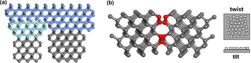
What’s more, surface misorientation from the standard crystal plane caused by the machining, irregularly formation process or simply placement, it is almost impossible to control the orientation of diamond nuclei to be completely consistent. As shown in , the orientation deviation is shown obviously shown by a mode, which can be divided into three categories: (a) out of plane orientation deviation in omega direction (Y-Z plane) or phi direction (x-z plane), namely “tilt,” and (b) in-plane psi direction (X-Y plane), the “twist”; and (c) both in-and-out of plane deviation exist, a mixture of tilt and twist. X-ray diffraction and rocking curve measurement are often adopted for the characterization of mosaicity mentioned above. The existence of any deviation will lead to the formation of small angle grain boundary. In , the interface atoms which constitute the small angle grain boundary are marked with red color. Some of the cases during the growth of heteroepitaxial nuclei, a small enough deviation of orientation could be close by transformation into disclination and even diminish, due to the gathering, mutual reaction, overgrowth and stress induced occlusion [Citation90]. While if the misorientation was larger than 1°, such case above will not happen and the material will not be considered as single crystal.
3.6. Comparison of different typed CC growth
CC growth as mentioned above, embracing the CVD diamond growth based on similar procedures but with various of nuclei states. Here we summarize and classify the states from different aspects as following.
3.6.1. Size of wafer and the trend
The core objective of CC growth is to prepare wafer scale diamond film with high quality, for the advanced applications of electronics, optics and thermal managements. Here the latest progress of large size diamond film, with different approaches have been summarized, as listed in .
Table 3. Summarization of large area diamond film.
Obviously, although huge PCD diamond films were able to be prepared even 20 years ago, the breakthrough of large area SCD wafer, are only achieved in recent 3–5 years, benefit by not only the CC growth technique including mosaic growth and heteroepitaxial growth, but also the development of MPCVD system. Longer wavelength (normally 915 MHz, commonly used industrial microwave frequency), or gyrotron sources for 28–30 GHz [Citation93], together with higher power and larger cavity, will generate big plasma covering enough area, approximately 4–6 inch, with preferable uniformity, enabling the deposition of diamond film. Design and manufacture of new type MPCVD system seems to be also an important task in this field.
3.6.2. Grain size and mosaicity
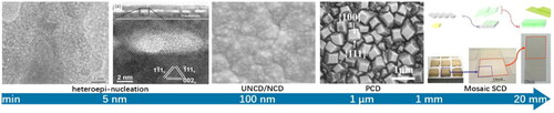
Interface formation influenced by the difference of nuclei sizes have been discussed in previous. While, for different types of CC growth, such as PCD and SCD, the size of nucleuses of different kinds of diamond film could various from nano to macro. The smallest diamond particle could be about 2–5 nm, containing SiV color centers [Citation94]. While for typical PCD and NCD film, nucleation size could be as large as hundreds or nanometer to micrometers, depend on the processing of substrate and growth condition. The other extreme is obviously the mosaic growth, the macro-sized nuclei, or substrate in another word, a few millimeters or even up to 40 mm by Yamada et al. [Citation51]. A summarization of grain size from nano scale to macro has been listed in .
Figure 17. Grain size from smallest to largest within the framework of CC growth.
The surface reaction and nucleation is defined by the surface energy of substrate γs, interface energy γi and deposition energy γd. The energy change, namely nucleation energy ΔG, as the driving force of such process. Thermodynamic conditions need to be satisfied as γd + γi > γs, to achieve the isolated nucleation instead of two dimensional spreading.
The minimum size of nucleation could be defined by following equationwhere r is the radius of nucleus, v is the volume of single atom or molecule, Δg is the unit Gibbs free energy change by single atom/molecule, γsn is the unit surface energy of formed nucleus, γss is the unit surface energy of substrate. As diamond nucleation by CVD process is on diamond or heterogeneous substrate such as Si and Ir, the dimension of nucleus could various within several nanometers or less. The smallest nucleus reported by Lifshitz et al. [Citation95] on Science was found to be 3 nm, while in the work of Schreck et al. [Citation96] is about 10 nm, and the size of domain by CC growth at the primary state can be as large as 257 nm.
For NCD and PCD diamond, the size of nuclei strongly depend on the seeding process, including the original size of seeds, method of seeding (ultrasonic, spin or scratch, etc.). In addition the secondary nucleation could be regarded as obeying the rules of thermodynamic described above. Mosaic diamond could be considered as a kind of seeding process with macro-sized seeds, several mm or even tens of mm. As the size is large enough to manipulate, the orientation become controllable, while NCD/PCD is definitely randomly orientated. In comparison, mosaic diamond definitely hold the highest crystal quality, even where the junction locates exceeds the normal heteroepitaxy, let along NCD/PCD. Nevertheless, mosaic diamond can hardly increase further the entire area, size of single piece SCD substrate still is the strongest limitation, as well as the exorbitant cost and enhance of proportion of junction area. Heteroepitaxy, although restricted by the quality of substrate films and unmanageable growth technology, it necessarily be the indispensable way for preparation of ultra-large SCD wafer.
4. Conclusion
A concept of “Coessential connection” growth of SCD is summarized, based on the research of CVD diamond preparation technology. The CC growth process is a common way to break through the bottleneck of substrate size limitation, and to produce a large size diamond freestanding film with high crystal quality and multi-structures. Typical results such as mosaic growth and patterned growth of heteroepitaxial were listed as the representative results for 2–4 inch SCD diamond. While ELO process was also discussed for dislocation restraining and quality improving. The CVD technique above could be included in CC growth idea, which could be considered as a universal concept throughout the field of CVD diamond film growth and preparation. Nucleation mechanism, size and the film size can be reached with different approaches of CC growth were compared and summarized, together with the prospect of the trend of future.
Disclosure statement
No potential conflict of interest was reported by the authors.
Funding
This work was supported by National Natural Science Foundation of China (Grants Nos. 52072087, 51702066), National Science Fund for Distinguished Young Scholars (Grant No. 51625201), National Key Research and Development Program of China (Grant No. 2016YFE0201600), 1000 Talents Program, and China Scholarships Council.
Additional information
Notes on contributors
Guoyang Shu
Dr. Guoyang Shu graduated from Harbin Institute of Technology and studied also in General Physics Institute RAS. He’s major in the growth and characterization of high-quality, large-size single crystal diamond, especially diamond mosaics, as well as nanostructured diamond preparations.
Dr. Bing Dai works in Harbin Institute of Technology now. The main research interests include diamond materials and new carbon materials.
Dr. Andrey Bolshakov, senior researcher from General Physics Institute of Russian Academic of Science, focused on the high rate growth of high-quility diamond material as well as plasma diagnosis.
Mr. Weihua Wang, PhD student from Harbin Institute of Technology. Devote himself to the preparation technology of hetroepitaxial diamond and design of substrates.
Ms. Yang Wang, studying in Harbin Institute of Technology as a PhD candidate. Her current research topic is about simulation of nucleation process, substrate and films-interface performance for diamond heteroepitaxy.
Dr. Kang Liu is a postdoctoral researcher in Harbin Institute of Technology, majoring in the physical properties and new phenomenons of diamond wide bandgap semiconductor material and its optoelectronic applications.
Mr. Jiwen Zhao obtained bachelor’s degree in Harbin Institute of Technology, and continuing to complete his doctorate degree. His major research interest is the diamond growth and applications in thermotics.
Prof. Jiecai Han is an academician of Chinese Academy of Science and the vice president of Harbin Institute of Technology. The main research interests include synthesis and characterization of advanced and functional materials including composites, crystals and photoelectronic thin film technologies.
Prof. Jiaqi Zhu is a PhD supervisor, Cheung Kong Scholars Chair Professor, Outstanding Young Investigator Award, Leading Talent of “the Ten Thousand Talents Program”. The main research interests include functional photoelectric crystals and films.
References
- Fang J, He Z, Zhang Z, et al. Reliability improvement of diamond drill bits using design of experiments. Qual Eng. 2018; 30(2): 339–350.
- Wang XC, Shen B, Sun FH, et al. Deposition and application of CVD diamond films on the interior-hole surface of silicon carbide compacting dies. KEM. 2012; 499: 45–50.
- Jayaraman A. Diamond anvil cell and high-pressure physical investigations. Rev Mod Phys. 1983; 55(1): 65–108.
- Inyushkin AV, Taldenkov AN, Ralchenko VG, et al. Thermal conductivity of high purity synthetic single crystal diamonds. Phys Rev B. 2018; 97(14): 144305.
- Graebner JE, Reiss ME, Seibles L, et al. Phonon scattering in chemical-vapor-deposited diamond. Phys Rev B. 1994; 50(6): 3702–3713.
- Simon RB, Anaya J, Faili F, et al. Effect of grain size of polycrystalline diamond on its heat spreading properties. Appl Phys Express. 2016; 9(6): 061302.
- Rossini FD, Jessup RS. Heat and free energy of formation of carbon dioxide, and of the transition between graphite and diamond. J Res Natl Bur Stan. 1938; 21(4): 491–513.
- Palyanov YN, Kupriyanov IN, Khokhryakov AF, et al. Crystal growth of diamond. In: Handbook of crystal growth: bulk crystal growth. 2nd ed. New York (NY): Elsevier; 2015. p. 671–713.
- Bundy FP, Hall HT, Strong HM, et al. Man-made diamonds. Nature. 1955; 176(4471): 51–55.
- Bovenkerk HP, Bundy FP, Strong HM, et al. Preparation of diamond. Nature. 1959; 184(4693): 1094–1098.
- Strong HM, Wentorf RH. The growth of large diamond crystals. Die Naturwissenschaften. 1972; 59(1): 1–7.
- Sumiya H, Satoh S, Nishibayashi Y. Development of high-purity synthetic diamonds. Sumitomo Electr Tech Rev. 1995; 39: 69–69.
- Wang G. The birth of China’s first synthetic diamond (in Chinese). Superhard Mater Eng. 2008; 4: 45–47.
- Shigley J, Moses T, Reinitz I, et al. Gemological properties of near-colorless synthetic diamonds. Gems Gemol. 2010; 46: 42–53.
- Hainschwang T, Simic D, Fritsch E, et al. A gemological study of a collection of chameleon diamonds. Gems Gemol. 2005; 41(1): 20–35.
- D’Haenens-Johansson UFS, Moe KS, Johnson P, et al. Near-colorless HPHT synthetic diamonds from AOTC Group. Gems Gemol. 2014; 50: 30–45.
- D’Haenans-Johansson UFS, Katrusha A, Moe KS, et al. Large colorless HPHT-grown synthetic gem diamonds from New Diamond Technology, Russia. G&G. 2015; 51(3): 260–279.
- Eversole WG. Synthesis of diamond. US Patent No. 3,030,188. 1962.
- Spitsyn B. v, Bouilov LL, Derjaguin B. Vapor growth of diamond on diamond and other surfaces. J Cryst Growth. 1981; 52: 219–226.
- Goodwin DG. Scaling laws for diamond chemical-vapor deposition. I. Diamond surface chemistry. J Appl Phys. 1993; 74(11): 6888–6894.
- Wang JT, Huang ZQ, Wan YZ, et al. Thermodynamic coupling effect and catalyst effect for the artificial diamond growth. J Mater Res. 1997; 12(6): 1530–1535.
- Wang H, Shen X, Wang X, et al. Simulation and experimental researches on the substrate temperature distribution of the large-capacity HFCVD setup for mass-production of diamond coated milling tools. Diamond Relat Mater. 2020; 101(107610): 107610.
- Smith JA, Rosser KN, Yagi H, et al. Diamond deposition in a DC-arc jet CVD system: Investigations of the effects of nitrogen addition. Diamond Relat Mater. 2001; 10(3–7): 370–375.
- Mallik A, Microwave plasma CVD grown single crystal diamonds – a review. J Coat Sci Technol. 2016; 3(2): 75–99.
- Matsumoto S, Sato Y, Tsutsumi M, et al. Growth of diamond particles from methane-hydrogen gas. J Mater Sci. 1982; 17(11): 3106–3112.
- Kamo M, Sato Y, Matsumoto S, et al. Diamond synthesis from gas phase in microwave plasma. J Cryst Growth. 1983; 62(3): 642–644.
- Matsumoto S. Chemical vapour deposition of diamond in RF glow discharge. J Mater Sci Lett. 1985; 4(5): 600–602.
- Kurihara K, Sasaki K, Kawarada M, et al. High rate synthesis of diamond by dc plasma jet chemical vapor deposition. Appl Phys Lett. 1988; 52(6): 437–438.
- Hanssen LM, Carrington WA, Butler JE, et al. Diamond synthesis using an oxygen-acetylene torch. Mater Lett. 1988; 7(7–8): 289–292.
- Hiraki A, Kawarada H, Wei J, et al. Preparation and characterization of wide area, high quality diamond film using magnetoactive plasma chemical vapour deposition. Surf Coat Technol. 1990; 43–44: 10–21.
- Hassouni K, Silva F, Gicquel A. Modelling of diamond deposition microwave cavity generated plasmas. J Phys D: Appl Phys. 2010; 43(15): 153001.
- Füner M, Wild C, Koidl P. Novel microwave plasma reactor for diamond synthesis. Appl Phys Lett. 1998; 72(10): 1149–1151.
- Bolshakov AP, Ralchenko VG, Yurov VY, et al. High-rate growth of single crystal diamond in microwave plasma in CH4/H2 and CH4/H2/Ar gas mixtures in presence of intensive soot formation. Diamond Relat Mater. 2016; 62: 49–57.
- Janssen G, Giling LJ. “Mosaic” growth of diamond. Diamond Relat Mater. 1995; 4(7): 1025–1031.
- Geis MW, Smith HI, Argoitia A, et al. Large-area mosaic diamond films approaching single-crystal quality. Appl Phys Lett. 1991; 58(22): 2485–2487.
- Geis MW, Efremow NN, Susalka R, et al. Mosaic diamond substrates approaching single-crystal quality using cube-shaped diamond seeds. Diamond Relat Mater. 1994; 4(1): 76–82.
- Janssen G, Schermer JJ, Giling LJ. Towards large area diamond substrates: the mosaic process. Proceeding of Materials Research Society Symposium. 1996. vol. 416, p. 33–44.
- Schermer JJ, de Theije FK, Giling LJ. Mosaic growth of diamond: a study of homoepitaxial flame deposition and etching of {001}-oriented diamond layers. J Cryst Growth. 1996; 165(4): 387–401.
- Posthill JB, Malta DP, Humphreys TP, et al. Method of fabricating a free‐standing diamond single crystal using growth from the vapor phase. J Appl Phys. 1996; 79(5): 2722–2727.
- Posthill JB, Malta DP, Hudson GC, et al. Demonstration of a method to fabricate a large-area diamond single crystal. Thin Solid Films. 1995; 271(1–2): 39–49.
- Findeling-Dufour C, Gicquel A. Study for fabricating large area diamond single-crystal layers. Thin Solid Films. 1997; 308–309: 178–185.
- Findeling-Dufour C, Gicquel A, Chiron R. Growth of large single-crystal diamond layers: analysis of the junctions between adjacent diamonds. Diamond Relat Mater. 1998; 7(7): 986–998.
- Kobashi K, Nishibayashi Y, Yokota Y, et al. R&D of diamond films in the Frontier Carbon Technology Project and related topics. Diamond Relat Mater. 2003; 12: 233–240.
- Mokuno Y, Chayahara A, Yamada H. Synthesis of large single crystal diamond plates by high rate homoepitaxial growth using microwave plasma CVD and lift-off process. Diamond Relat Mater. 2008; 17(4–5): 415–418.
- Mokuno Y, Chayahara A, Yamada H, et al. Large single crystal diamond plates produced by microwave plasma CVD. MSF. 2009; 615–617: 991–994.
- Yamada H, Chayahara A, Mokuno Y, et al. Fabrication of 1 inch mosaic crystal diamond wafers. Appl Phys Express. 2010; 3(5): 051301.
- Yamada H, Chayahara A, Mokuno Y, et al. Recent progresses in R&D of methods to fabricate inch-sized diamond wafers. In: Materials Challenges and Testing for Manufacturing, Mobility, Biomedical Applications and Climate. Cham (Switzerland): Springer; 2014. p. 97–106.
- Yamada H, Chayahara A, Mokuno Y, et al. Uniform growth and repeatable fabrication of inch-sized wafers of a single-crystal diamond. Diamond Relat Mater. 2013; 33: 27–31.
- Yamada H, Chayahara A, Mokuno Y, et al. Developments of elemental technologies to produce inch-size single-crystal diamond wafers. Diamond Relat Mater. 2011; 20(4): 616–619.
- Yamada H, Chayahara A, Umezawa H, et al. Fabrication and fundamental characterizations of tiled clones of single-crystal diamond with 1-inch size. Diamond Relat Mater. 2012; 24: 29–33.
- Yamada H, Chayahara A, Mokuno Y, et al. A 2-in. mosaic wafer made of a single-crystal diamond. Appl Phys Lett. 2014; 104(10): 102110.
- Ohmagari S, Yamada H, Tsubouchi N, et al. Schottky barrier diodes fabricated on diamond mosaic wafers: Dislocation reduction to mitigate the effect of coalescence boundaries. Appl Phys Lett. 2019; 114(8): 082104.
- Tallaire A, Achard J, Silva F, et al. Growth of large size diamond single crystals by plasma assisted chemical vapour deposition: Recent achievements and remaining challenges. CR Phys. 2013; 14(2–3): 169–184.
- Muchnikov AB, Radishev DB, Vikharev AL, et al. Characterization of interfaces in mosaic CVD diamond crystal. J Cryst Growth. 2016; 442: 62–67.
- Wang X, Duan P, Cao Z, et al. Surface morphology of the interface junction of CVD mosaic single-crystal diamond. Materials. 2019; 13(1): 91.
- Shu G, Dai B, Ralchenko VG, et al. Epitaxial growth of mosaic diamond: mapping of stress and defects in crystal junction with a confocal Raman spectroscopy. J Cryst Growth. 2017; 463: 19–26.
- May PW, Tsai HY, Wang WN, et al. Deposition of CVD diamond onto GaN. Diamond Relat Mater. 2006; 15(4–8): 526–530.
- Xiao M, Zhang J, Duan X, et al. A partly-contacted epitaxial lateral overgrowth method applied to GaN material. Sci Rep. 2016; 6(1): 1–8.
- Jastrzebski L. SOI by CVD: epitaxial lateral overgrowth (ELO): process—review. J Cryst Growth. 1983; 63(3): 493–526.
- Tang YH, Bi B, Golding B. Diamond heteroepitaxial lateral overgrowth. In: Proceedings of Materials Research Society Symposium, 2015. p. 1734.
- Tokuda N, Umezawa H, Ri SG, et al. Atomically flat diamond (111): surface formation by homoepitaxial lateral growth. Diamond Relat Mater. 2008; 17(7–10): 1051–1054.
- Bauer T, Schreck M, Stritzker B. Epitaxial lateral overgrowth (ELO): of homoepitaxial diamond through an iridium mesh. Diamond Relat Mater. 2007; 16(4–7): 711–717.
- Wang YF, Chang X, Liu Z, et al. Lateral overgrowth of diamond film on stripes patterned Ir/HPHT-diamond substrate. J Cryst Growth. 2018; 489: 51–56.
- Fu J, Liu Z, Zhu T, et al. Fabrication of microchannels in single crystal diamond for microfluidic systems. Microfluid Nanofluid. 2018; 22(9): 92.
- Tallaire A, Brinza O, Mille V, et al. Reduction of dislocations in single crystal diamond by lateral growth over a macroscopic hole. Adv Mater. 2017; 29(16): 1604823.
- Aida H, Ikejiri K, Kim S-W, et al. Overgrowth of diamond layers on diamond microneedles: new concept for freestanding diamond substrate by heteroepitaxy. Diamond Relat Mater. 2016; 66: 77–82.
- Aida H, Kim S-W, Ikejiri K, et al. Fabrication of freestanding heteroepitaxial diamond substrate via micropatterns and microneedles. Appl Phys Express. 2016; 9(3): 035504.
- Verstraete MJ, Charlier JC. Why is iridium the best substrate for single crystal diamond growth? Appl Phys Lett. 2005; 86(19): 191917–191913.
- Stockel R, Janischowsky K, Rohmfeld S, et al. Diamond growth during bias pre-treatment in the microwave CVD of diamond. Diamond Relat Mater. 1996; 5(3–5): 321–325.
- Wolter SD, Stoner BR, Glass JT, et al. Textured growth of diamond on silicon via in situ carburization and bias-enhanced nucleation. Appl Phys Lett. 1993; 62(11): 1215–1217.
- Chavanne A, Arnault JC, Barjon J, et al. Bias-enhanced nucleation of diamond on iridium: a comprehensive study of the first stages by sequential surface analysis. Surf Sci. 2011; 605(5–6): 564–569.
- Kono S, Takano T, Goto T, et al. Effect of bias treatment in the CVD diamond growth on Ir(001). Diamond Relat Mater. 2004; 13(11–12): 2081–2087.
- Schreck M, Gsell S, Brescia R, et al. Ion bombardment induced buried lateral growth: the key mechanism for the synthesis of single crystal diamond wafers. Sci Rep. 2017; 7(1): 44462.
- Berdermann E, Afanaciev K, Ciobanu M, et al. Progress in detector properties of heteroepitaxial diamond grown by chemical vapor deposition on Ir/YSZ/Si(001): wafers. Diamond Relat Mater. 2019; 97: 107420.
- Popovich AF, Ralchenko VG, Balla VK, et al. Growth of 4∼ diameter polycrystalline diamond wafers with high thermal conductivity by 915 MHz microwave plasma chemical vapor deposition. Plasma Sci Technol. 2017; 19(3): 035503–035597.
- Ando Y, Kuwabara J, Suzuki K, et al. Patterned growth of heteroepitaxial diamond. Diamond Relat Mater. 2004; 13(11–12): 1975–1979.
- Washiyama S, Mita S, Suzuki K, et al. Coalescence of epitaxial lateral overgrowth-diamond on stripe-patterned nucleation on Ir/MgO(001). Appl Phys Express. 2011; 4(9): 095502– 095548.
- Ando Y, Kamano T, Suzuki K, et al. Epitaxial lateral overgrowth of diamonds on iridium by patterned nucleation and growth method. Jpn J Appl Phys. 2012; 51: 090101.
- Ichikawa K, Kurone K, Kodama H, et al. High crystalline quality heteroepitaxial diamond using grid-patterned nucleation and growth on Ir. Diamond Relat Mater. 2019; 94: 92–100.
- Yoshikawa T, Kodama H, Kono S, et al. Wafer bowing control of free-standing heteroepitaxial diamond (100): films grown on Ir(100): substrates via patterned nucleation growth. Thin Solid Films. 2015; 594: 120–128.
- Weiß C, Griesmayer E, Guerrero C, et al. A new CVD diamond mosaic-detector for (n, α): cross-section measurements at the n-TOF experiment at CERN. Nucl Instrum Methods Phys Res. 2013; 732: 190–194.
- Butler JE, Mankelevich YA, Cheesman A, et al. Understanding the chemical vapor deposition of diamond: recent progress. J Phys: Condens Matter. 2009; 21(36): 364201.
- Silva F, Bonnin X, Achard J, et al. Geometric modeling of homoepitaxial CVD diamond growth: I. The {100}{111}{110}{113} system. J Cryst Growth. 2008; 310(1): 187–203.
- Bigelow LK, D’Evelyn MP. Role of surface and interface science in chemical vapor deposition diamond technology. Surf Sci. 2002; 500(1–3): 986–1004.
- Ralchenko V, Sychov I, Vlasov I, et al. Quality of diamond wafers grown by microwave plasma CVD: effects of gas flow rate. Diamond Relat Mater. 1999; 8(2–5): 189–193.
- Ralchenko VG, Pleuler E, Lu FX, et al. Fracture strength of optical quality and black polycrystalline CVD diamonds. Diamond Relat Mater. 2012; 23: 172–177.
- Wild C, Herres N, Koidl P. Texture formation in polycrystalline diamond films. J Appl Phys. 1990; 68(3): 973–978.
- Shu G, Ralchenko VG, Bolshakov AP, et al. Evolution of surface relief of epitaxial diamond films upon growth resumption by microwave plasma chemical vapor deposition. CrystEngComm. 2020; 22(12): 2138–2146.
- de Theije FK, Schermer JJ, van Enckevort WJP. Effects of nitrogen impurities on the CVD growth of diamond: Step bunching in theory and experiment. Diamond Relat Mater. 2000; 9(8): 1439–1449.
- Schreck M, Mayr M, Weinl M, et al. Liftoff of single crystal diamond by epitaxial lateral overgrowth using SiO2 masks. Diamond Relat Mater. 2020; 101: 107606.
- Chae KW, Baik YJ, Park JK, et al. The 8-inch free-standing CVD diamond wafer fabricated by DC-PACVD. Diamond Relat Mater. 2010; 19(10): 1168–1171.
- Shu G, Ralchenko V, Bolshakov A, et al. Coessential-connection growth technology for large size single crystal diamond. Chinese Journal of Nature. 2019; 2: 100–110.
- Vikharev AL, Gorbachev AM, Radishev DB. Physics and application of gas discharge in millimeter wave beams. J Phys D: Appl Phys. 2019; 52(1): 014001.
- Vlasov II, Barnard AS, Ralchenko VG, et al. Nanodiamond photoemitters based on strong narrow-band luminescence from silicon-vacancy defects. Adv Mater. 2009; 21(7): 808–812.
- Lifshitz Y. The mechanism of diamond nucleation from energetic species. Science. 2002; 297(5586): 1531–1533.
- Hörmann F, Schreck M, Stritzker B. First stages of diamond nucleation on iridium buffer layers. Diamond Relat Mater. 2001; 10(9–10): 1617–1621.