
 ?Mathematical formulae have been encoded as MathML and are displayed in this HTML version using MathJax in order to improve their display. Uncheck the box to turn MathJax off. This feature requires Javascript. Click on a formula to zoom.
Abstract
Diamond field-effect transistor (FET) has great application potential for high frequency and high power electronic devices. In this work, diamond FETs were fabricated on (0 0 1) single crystal diamond with homoepitaxial layer. The nitrogen impurity content in the homoepitaxial layer is greatly decreased as measured by the Raman and photoluminescence spectra. The diamond field effect transistor with 100 nm Al2O3 as gate dielectric shows ohomic contact resistance of 35 Ω . mm, maximum drain saturation current density of 500 mA/mm, and maximum transconductance of 20.1 mS/mm. Due to the high quality of Al2O3 gate dielectric and single crystal diamond substrate, the drain work voltage of −58 V is achieved for the diamond FETs. A continuous wave output power density of 4.2 W/mm at 2 GHz is obtained. The output power densities at 4 and 10 GHz are also improved and achieve 3.1 and 1.7 W/mm, respectively. This work shows the application potential of single crystal diamond for high frequency and high power electronic devices.
1. Introduction
Diamond is thought to be the most promising semiconductor material for high power and high frequency electronic devices due to its good electrical and thermal properties, including high critical breakdown electric field of 10 MV/cm, high carrier saturation velocity of 2.7 × 107 cm/s, and high thermal conductivity of 22 W/cm . K [Citation1]. Diamond has a wide band gap of 5.45 eV, which makes it very difficult to be doped [Citation2]. By now, most of the diamond field-effect transistors (FETs) for high frequency and high power applications were fabricated on hydrogen-terminated diamond (H-diamond) [Citation3–5]. A two-dimensional hole gas (2DHG) surface channel forms on H-diamond by transfer doping from adsorbates/dielectrics in contact with H-diamond surface [Citation6–8].
Some promising results have realized on H-diamond FETs [Citation9–12]. Jingu et al. developed a remote plasma processing method [Citation13] to get H-diamond surface after source and drain electrodes lithography, and Imanishi et al. got a maximum output power density of 3.8 W/mm at 1 GHz for the diamond metal-oxide-semiconductor FETs (MOSFETs) using this technique on a (1 1 0) preferential polycrystalline diamond [Citation9]. Kudara et al. also obtained output power densities of 2.5 W/mm at 1 GHz, and 1.5 W/mm at 3.6 GHz for the diamond MOSFETs with 200 nm Al2O3 gate dielectric on a (1 1 0) preferential polycrystalline diamond [Citation14]. Kudara et al. fabricated diamond MOSFETs with regrown P++-diamond layers as the source and drain regions on the chemical vapor deposition (CVD) IIa (1 1 1) single crystal diamond substrate [Citation15]. A current density of 1 A/mm and an output power density of 3.6 W/mm at 1 GHz were obtained.
For high frequency and high power electronics, wafer scale single crystal semiconductor materials with low defect density are basically demanded. The (0 0 1) oriented single crystal diamond shows the most promising for extending the crystal size to wafer scale by a CVD process [Citation16–18]. Developing of high performance diamond FETs on (0 0 1) single crystal diamond is crucial demand. In this work, H-diamond MOSFETs were fabricated on a (0 0 1) oriented single crystal diamond substrate with a high quality homoepitaxial layer on it. Combined with the atomic layer deposition (ALD) Al2O3 as gate dielectric, the diamond FETs show high maximum drain saturation current density, high breakdown voltage, and acceptable maximum oscillation frequency. As a result, improved output power density of 4.2 W/mm at 2 GHz, 3.1 W/mm at 4 GHz, and 1.7 W/mm at 10 GHz were obtained.
2. Experiments
A commercial 10 mm × 10 mm (0 0 1) oriented single crystal diamond with high nitrogen concentration of ∼2 ppm was used as the substrate. Homoepitaxial single crystal diamond layer with low impurity concentration was grown on it by the microwave plasma chemical vapor deposition (MPCVD) technique. After growth, the sample was polished, and treated by the MPCVD technique in H2 plasma to form H-diamond [Citation19]. The electrical properties of the H-diamond were measured by a Van-der Pauw Hall method at room temperature (RT) before device fabrication. The sample shows a sheet resistance of Rsq = 8596 Ω/sq, hole mobility of μ = 101 cm2/V s, and sheet density of Ns = 7.16 × 10¹²/cm2.
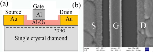
The fabrication process of the H-diamond MOSFETs was as follow. A 50 nm Au film was deposited by e-beam evaporation on the H-diamond surface. This Au layer was used as a sacrificial layer to protect the H-diamond away from resist and possible contamination or damage during the device fabrication process. The channel regions were defined by optical lithography. The Au sacrificial layer outside the channel regions was etched away by a KI/I2 solution. Then, device isolation was realized by oxygen plasma treatment. The source electrodes, drain electrodes, and gate pad electrodes were formed by lithography, Au metal evaporation, and lift-off. The source–drain spacing was defined by lithography, and the sacrificial layer of gold film on these regions was removed by KI:I2 solution wet etching. Al2O3 dielectric with thickness of 100 nm was deposited by an ALD process at 400 °C. After etching of Al2O3 dielectric on the source, drain, and gate pad electrodes, the gates were patterned by lithography. Al was deposited to form gate electrode. shows the cross-sectional schematic and scanning electron microscopy (SEM) image of the H-diamond MOSFET. The gate length of the fabricated H-diamond MOSFET is 0.9 μm. The source and drain space is 3 μm, with source-gate space LSG = 0.6 μm, and drain-gate space LDG = 1.5 μm.
Figure 1. (a) Cross-sectional schematic and (b) SEM image of the H-diamond MOSFET.
The direct current (DC) characteristics of the H-diamond MOSFETs were test by a semiconductor parameter analyzer. Small signal scattering (S) parameters measurement was carried out by a vector network analyzer with standard ground signal ground (GSG) probes. Continuous wave (CW) microwave power characteristics were measured on-wafer using an active load–pull system.
3. Results and discussion
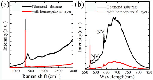
shows the Raman and photoluminescence (PL) spectra of the single crystal diamond substrate and that after homoepitaxial growth. As shown in , the Raman spectrum of the single crystal diamond substrate shows a sharp diamond Raman peak with the peak position of 1332.4 cm−1, and full width of half maximum (FWHM) of 3.9 cm−1. After homoepitaxial growth, the diamond Raman peak position is still 1332.4 cm−1, and the FWHM decreases to 2.7 cm−1, indicating the crystal quality of the single diamond is improved. For the single crystal diamond substrate, fluorescence effect induced by nitrogen impurities is obvious, and the nitrogen-vacancy (NV) center peaks are dramatic () due to the high nitrogen content of the diamond substrate. For homoepitaxial layer, the nitrogen impurity content decreases greatly, as indicated by the decrease of fluorescence effect. The nitrogen content is below 1 × 10¹⁶/cm3 by secondary ion mass spectroscopy (SIMS) measurement. Atomic force microscopy (AFM) measurement of the single crystal diamond after H2 plasma treated by the MPCVD shows a very smooth surface with surface roughness (RMS) of 0.43 nm in a region of 10 μm × 10 μm.
Figure 2. (a) Raman and (b) PL spectra of the single crystal diamond substrate and that after homoepitaxial growth.
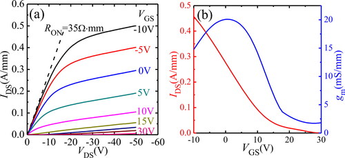
shows the current–voltage characteristics and transfer characteristics of the H-diamond MOSFET. The H-diamond MOSFET shows p type doping with the maximum drain saturation current of 500 mA/mm at the gate-source voltage VGS of −10 V, and the channel can be completely turned off at gate-source voltage VGS of 30 V. The on-resistance Ron is 35 Ω . mm for the H-diamond MOSFET. The source/drain ohmic contact resistance Rc measured by a transmission line method (TLM) is ∼3.2 Ω · mm, which indicates that a good ohmic contact is achieved. The high on-resistance Ron is mainly due to the high sheet resistance of the H-diamond material. The low carrier mobility is the limited factor for such high sheet resistance [Citation16]. Improvement of carrier mobility and the conductivity of the diamond channel has been the critical mission for developing of high performance diamond FETs. As shown in , the maximum transconductance gm reaches 20.1 mS/mm at VGS = 0 V and VDS = −30 V. The H-diamond MOSFET shows a high breakdown voltage of 121 V.
Figure 3. DC characteristics of the H-diamond MOSFET. (a) Current–voltage characteristics, and (b) transfer characteristics of the H-diamond MOSFET.
Capacity–voltage (C–V) characteristic of the H-diamond diode with 100 nm ALD Al2O3 dielectric was measured at 1 MHz, as shown in . The extracted forward and reverse flatband voltage of the device are 8.6 (VFB1) and 8.8 V (VFB2), respectively. The measured flatband voltages show positive shift compared with the theoretical flatband voltage (VFB0) of 0.62 V (calculated by the work functions of aluminum and H-diamond as 4.28 and 4.9 eV). It suggests that there are negative fixed charges existing in the interface of H-diamond and ALD Al2O3 dielectric layer, which helps to attract high density of holes to the H-diamond surface. The negative fixed charge density can be estimated by EquationEquation (1)(1)
(1) [Citation20]
(1)
(1)
Figure 4. (a) C–V characteristics of an H-diamond diode with 100 nm thick ALD Al2O3 dielectric measured at 1 MHz and (b) hole density with VGS.
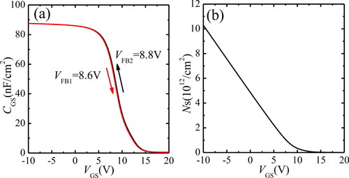
The calculated negative fixed charge density in the interface is 3.7 × 10¹²/cm2. The carrier density Ns of the 2DHG of H-diamond was calculated by ∫CGSdVGS, and the maximum carrier density Ns is 1.03 × 10¹³/cm2 at VGS = −10 V, as shown in . The linear tendency can be observed in the Ns–VGS curve, suggesting a relatively uniform carrier distribution in the 2DHG conduction channel of H-diamond.
Small hysteresis phenomenon was observed in the C–V characteristics of the H-diamond diode. The hysteresis value was 0.2 V. The presence of the hysteresis should be due to the injection of hole carriers into the ALD Al2O3 dielectric. The trapped charge density (Ntra) can be calculated by EquationEquation (2)(2)
(2) [Citation20]
(2)
(2)
The calculated trapped charge density in the ALD Al2O3 dielectric is 9 × 10¹⁰/cm2. The C–V characteristics show that the Al2O3 dielectric has a relative high quality [Citation21].
shows the high-frequency characteristics of a dual gate H-diamond MOSFET with gate length of 0.9 μm and gate width of 2 × 100 μm measured at VDS = −30 V, VGS = 9 V. The H-diamond MOSFET exhibits an extrinsic current gain cut-off frequency fT of 6.2 GHz and maximum oscillation frequency fmax of 17 GHz, respectively. The fT and fmax are reasonable values for the H-diamond MOSFETs with gate length of 0.9 μm [Citation22].
Figure 5. RF characteristics of the H-diamond MOSFET. (a) High-frequency characteristics |H21|2 and maximum available gain (MAG). RF power output characteristic of the H-diamond MOSFET measured under a continuous-wave signal at (b) 2 GHz, (c) 4 GHz, and (d) 10 GHz.
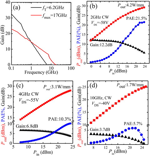
The RF power output characteristic of the H-diamond MOSFET was measured under a CW signal at 2, 4, and 10 GHz, as shown in . As shown in , benefit from the high quality Al2O3 dielectric, the drain work voltage reaches −58 V for the diamond MOSFET at 2 GHz. With VGS = 8 V, the maximum power gain, maximum CW output power density (Pout), and maximum power added efficiency (PAE) are 12.2 dB, 4.2 W/mm, and 21.5%, respectively. As shown in , at 4 GHz, with VDS = −55 V, the maximum power gain, maximum CW Pout, and maximum PAE are 6.8 dB, 3.1 W/mm, and 10.3%, respectively. As shown in , at 10 GHz, with VDS = −40 V, the maximum power gain, maximum CW Pout, and maximum PAE are 3.7 dB, 1.7 W/mm, and 5.7%, respectively.
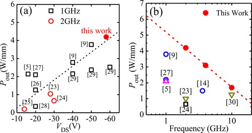
As shown in , the maximum output power density of 4.2 W/mm at 2 GHz, 3.1 W/mm at 4 GHz, and 1.7 W/mm at 10 GHz are all the highest output power densities obtained for H-diamond FETs [Citation14, Citation23–29]. The Pout can be estimated by
(3)
(3)
where IDS-max is the maximum drain current density, Vwork is the drain voltage for the measurement of Pout, and Vknee is the knee voltage. We think there are two main reasons for the good performances of the H-diamond MOSFET in this work. The first one is that the diamond is single crystal with high material quality and low surface roughness. Second, the diamond channel is passivated by the high quality ALD Al2O3 with low trapped charge density and negative fixed charge density in interface of the Al2O3 dielectric and H-diamond. As studied by Chen et al. [Citation30], trap effects are crucial for improving the performance of H-diamond MOSFETs. The drain current will be degraded by traps in both Al2O3 dielectric and diamond substrate. For the transistors working at high frequency and large power conditions, the trap effects would be more serious. The improvements of diamond substrate quality and the Al2O3 dielectric in this work are both beneficial for the improvement of output power characteristics of the H-diamond MOSFET.
Figure 6. Statistics of the output power characteristics for H-diamond MOSFET. (a) Statistics of the output power characteristics with work drain voltage at 1 and 2 GHz. (b) Statistics of the output power characteristics with frequency.
Compared with the widely used GaN HEMT [Citation31–33], the maximum PAE of the H-diamond MOSFET is low at now. The PAE is expressed as:
(4)
(4)
The H-diamond MOSFET is working as a Class A mode, for which the PAE is limited to 50%. There are some reasons for the relatively low PAE of the H-diamond MOSFET. The most important reason is that the sheet resistance of the H-diamond channel is high and the carrier mobility is low. At the same time, the ohmic contact resistance is high for the diamond FETs. The above reasons make the parasitic resistance is very high for the H-diamond MOSFET. In this work, the parasitic resistance is about 10× higher than that of GaN HEMTs, which was caused by higher sheet resistance and higher ohmic contact resistance. The large parasitic resistance will produce Joule’s heat and limit the Pout and PAE of the H-diamond MOSFETs. The large sheet resistance and ohmic contact resistance also make the drain saturation current is low and the knee voltage is high, which also limited the Pout and PAE of the H-diamond MOSFETs (EquationEquation (3)(3)
(3) ). The second reason is that the maximum oscillation frequency fmax is relatively low, which limites the gain of H-diamond MOSFET. The low gain makes the PAE is low. The maximum oscillation frequency is influenced by many factors, including the parasitic parameters, the gate length, and gate dielectric thickness. The structure of the H-diamond MOSFETs needs to be improved further.
The maximum CW output power density (Pout) and maximum PAE for our H-diamond MOSFET are lower than the GaN HEMT devices mainly due to the imperfect electrical properties of the diamond channel at now. But the large heat dissipation demand and high junction temperature have been the limited factors for the GaN HEMT devices for high frequency and high power application. Diamond possesses perfect thermal conductivity, which make it more suitable for application in high frequency and high power area. Improvements of electrical properties and device structure of the diamond FETs will make them play an important role in the future.
4. Conclusion
In summary, H-diamond MOSFETs with ALD Al2O3 as gate dielectric were fabricated on (0 0 1) single crystal diamond to optimize the high frequency and high power characteristics. The H-diamond MOSFETs possess good ohmic contact and high quality Al2O3 gate dielectric. The H-diamond MOSFET with gate length of 0.9 μm and Al2O3 gate dielectric of 100 nm shows maximum drain saturation current of 500 mA/mm, maximum transconductance of 20.1 mS/mm. Due to the high quality diamond substrate and gate dielectric, the drain work voltage of the H-diamond MOSFET reaches −58 V, and a maximum CW output power density of 4.2 W/mm at 2 GHz is obtained. The CW output power density of 3.1 W/mm at 4 GHz and 1.7 W/mm at 10 GHz are obtained at the same time. The results show the application promising of H-diamond FETs on (0 0 1) single crystal diamond for high frequency and high power electronics.
Disclosure statement
No potential conflict of interest was reported by the authors.
Additional information
Funding
References
- Wort CJH, Balmer RS. Diamond as an electronic material. Mater Today. 2008;11(1–2):22–28.
- Yamasaki S, Gheeraert E, Koide Y. Doping and interface of homoepitaxial diamond for electronic applications. MRS Bull. 2014;39(6):499–503.
- Kawarada H, Aoki M, Ito M. Enhancement mode metal-semiconductor field effect transistors using homoepitaxial diamonds. Appl Phys Lett. 1994;65(12):1563–1565.
- Hirama K, Sato H, Harada Y, et al. Diamond field-effect transistors with 1.3 a/mm drain current density by Al2O3 passivation layer. Jpn J Appl Phys. 2012;51:090112.
- Kasu M, Ueda K, Ye H, et al. 2W/mm output power density at 1 GHz for diamond FETs. Electron Lett. 2005;41(22):1249–1250.
- Nebel CE, Rezek B, Zrenner A. Electrical properties of the 2D-hole accumulation layer on hydrogen terminated diamond. Diamond Relat Mater. 2004;13(11–12):2031–2036.
- Landstrass MI, Ravi KV. Hydrogen passivation of electrically active defects in diamond. Appl Phys Lett. 1989;55(14):1391–1393.
- Grot SA, Gildenblat GS, Hatfield HCW, et al. The effect of surface treatment on the electrical properties of metal contacts to boron doped homoepitaxial diamond film. IEEE Electron Device Lett. 1990;11(2):100–102.
- Imanishi S, Horikawa K, Oi N, et al. 3.8 W/mm RF power density for ALD Al2O3-based two-dimensional hole gas diamond MOSFET operating at saturation velocity. IEEE Electron Device Lett. 2019;40(2):279–282.
- Yu C, Zhou CJ, Guo JC, et al. 650 mW/mm output power density of H-terminated polycrystalline diamond MISFET at 10 GHz. Electron Lett. 2020;56(7):334–335.
- Ueda K, Kasu M, Yamauchi Y, et al. Diamond FET using high-quality polycrystalline diamond with fT of 45 GHz and fmax of 120 GHz. IEEE Electron Device Lett. 2006;27(7):570–572.
- Zhou CJ, Wang JJ, Guo JC, et al. Radiofrequency performance of hydrogenated diamond MOSFETs with alumina. Appl Phys Lett. 2019;114(6):063501.
- Jingu Y, Hirama K, Kawarada H. Ultrashallow TiC source/drain contacts in diamond MOSFETs formed by hydrogenation-last approach. IEEE Trans Electron Device. 2010;57(5):966–972.
- Kudara K, Imanishi S, Hiraiwa A, et al. High output power density of 2DHG diamond MOSFETs with thick ALD-Al2O3. IEEE Trans Electron Device. 2021;68(8):3942–3949.
- Kudara K, Arai M, Suzuki Y, et al. Over 1 A/mm drain current density and 3.6 W/mm output power density in 2DHG diamond MOSFETs with highly doped regrown source/drain. Carbon. 2022;188:220–228.
- Yamada H, Chayahara A, Mokuno Y, et al. A 2-in. mosaic wafer made of a single-crystal diamond. Appl Phys Lett. 2014;104(10):102110.
- Kim SW, Kawamata Y, Takaya R, et al. Growth of high-quality one-inch free-standing heteroepitaxial (0 0 1) diamond on (11–20) sapphire substrate. Appl Phys Lett. 2020;117(20):202102.
- Schreck M, Gsell S, Brescia R, et al. Ion bombardment induced buried lateral growth: the key mechanism for the synthesis of single crystal diamond wafers. Sci Rep. 2017;7:44462.
- Wang JJ, He ZZ, Yu C, et al. Comparison of field-effect transistors on polycrystalline and single-crystal diamonds. Diamond Relat Mater. 2014;43:43–48.
- Schroder DK. 2006. Semiconductor material and device. New York: Wiley. (Sect. 6.2).
- Saha NC, Kasu M. Heterointerface properties of diamond MOS structures studied using capacitance–voltage and conductance–frequency measurements. Diamond Relat Mater. 2019;91:219–224.
- Chen ZH, Fu Y, Kawarada H, et al. Microwave diamond devices technology: field-effect transistors and modeling. Int J Numer Model El. 2021; 34(3): 2800.
- Yu XX, Hu WX, Zhou JJ, et al. 1 W/mm output power density for H-terminated diamond MOSFETs with Al2O3/SiO2 bi-layer passivation at 2 GHz. IEEE J Electron Device Soc. 2020;99:1.
- Ivanov TG, Wei J, Shah PB, et al. Diamond RF transistor technology with ft = 41 GHz and fmax = 44 GHz. IEEE/MTT-S International Microwave Symposium. 2018. p. 1461.
- Camarchia V, Cappelluti F, Ghione G, et al. RF power performance evaluation of surface channel diamond MESFETs. Solid State Electron. 2011;55(1):19–24.
- Kasu M, Ueda K, Ye H, et al. High RF output power for H-terminated diamond FETs. Diamond Rel Mater. 2006;15(4–8):783–786.
- Hirama K, Takayanagi H, Yamauchi S, et al. High-performance p-channel diamond MOSFETs with alumina gate insulator. IEEE International Electron Devices Meeting. 2007. p. 873.
- Kubovic M, Kasu M, Kallfass I, et al. Microwave performance evaluation of diamond surface channel FETs. Diamond Rel Mater. 2004;13(4–8):802–807.
- Yu X, Hu W, Zhou J, et al. 1.26 W/mm output power density at 10 GHz for Si3N4 passivated H-terminated diamond MOSFETs. IEEE Trans Electron Device. 2021;68(10):5068–5072.
- Chen Z, Yu X, Zhou J, et al. Characterization of substrate-trap effects in hydrogen-terminated diamond metal-oxide-semiconductor field-effect transistors. IEEE Trans Electron Device. 2022;69(1):278–284.
- Wu Y, Moore M, Saxler A, et al. 40 W/mm double field-plated HEMTs. 2006 64th Device Research Conference. 2006. p. 151–152.
- Tadjer M, Anderson T, Ancona M, et al. GaN-on-diamond HEMT technology with TAVG = 176 °C at PDC,max = 56 W/mm measured by transient thermoreflectance imaging. IEEE Electron Device Lett. 2019;40(6):881–884.
- Ohki T, Yamada A, Minoura Y, et al. An over 20-W/mm S-band InAlGaN/GaN HEMT with SiC/diamond-bonded heat spreader. IEEE Electron Device Lett. 2019;40(2):287–290.