
 ?Mathematical formulae have been encoded as MathML and are displayed in this HTML version using MathJax in order to improve their display. Uncheck the box to turn MathJax off. This feature requires Javascript. Click on a formula to zoom.
ABSTRACT
A design strategy is proposed for microwave devices built with dielectric-loaded waveguides having one- or two-dimensional discontinuity profiles. The problem is formulated as an inverse problem where the pre-defined scattering parameters are aimed to be the final response of the system. This goal is achieved by optimizing the dimensions of the filling materials. To increase the success of the optimization, the problem is reduced to the longitudinal and widthwise thickness determination of the unit cell, which constitutes the whole structure in a cascade form. To this aim, the frequency response of the unit cell is targeted and then that of the whole system, which is achieved by a two-level optimization procedure of the unit cell. The usefulness of the proposed design strategy is shown through numerical examples as well as the measurement results of two prototypes.
1. Introduction
Waveguides are popular microwave devices in satellite communication, military applications, etc., due to their high-power handling capacity, high-quality factor, and low-loss features [Citation1]. Microwave passive devices utilizing waveguide structures are first designed by corrugating the cross-sectional shape [Citation2,Citation3] or inserting metal discontinuities in the waveguide [Citation4]. Since waveguides are mainly preferred for high-frequency applications, minor faults in the fabrication process may drastically affect the operation properties of the device. One another reason for operating waveguides in microwave systems is their high-power handling ability. Therefore, the breakdown voltage of hollow waveguides may cause problems in some high-power applications. Besides, waveguide devices with a corrugated shape or metallic inserts have a bulky and heavy geometry. A possible solution to overcome drawbacks of the corrugated or metal inserted hollow waveguide structures is to fill the apparatus with dielectric materials, which provide reduced size devices with a high breakdown voltage [Citation5,Citation6]. However, difficulties due to the fabrication process of the metallic parts remain in this design solution. Because of the aforementioned facts, uniform waveguides with dielectric loading may propose a possible and efficient solution to the design of waveguide-based microwave devices. Yet, there is rare literature on practically realizable microwave devices built by dielectric-loaded uniform waveguides (DLW). DLW structures can be classified in terms of modal interaction and dielectric discontinuity [Citation7]. Longitudinally inhomogeneous waveguides (LIW) and widthwise and longitudinally inhomogeneous waveguides (WLIW) are two possible DLW configurations in terms of modal interaction, for which the electrical discontinuity exists only in the longitudinal direction and both in widthwise and longitudinal directions, respectively.
In [Citation8–12], several LIW structures are optimized for both permittivity and thickness values of layers to propose various microwave devices such as filters, phase shifters, and impedance matching sections. In [Citation12], the determination of the electrical and the geometrical profile is provided by assuming a longitudinally layered dielectric profile where the permittivities of only some layers are pre-chosen. The permittivity values are then determined for the rest of the structure as well as the thickness values of all layers utilizing the classical Chebyshev filter design [Citation13,Citation14]. Although this approach allows the use of commercially available materials at some parts of the design, the designed permittivity profile for the other parts stands as the main drawback of the proposed method for practicability issues since determining the permittivity is not a practically realizable attempt due to the current material technology. In [Citation15], a synthesis method for microwave filters based on the determination of passband points of a dielectric-loaded waveguide with an infinite periodicity is introduced for WLIW type structures. However, modelling the ultimate infinite design by a finite structure still requires plenty of cascaded cells which finally form a bulky and redundant design. In [Citation16,Citation17], a mode-matching method is integrated as an electromagnetic (EM) solver into an evolutionary optimization technique for the synthesis of a phase shifter in WLIW form. To the best of our knowledge, the literature for DLW-based microwave devices is lacking and open to the contributions regarding the advantages of these types of structures and the mentioned disadvantages of the readily available methods. In this study, we intend to contribute to this gap by proposing a methodological approach for the synthesis of practically realizable LIW- and WLIW-based compact microwave devices. Previously, in [Citation18], we have shown that the optimization success of a LIW drastically decreases as the number of layers increases, and the success of the iterative optimization becomes highly dependent on the appropriate choice of initial values as it is expected due to the nature of the ill-posed nature of the inverse problems. To remedy this issue, we have proposed to use an approximate reflection coefficient of the multi-layer structure by regarding the first reflected and transmitted waves at each layer so that the initial values are generated by solving the approximated under-determined system in the manner of an approximate inverse problem instead of assigning random or arbitrarily chosen initial values [Citation19]. Note that the approximate analytical determination of initial values in [Citation19] is only capable of determining the thickness values of a few-layered LIW from its offcast frequency response and cannot be applied directly and reliably for LIW-based microwave devices, which requires a plenty number of layers to generate a frequency response with abrupt variations as in [Citation18]. Therefore, ingenious enhancements are required for the synthesis of practical microwave devices, which cannot be provided by a trial and error-based approach as in [Citation18]. Along these lines, in this study, we propose to divide the whole structure into equal unit cells on which the optimization process is carried out on a less amount of variables for the promise of a better optimization result. A readily available function in MATLAB software, TR, a subspace trust-region based, non-linear, least-squares and iterative optimization method [Citation20,Citation21], is used as the optimization tool. Before the optimization process, the appropriate frequency response of the unit cell is chosen from a set of possible solutions concerning that of the whole system. At the first step of optimization, the unit cell is optimized by targeting the chosen appropriate frequency response of the unit cell, where approximate analytical initial values are used. A second step is then applied in the optimization routine to increase the success of optimization, where the optimized values of the unit cell obtained at the first step are assigned as the initial values for the second step and the new targeted response is set as the whole structure. This two-level optimization procedure provides a methodological design process by considering the frequency response of the unit cell and cascaded structure sequentially.
Although the proposed two-level optimization procedure is directly applicable to LIW structures, there can be problems in the practical implementation of such structures due to the fabrication process. LIW structures require the use of more than one material and layers to be prepared one by one. Preparation of the whole structure is cumbersome and prone to cutting errors which affect the frequency response adversely. Besides, the mechanical stability of the structure is another issue to be tackled. Therefore, a design possibility with WLIW structures, which also enables the use of one single type of material, is also proposed to solve these drawbacks. However, the large size of the structure may give a costly and burdensome computational task if one integrates the chosen EM solver for the frequency analysis of WLIW into the optimization process. Hence, the structure is formed by cascaded equal cells as in the previous design possibility, but this time the modal interaction between propagating and evanescent modes should be regarded to obtain the frequency response of the whole structure. Regarding these points, the LIW model of the WLIW structure is constructed through effective medium theory (EMT), and optimization of WLIW is carried out on the equivalent LIW structure. Note that the thickness values of cascaded layers with pre-chosen dielectric values are optimized to minimize the error between pre-defined scattering parameters and the ones obtained by the designed LIW or WLIW structure. Therefore, the proposed reverse design procedure is considered as an inverse problem. Inverse problems which are generally formulated for the determination of electrical properties of dielectric obstacles located in rectangular waveguides has a vast literature [Citation22–30]. In such problems, a unique solution as the detection of the unique scattering properties (e.g. the dielectric permittivity of the obstacle) is the primary target [Citation31] while the existence problem is thoroughly examined [Citation32]. On the contrary, we propose a synthesis strategy that aims for a possible spatial variation of the dielectric loading in a manner of an inverse problem. Therefore, the uniqueness of the solution is not a considered issue since one aims to satisfy the optimization criteria for such design purposes as in [Citation33] and there can be several solutions on the search path of the optimization routine. On the other hand, since the synthesis is optimization-based, the minimization of the cost function is the main target and the existence of the exact solution guaranteeing the cost function to be zero is out of the interest of the strategy. Design solutions formulated in the manner of an inverse problem in modern engineering approaches follow similar strategies [Citation33–39]. For the minimization of the cost function, the designer's experience becomes a robust tool to guess whether a desired solution exists for the given problem. A search routine may be added to the proposed algorithm where a set of different materials can be assigned one by one to expand the optimization space at the cost of additional computation.
Throughout the paper, the forward problem in the frequency analyses during the optimization procedures are carried out via a well-known mode-matching method as applied in [Citation18]. In this study, microwave filters are selected for the implementation of the proposed methods. Since these methods are based on formulating the synthesis problem of LIW and WLIW structures as an inverse problem by targeting the pre-defined frequency response, they have the potential to be applied to different types of microwave devices, of which the device parameters are defined in terms of scattering parameters such as phase shifters, antenna feeds, impedance matching devices, etc. The efficiency and accuracy of the proposed approach are first shown through numerical examples and then tested by the measurement of fabricated prototypes for both LIW and WLIW structures. It has been observed that the proposed methods give good accuracy for experimental cases as well as numerical examples.
2. Statement of the problem
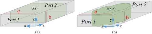
The geometries of considered problems are given in Figure . Dielectric permittivity variation has inhomogeneity only in the longitudinal direction in Figure (a) and both in widthwise and longitudinal directions in Figure (b). In this study, the dielectric materials are pre-defined and the spatial variation is the inquiry. LIW structures are composed of different materials and WLIW structures are composed of one chosen material.
Figure 1. Illustrations of (a) LIW, (b) WLIW.
Assume that following are given:
| – | Scattering parameters at | ||||
| – | Dielectric permittivity of the materials. | ||||
| – | The spatial order of the used materials (For LIW). | ||||
The aim of the LIW problem is
| – | To determine the thickness layers of dielectric materials in the longitudinal direction, and the aim for the WLIW problem is | ||||
| – | To determine the thickness of dielectric material in the longitudinal and widthwise directions through the whole system. | ||||
3. Design strategies
In the following subsections, the design strategies are introduced. In Section 3.1, an approach to obtain the scattering parameters of a multi-layered unit cell from the frequency response of the whole system is explained so that the identical multi-layered unit cell is optimized instead of the whole structure to increase the solidity of the optimization routine. Then a two-level optimization procedure is applied to determine the thickness values of each layer in the unit cell. The first step of the optimization routine is introduced in Section 3.2. In Section 3.3, the second step, which is applied to ameliorate the optimization routine, is explained. In Section 3.4, mapping the physical properties of a WLIW structure into those of a LIW structure is explained. Note that further steps are common for both the design of LIW and WLIW structures, except Section 3.4.
3.1. Identical multi-layered unit cell approach
A LIW structure is a two-port network for which the conversion between S-parameters and T-parameters is valid [Citation40].
The first step for the optimization of the proposed design strategy is given step by step below.
Step 1: Convert S-parameters, S, of the whole structure to its T-parameters [Citation40].
Step 2: T-matrix () of the whole structure, which is assumed to be composed of cascaded N identical unit cells, can be calculated as
(1)
(1) where
is the T-matrix of each identical unit cell. Reversely, one may calculate the T-matrix of the identical unit cell
as given in (Equation2
(2)
(2) ) through
obtained in step 1
(2)
(2) where
is constituted of complex variables. Therefore, Nth root of
can be calculated as in (Equation3
(3)
(3) ) through Jordan decomposition,
(3)
(3) where P and R are the matrices, consist of eigenvectors and eigenvalues of
, respectively.
Step 3: Obtain elements of scattering matrix of the multi-layered unit cell () using the conversion from T parameters to S parameters [Citation40].
Since R in (Equation3(3)
(3) ) is a diagonal complex matrix, Nth root operation results in
solutions. Obtained solutions can be eliminated regarding the description of the considered problem. Assuming that lossless dielectric discontinuities are used in the filter design, the mathematical solution pairs for
and
are eliminated, including (i) the non-physical pairs satisfying
(ii) pairs with the non-physical solutions
and/or
. Following that, the candidate scattering parameters are cascaded and the pairs resulting least magnitude difference with that of the desired response of the whole structure are chosen as the response of the identical multi-layered unit cell for each frequency. The first step of the two-level optimization procedure, which is named reverse optimization (RO), is explained in the following section.
3.2. Reverse optimization
TR necessitates initial values as other iterative optimization approaches. To generate feasible initial values, the total reflection (i.e. ) of the multi-layered dielectric structure in the waveguide is roughly approximated. Track of the main reflected and transmitted waves is depicted in Figure . The thickness of the layers are candidate initial values for TR procedure and represented with
, where subscript n is the layer number and
denotes the dielectric permittivity of the nth layer.
Figure 2. Track of main reflections and transmissions for multi-layer structure [Citation19].
![Figure 2. Track of main reflections and transmissions for multi-layer structure [Citation19].](/cms/asset/9fd484c1-f507-400c-82c9-51cdadc9de54/gipe_a_2081321_f0002_ob.jpg)
In Figure , represents the reflection coefficient between
th and nth layers and
, where
is the propagation constant of the nth layer. Summing the main reflections, one obtains the approximated total reflection for each frequency as
(4)
(4) Here, one finally aims to determine
values embedded in
values by increasing the amount of data by applying (Equation4
(4)
(4) ) with different frequency values. Note that the accuracy of this approximation decreases as the number of layers increases. Then, (Equation4
(4)
(4) ) is rearranged in an matrix equation to obtain unknown
values in
term as
(5)
(5) where the constant matrix
is composed of the difference between the desired
and first reflection
values at M frequency values and the explicit expression for
is
(6)
(6) Regarding (Equation4
(4)
(4) ) and (Equation5
(5)
(5) ), the elements of coefficient matrix
are
(7)
(7) where
,
,
is the pth frequency, and the layer number s is
(8)
(8) and the elements of the unknown column matrix
are
(9)
(9) where
is the frequency index while ‘
’ operator rounds its argument to the upper integer. Note that
is related to the summation of
values, which is a function of the operating frequency, thickness value, and the dielectric permittivity of the nth layer. Therefore, the number of unknown values for
increases from N to
through (Equation4
(4)
(4) ) due to the frequency dependency of
values. Hence, the resultant system of linear equations in (Equation4
(4)
(4) ) forms an under-determined matrix equation and a possible solution of the constructed system (Equation5
(5)
(5) ) can be obtained as
(10)
(10) where † is the pseudo-inverse operator. Once the column vector
is determined via (Equation10
(10)
(10) ) while its rows are essentially in the form of (Equation9
(9)
(9) ), it can be decomposed as
following simple element-wise division between columnsFootnote1 and expressing
Footnote2In this study, MATLAB software was used for calculations where the range for
and
is, respectively, set as
and
by default. Let the exponential term
, where k is the number of half periods of the
. For given ranges of inverse cosine and inverse sine functions, using the relation for any given
,
(11)
(11) one can relate
(12)
(12) and
(13)
(13) where
rounds its argument to the lower integer so
is obtained and the most right-hand side term ξ in (Equation13
(13)
(13) ) is
(14)
(14) If one knows k, then
values can be simply calculated via (Equation13
(13)
(13) ). However, only the ξ value is attainable and
is inherently elusive. A primitive yet a fast parameter sweep is carried out to obtain a coherent k value. Having generated randomly in the optimization interval (i.e.
while
and
are chosen regarding the physical availability for manufacturing and the guided wavelength of operating frequency band, respectively),
vectors are used to determine candidate
for each layer and frequency by solving
(15)
(15) where
is the only unknown term. Candidate
thickness values of sth layer are simply determined for each frequency. Finally, M (the total number of frequencies) different
values for each layer are averaged over frequency by simply ignoring any imaginary part if exists as
(16)
(16) to obtain
values which are physically possible. Note that in (Equation15
(15)
(15) ),
values are generated randomly in a large amount (e.g. in this study 1000 vector are generated), so this amount of
are generated. The initial values are chosen from calculated
length vectors by calculating the minimum error via the defined error function E.F.
(17)
(17) where U and O stand for the desired frequency response of the unit cell,
, and the frequency response of the candidate
length vector, respectively. Here, subscripts 11 and 21 denote for the reflection and transmission coefficients, respectively. After initial values InVal are set from
vectors as the one having the minimum E.F. in (Equation17
(17)
(17) ), thickness values
of the layers in unit cell are optimized with initial values InVal subject to constraints
. This procedure is called as RO and (Equation17
(17)
(17) ) is utilized as the error function in RO as well, where U and O stand for the desired frequency response
and the frequency response of each iteration step in the TR optimization routine, respectively.
In the following part, an additional optimization step is explained for ameliorating the vector, which is named forward optimization (FO).
3.3. Forward optimization
In RO, the targeted frequency response is assigned as that of the unit cell as explained in Section 3.2. To enhance the values, FO is applied as a second optimization step, in which the target of the optimization is assigned as the S-parameters of the whole structure. In FO, the initial values are chosen as
values obtained in the RO step. It is expected that the final optimization results
to vary around
. Hence, the bounds of the optimization space are chosen subject to
. The same objective function in (Equation17
(17)
(17) ) is used by assigning the arguments U and O as the desired and being optimized S parameters of the cascaded (whole) structure, respectively. The S parameters for the whole system in each optimization step are calculated via cascading the current S parameters of the unit cells. There are several methods to obtain the frequency response of a LIW such as utilizing ABCD matrices [Citation8], Method of Moments [Citation41], and in this study, a generalized scattering matrix approach [Citation42] is utilized where only the self-interaction of the dominant mode is regarded via mode-matching method as applied in [Citation18]. Note that all aforementioned steps are common both in the design of LIW and WLIW structures. The following part exclusively concerns the design strategy of WLIW structures.
3.4. LIW equivalence of WLIW
Due to the computational burden in the calculation of the frequency response of WLIW structures, it is proposed to optimize the thickness values of layers in LIW equivalence. The equivalence between the two structures is constructed via the EMT and the equivalent LIW is illustrated in Figure together with corresponding WLIW for both cross-sectional and longitudinal views, where stands for the permittivity of free space. Note that the success of the EMT decreases as w/a decreases due to the increasing dominance of higher-order modes. In our case, the equivalence approach is convenient and functional as we require high dielectric contrast between layers which can be provided with high w/a ratios.
Figure 3. Illustrations of equivalence LIW (left) and WLIW (right). (a) Cross-sectional view. (b) Longitudinal view.
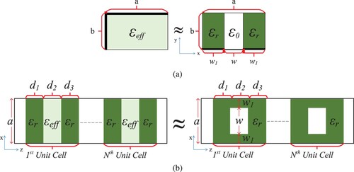
EMT assumes that the effective dielectric permittivity fills the entire cross-section and propagation of only the dominant mode is regarded. Simply arranging the relation between
and propagation constant β in the
loaded waveguide, one can obtain
(18)
(18) where
and λ are the propagation constant and the wavelength in the free-space which are known for the given frequency. Hence,
can be obtained by first determining β for the given configuration in Figure as explained in [Citation43].
The design strategy is summarized below step by step, for the sake of clarity. Note that if one aims to design a WLIW structure using LIW equivalence, the proposed mapping can be applied as an initial step.
Step 1: Obtain the frequency response of the identical unit cell, (see Section 3.1).
Step 2: Determine the initial values InVal for RO step (see Section 3.2).
Step 3: Optimize thickness values of the layers in the identical unit cell w.r.t. (i.e. RO step) (see Section 3.2).
Step 4: Optimize thickness values of the layers in the identical unit cell by targeting the frequency response of the whole system, S (i.e. FO step) (see Section 3.3).
4. Design examples
A WR-90 waveguide is operated in the dominant mode region between 8 and 12 GHz and the measurement system is calibrated with SOLT (short-open-load-thru) procedure. The desired magnitude responses are generated using given data in [Citation12] for Design 1 and AWR for Design 2. The phase data are generated by assuming that assigned layers have a constant thickness (which are chosen as 4 mm, approximately equal to at the centre frequency where
is the guided wavelength of the hollow waveguide for all examples) for corresponding LIW structure with the chosen dielectric profile. Then, the desired frequency response is formed by combining the desired magnitude response and calculated phase data. In all examples, the frequency band is divided into M = 120 equispaced points. For the design of LIW structures, the procedure explained from Sections 3.1 to 3.3 is followed. The lower (
) is assigned as 1 mm regarding the manufacturability, and the upper (
) bound is assigned as 10 mm, approximately corresponds to
in the mid of the interested band. The same procedure is performed for the design of WLIW structures following the establishment of the LIW equivalence as explained in Section 3.4. Note that LIW equivalence has frequency-dependent permittivity values for partially filling parts of WLIW (i.e. illustrated with width
in Figure ) and
monotonically decreases with increasing frequency. Hence,
is assigned as to that of the mid-frequency value in the analysis and design band, which is particularly 10 GHz in the following designs. Thereafter, the same design procedure (i.e. from Sections 3.1 to 3.3) is applied to the LIW equivalence of WLIW. One another design consideration is a proper choice of the number of unit cells. In this study, N + 1 unit cells are cascaded for a given Nth degree filter which is inspired by the filter design introduced in [Citation13] where N + 1 impedance inverters and N series resonators are used for a Nth degree Chebyshev filter. A rigorous investigation is carried out to select the appropriate amount of unit cells. It is observed that cascading any number of unit cells instead of N + 1 for an interested Nth degree filter gives comparatively inefficacious results due to the inherent behaviour of unit cells. This tendency of the structures is explained along with numerical examples as a further investigation. Besides, the unit cells are composed of three layers both for the purposes of having a compact design in size and increasing the accuracy of the initial value problem. Table summarizes the determined length values of the unit cell in the longitudinal direction for each step of the design procedure and considered examples. The final responses of the designed structures are validated by high-frequency structure simulator (HFSS) [Citation44] which is a finite element method-based EM solver.
Table 1. Optimized thickness values and total lengths.
In the first example, a 3rd order Chebyshev-like bandpass filter with 0.9 GHz bandwidth around the centre frequency 10 GHz and ripples around 0.5 dB [Citation9,Citation12] is considered as Design 1. Regarding the relatively narrow bandwidth, a three-layered unit cell with high contrast dielectric profile is chosen for design goals and N = 4 unit cells are cascaded for the 3rd order filter. The air-gap ratio is obtained as
in WLIW for modelling the lower dielectric value in
(i.e.
at 10 GHz) with respect to the higher value in
(i.e.
) as shown in Figure (a). For clarity, the magnitude variation results for each strategy are explicitly shown in Figure . The chosen frequency response,
, for the given unit cell configuration, is determined as explained in Section 3.1. Afterwards, the RO step is applied for the chosen
as explained in Section 3.2. The frequency response for
and RO solutions are plotted for magnitude values in Figure (b). In Figure (c), the cascaded response of the RO approach is given together with the desired response of the whole structure, for which a non-negligible discrepancy exists. To ameliorate the results obtained via RO, FO is applied as explained in Section 3.3. In Figure (d), enhanced results after applying FO are given with the label FO-LIW. The same design steps are also applied for a WLIW structure, by first constructing its LIW equivalence as explained in Section 3.4. The frequency response of the designed WLIW structure is then simulated in HFSS and the results are plotted in Figure (d) as well, together with an inset showing 3 dB bandpass behaviour for the sake of clarity. One can observe that the frequency responses of both LIW and WLIW structures are in close proximity to the desired response after the FO step is applied. Note that the partially filling parts are first modelled via EMT. Then LIW equivalence of WLIW is optimized for which the intermediate steps are not plotted in Figure (b,c) for brevity. The thickness values of both WLIW and LIW designs are listed in Table . It is observed that examined periodic structures produce frequency responses in a similar form of Chebyshev type, where the explicit discrepancy between the desired and designed responses in logarithmic scale occurs only for values below −15 dB, which is not significant for filter design purposes.
Figure 4. Design 1 Chebyshev filter with 0.9 GHz bandwidth and 0.5 dB ripple . (a)
vs w/a and
vs frequency (inset), (b) unit cell responses of chosen
, RO, (c) cascaded response of RO, (d) responses for the whole structure (final responses). RO: reverse optimization; FO: forward optimization.
![Figure 4. Design 1 Chebyshev filter with 0.9 GHz bandwidth and 0.5 dB ripple εuc=[151.0315]. (a) εeff vs w/a and εeff vs frequency (inset), (b) unit cell responses of chosen Suc, RO, (c) cascaded response of RO, (d) responses for the whole structure (final responses). RO: reverse optimization; FO: forward optimization.](/cms/asset/75afda4b-ed15-4674-8e72-c7762e0e3457/gipe_a_2081321_f0004_oc.jpg)
To show the suitability of the number of unit cells, designs with cascading N = 3 and N = 5 unit cells are also examined. In Figures (a) and (b), N = 3 and N = 5 unit cells, respectively, form the whole device and as expected, the discrepancy between the targeted and designed responses widens. Also, designs with different materials are examined both to show the adequacy of the proposed method and that different designs are possible. In Figures (c) and (d), N = 4 unit cells composed of and
are assigned, respectively, and the trend of the targeted response is accomplished with better outcomes especially in the bandpass region compared to designs with N = 3 Figure (a) and N = 5 Figure (b).
Figure 5. Design 1 with different number of unit cells N or materials. (a) and
(b)
and N = 5, (c)
and N = 4, (d)
and N = 4.
![Figure 5. Design 1 with different number of unit cells N or materials. (a) εuc=[151.0315] and N=3, (b) εuc=[151.0315] and N = 5, (c) εuc=[131.0313] and N = 4, (d) εuc=[171.0317] and N = 4.](/cms/asset/b483060b-6d6c-40ad-bf09-d34c0e6babdc/gipe_a_2081321_f0005_oc.jpg)
Another example is devoted to testing the abilities of the proposed method against a different type of filter and higher bandwidth. To this aim, a 5th order elliptical bandpass filter with 1.5 GHz bandwidth and equal ripples of 0.05 dB is targeted. To achieve a wider passband as to Design 1, the contrast of the dielectric profile is smoothed and chosen as and N = 6 unit cells are cascaded for the 5th order filter. The air-gap ratio is obtained as
as shown in Figure (a) and for explicitness, frequency responses related to all optimization stages are plotted in Figure . A good agreement between the desired and designed responses can be observed in Figure (d), where the frequency response of the WLLIW structure is simulated via HFSS and the 3 dB bandwidth region is given as an inset for more clear observation. The thickness values for each design step are also given in Table . As in Design 1, one can see that a close agreement exists between the frequency responses of LIW and WLIW structures. Note that due to the nature of the cascaded system, the frequency response of the design has a Chebyshev-like behaviour, yet it is in a very close agreement with the desired one, except for values below −30 dB, which does not affect the filter expectations adversely. Designs with cascading N = 5 and N = 7 unit cells are also examined to demonstrate the feasibility of the number of unit cells. In Figures (a) and (b), N = 5 and N = 7 unit cells form the entire device, respectively, and the gap between the targeted and designed responses increases as expected. Additionally, designs with various materials are examined to demonstrate the efficacy of the suggested technique and that the technique is not strictly limited by the issue of existence. Figures (c) and (d) show N = 6 unit cells composed of
and
, respectively, and the tendency of the targeted response is achieved with better effectiveness, particularly in the bandpass region, when compared to designs with N = 5 Figures (a) and N = 7 Figure (b).
Figure 6. Design 2 elliptic filter with 1.5 GHz bandwidth and 0.05 dB ripple . (a)
vs w/a and
vs frequency (inset), (b) unit cell responses for chosen
, RO, (c) cascaded response of RO, (d) responses for the whole structure (final responses). RO: reverse optimization; FO: forward optimization.
![Figure 6. Design 2 elliptic filter with 1.5 GHz bandwidth and 0.05 dB ripple εuc=[91.039]. (a) εeff vs w/a and εeff vs frequency (inset), (b) unit cell responses for chosen Suc, RO, (c) cascaded response of RO, (d) responses for the whole structure (final responses). RO: reverse optimization; FO: forward optimization.](/cms/asset/a936eb7d-9b58-4212-9577-d1ac8c9dab87/gipe_a_2081321_f0006_oc.jpg)
Figure 7. Design 2 with different number of unit cells N or materials. (a) and
(b)
and N = 7, (c)
and
(d)
and N = 6.
![Figure 7. Design 2 with different number of unit cells N or materials. (a) εuc=[91.039] and N=5, (b) εuc=[91.039] and N = 7, (c) εuc=[81.038] and N=6, (d) εuc=[101.0310] and N = 6.](/cms/asset/c4d129cc-350a-4bfe-916f-6be0594215f8/gipe_a_2081321_f0007_oc.jpg)
The last examples are devoted to validating the proposed method with real measurement data. A design scenario is carried out with FR4 material, which is, in fact, not suitable for filter design purposes due to the non-negligible losses but the available substance in hand. Regarding the low permittivity of FR4, a wide-band filter is considered which is a 3rd order Chebyshev bandpass filter with 1.65 GHz bandwidth and equal ripples of 0.01 dB. The three-layered unit cell is cascaded N = 4 times for the targeted 3rd order filter and has a dielectric profile of where the real part operator
stands for ignoring the losses of FR4 material during the design procedure and
represents the relative complex permittivity of the FR4 material. The frequency behaviour of
is assigned as obtained in [Citation45] which slightly varies around 4.2 and 0.08 for real and imaginary parts, respectively. For LIW design, a simple foam is used to compose the unit cell as shown in Figure (b). Note that the foam is assumed to have a low relative permittivity of 1.03 [Citation46] of which the probable losses are ignored in the design procedure as well as of FR4. In Figure (a), several responses are plotted together with the desired response. The design of the LIW prototype is conducted by ignoring the losses as a main part of the proposed design strategy and the frequency response of the lossless design follows that of the desired response in a close manner, especially in the 3 dB bandpass region. The discrepancy in the reject band is mainly due to the low permittivity of the filling material and note that an arbitrary material (i.e. the available material in this example) can not be appropriate to completely meet any given requirements due to the limited existence region of the problem. Then, the expected frequency response of the LIW structure regarding the dielectric-loss effect of FR4 is also given together with measured S parameters in Figure (a) for the geometry designed by ignoring losses. As expected, the transmitted power decreases due to the loss of filling material as observed throughout the whole band for
variation compared to that of the lossless design. A good accuracy between expected and measured frequency responses can be observed, especially in the lower frequencies which diverges for higher frequencies. The main reasons for this discrepancy are the inherent mentioned drawbacks of a LIW structure. LIW configuration given in Figure (b) is prepared by using emery paper and a utility knife for FR4 layers and simple foam parts, respectively. Even if a more industrial approach would have been utilized for the LIW prototype, the flatness of each layer and amount them together without any air gap would still have remained as an issue to be tackled.
Figure 8. Prototype structures (a) vs w/a and
vs frequency (inset), (b) LIW composed of FR4 and foam, (c) WLIW machined FR4 board by CNC.
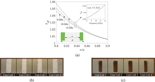
Figure 9. Frequency responses for prototypes (a) LIW composed of FR4 and foam, (b) WLIW machined of FR4.
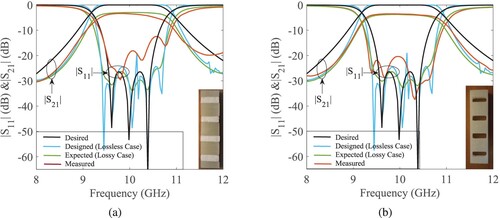
To avoid the aforementioned drawbacks of a LIW structure, WLIW is proposed and the designed prototype of WLIW is given in Figure (c). As in previous examples, EMT is utilized to determine the air-gap ratio w/a for the geometry of the WLIW design. The lateral width (i.e. ) and w/a of cavity parts are determined as 1.92 and 0.832 mm, respectively. The frequency response of the designed structure for which the losses are ignored is plotted together with the desired response in Figure (b) where similar proximity can be observed as in LIW design. On the other hand, the measurement results show the superiority of the proposed WLIW approach over the LIW design, which can be observed by comparing the measurement results with the design, including the losses of the substance. This improvement is mainly due to the mechanical stability of the designed geometry, thanks to the use of one single material.
The computational times are recorded in seconds around 25, 67, 393 through LIW and 26, 30, 453 through WLIW designs for Design 1, Design 2, and Prototype designs, respectively, with a standard PC. It is observed that the computational time increases for lower dielectric contrast in the unit cell and the use of a frequency-dependent dielectric material. Besides, the total sizes of designed filters are around or less than 10 cm in total as listed in Table . The proposed method promises effectiveness in terms of both computational time and physical compactness.
5. Discussion and conclusions
The classical design approaches, such as microwave filter theory or direct optimization methods, are inefficient for dielectric-loaded waveguides because these techniques highly likely produce a final solution with an arbitrarily varying dielectric profile, which cannot be practically obtained or manufactured. For practical and efficient solutions with pre-defined dielectric materials, a fast design procedure for dielectric-loaded waveguides is proposed. This procedure is formulated as an inverse problem, into which a non-linear optimization approach is integrated. Two types of dielectric configurations, an electrical discontinuity in longitudinal (LIW) or both widthwise and longitudinal (WLIW) directions, are considered. The design strategy is based on the dimensional optimization of the device by targeting the pre-defined scattering parameters. Since the desired frequency response is defined and targeted, the examined problem has to deal with the existence problem. Inherently, the frequency responses of the designed devices are not in perfect proximity but very good agreement with the targeted responses and are capable of satisfying the fundamental expectations of a filter such as bandwidth characteristics, passing and rejecting the signal in and out of the pass-band, respectively. The designer's experience becomes naturally a vital part of the design procedure because it is solved in the manner of an inverse design approach through an optimization procedure. For instance, the synthesis of filters is proposed to be designed by cascading multi-layered unit cells with high dielectric contrast in the unit cell, the sharpness of the filter increases with more unit cells or higher contrast can provide narrower bandwidth.
The main design procedure is the same for LIW and WLIW structures. To remedy the aforementioned potential drawbacks of a LIW structure, WLIW geometry is also proposed. The geometry of a WLIW is mapped to that of a LIW equivalence in terms of electrical properties by using effective dielectric permittivity and then the optimization procedure is carried out on the LIW equivalence having a frequency-dependent dielectric permittivity in the mapped parts. Regarding a compact structure (small in size) and ease of manufacturing (preparing the layers for LIW case and drilling the substance in WLIW case), a unit cell composed of a smaller number of layers is a favoured case. The resolution of the inverse problem (i.e. the number of layers in the unit-cell) can only be increased at the cost of high computation and the design of a bulky undesirable structure, but it is experienced that increased layers decrease the success of the proposed method. An examination of the number of unit cells is provided. Besides, designs are performed with different materials to show that different designs are possible. The numerical examples and measurement implementations provide successful results for both LIW and WLIW structures.
Acknowledgments
The authors would like to express their sincere thanks to Dr. Haluk Bayraktar and Mr. Ahmet Özkorucu for their help in manufacturing the device prototypes.
Disclosure statement
No potential conflict of interest was reported by the author(s).
Notes
1 An illustrative example is given in Appendix.
2 and
where
and
stand for real and imaginary part operators, respectively.
,
.
References
- Cameron RJ, Kudsia CM, Mansour RR. Microwave filters for communication systems, John Wiley and Sons, Inc.; 2018.
- Bui LQ, Ball D, Itoh T. Broad-band millimeter-wave e-plane bandpass filters (short papers). IEEE Trans Microw Theory Tech. 1984;32:1655–1658.
- Vahldieck R. Quasi-planar filters for millimeter-wave applications. IEEE Trans Microw Theory Tech. 1989;37:324–334.
- Craven GF, Mok CK. The design of evanescent mode waveguide bandpass filters for a prescribed insertion loss characteristic. IEEE Trans Microw Theory Tech. 1971;19:295–308.
- Bachiller C, Esteban H, Boria VE. CAD of evanescent mode waveguide filters with circular dielectric resonators. 2006 IEEE Antennas and Propagation Society International Symposium; 2006.
- Morro JV, Esteban González H, Bachiller C, et al. Automated design of complex waveguide filters for space systems: a case study. Int J RF and Microw Comput-Aided Eng. 2007;17:84–89.
- Aydoğan A. A hybrid MoM/MM method for fast analysis of e-plane dielectric loaded waveguides. AEU - Int J Electron Commun. 2019;100:9–15.
- Khalaj-Amirhosseini M. Microwave filters using waveguide filled by multi-layer dielectric. Prog Electromagn Res. 2006;66:105–110.
- Ghorbaninejad H, Khalaj-Amirhosseini M. Compact bandpass filters utilizing dielectric filled waveguides. Prog Electromagn Res B. 2008;7:105–115.
- Khalaj-Amirhosseini M. Wideband differential phase shifters using waveguides filled by inhomogeneous dielectrics. Prog Electromagn Res. 2009;2:1486–1489.
- Khalaj-Amirhosseini M, Ghorbaninezhad H. Microwave impedance matching using waveguides filled by inhomogeneous dielectrics. Int J RF Microw Comput-Aided Eng. 2009;19:69–74.
- Khalaj-amirhosseini M, Ghorbaninejad-foumani H. Waveguide bandpass filters utilizing only dielectric pieces. Prog Electromagn Res. 2010;4:553–557.
- George EMTJ, Matthaei Leo Young L. Microwave filters, impedance-matching networks, and coupling structures. Dedham (MA): Artech House; 1980.
- Cohn SB. Direct-coupled-resonator filters. Proc IRE. 1957;45:187–196.
- Şimşek S, Topuz E, Niver E. A novel design method for electromagnetic bandgap based waveguide filters with periodic dielectric loading. AEU – Int J Electron Commun. 2012;66:228–234.
- Arndt F, Bornemann J, Vahldieck R. Design of multisection impedance-matched dielectric-slab filled waveguide phase shifters. IEEE Trans Microw Theory Tech. 1984;32:34–39.
- Arndt F, Frye A, Wellnitz M, et al. Double dielectric-slab-filled waveguide phase shifter. IEEE Trans Microw Theory Tech. 1985;33:373–381.
- Aydoğan A, Akleman F, Yıldız S. Dielectric loaded waveguide filter design. 2016 International Symposium on Fundamentals of Electrical Engineering (ISFEE); 2016.
- Aydoğan A, Akleman F. An approximation for direct and inverse problems related to longitudinally inhomogeneous waveguides. 2016 International Symposium on Fundamentals of Electrical Engineering (ISFEE); 2016.
- Coleman TF, Li Y. An interior trust region approach for nonlinear minimization subject to bounds. SIAM J Optim. 1996;6:418–445.
- Branch MA, Coleman TF, Li Y. A subspace, interior, and conjugate gradient method for large-scale bound-constrained minimization problems. SIAM J Sci Comput. 1999;21:1–23.
- Shestopalov Y, Smirnov Y. Determination of permittivity of an inhomogeneous dielectric body in a waveguide. Inverse Probl. 2011;27:095010.
- Shestopalov Y, Smirnov Y. Numerical-analytical methods for the analysis of forward and inverse scattering by dielectric bodies in waveguides. 2012 19th International Conference on Microwaves, Radar & Wireless Communications; 2012.
- Shestopalov Y, Smirnov Y. Inverse scattering in guides. J Phys: Conf Ser. 2012;346: 012019.
- Smirnov YG, Shestopalov YV, Derevyanchuk ED. Inverse problem method for complex permittivity reconstruction of layered media in a rectangular waveguide. Phys Status Solidi (C) Current Top Solid State Phys. 2014;11:969–974.
- Chen J, Huang G. A direct imaging method for inverse electromagnetic scattering problem in rectangular waveguide. Commun Comput Phys. 2018;23:1415–1433.
- Smirnov YG, Medvedik MY, Moskaleva MA. Two-step method for permittivity determination of an inhomogeneous body placed in a rectangular waveguide. Lobachevskii J Math. 2018;39:1140–1147.
- Shestopalov Y. Justification of mathematical imaging technique for the permittivity determination of layered dielectrics in a waveguide. 2019 International Conference on Electromagnetics in Advanced Applications (ICEAA); 2019.
- Sheina EA, Shestopalov YV, Smirnov AP. Stability of least squares for the solution of an ill-posed inverse problem of reconstructing real value of the permittivity of a dielectric layer in a rectangular waveguide. 2019 PhotonIcs & Electromagnetics Research Symposium - Spring (PIERS-Spring); 2019.
- Sheina EA, Shestopalov YV, Smirnov AP. Advantages of a multi-frequency experiment for determining the dielectric constant of a layer in a rectangular waveguide and free space. Radio Sci. 2021;56: 1–4.
- Shestopalov Y. On unique solvability of multi-parameter waveguide inverse problems. 2017 International Conference on Electromagnetics in Advanced Applications (ICEAA); 2017.
- Mironov DA, Smirnov YG. On the existence and uniqueness of solutions of the inverse boundary value problem for determining the permittivity of materials. Comput Math Math Phys. 2010;50:1511–1521.
- Felici T, Engl HW. On shape optimization of optical waveguides using inverse problem techniques. Inverse Probl. 2001;17:1141–1162.
- Skaar J, Risvik KM. A genetic algorithm for the inverse problem in synthesis of fiber gratings. J Lightwave Technol. 1998;16:1928–1932.
- Minzioni P, Tormen M. Bragg gratings: impact of apodization lobes and design of a dispersionless optical filter. J Lightwave Technol. 2006;24:605–611.
- Kabir H, Zhang L, Yu M, et al. Smart modeling of microwave devices. IEEE Microw Mag. 2010;11:105–118.
- Norgren M. Chebyshev collocation and newton-type optimization methods for the inverse problem on nonuniform transmission lines. IEEE Trans Microw Theory Tech. 2005;53:1561–1568.
- Abazid MA, Lakhal A, Louis AK. Inverse design of anti-reflection coatings using the nonlinear approximate inverse. Inverse Probl Sci Eng. 2016;24:917–935.
- Amaya I, Correa R. Reconstructing design parameters of a rectangular resonator via peak signal-to-noise ratio and global optimization algorithms. Inverse Probl Sci Eng. 2017;25:864–886.
- Frickey DA. Conversions between S, Z, Y, h, ABCD, and T parameters which are valid for complex source and load impedances. IEEE Trans Microw Theory Tech. 1994;42:205–211.
- Khalaj-Amirhosseini M. Analysis of longitudinally inhomogeneous waveguides using the method of moment. Prog Electromagn Res. 2007;74:57–67.
- Chu TS, Itoh T. Generalized scattering matrix method for analysis of cascaded and offset microstrip step discontinuities. IEEE Trans Microw Theory Tech. 1986;34:280–284.
- Collin RE. Field theory of guided waves. 2nd ed. New York: Wiley-IEEE Press; 1991.
- Ansys HFSS Software. Available from: https://www.ansys.com/products/electronics/ansys-hfss.
- Aydoğan A, Akıncı MN, Akleman F. Complex permittivity determination only with reflection coefficient in partially filled waveguides. Meas Sci Technol. 2018;29:115601.
- Knott EF. Dielectric constant of plastic foams. IEEE Trans Antennas Propag. 1993;41:1167–1171.
Appendix.
Elements of  matrix
For the sake of readers' convenience, matrix Equation (Equation5(5)
(5) ) is explicitly expressed for N = 2 layers and M = 3 frequencies as
(A1)
(A1) where
,
,
,
,
,
. Let
, then
(A2)
(A2) Then, one can relate the elements of
and C matrices by element-wise division such as
,
,
,
and so on.