
Abstract
Homoepitaxial Si films have been deposited at a high rate of 200 nm s−1 over a wide area of 20 mm × 80 mm by cluster-assisted mesoplasma chemical vapor deposition (MPCVD) on a moving substrate. The obtained epitaxial Si films exhibited a uniform roughness of 0.1–0.3 nm (1 × 1 μm2) and a Hall mobility of ∼240 cm2 V−1 s−1. The results suggested that under the MPCVD the deposition precursors formed at the plasma edge could be small enough not to influence either epitaxial film structure or the film quality provided the substrate temperature is maintained above 500 °C.
1. Introduction
Single crystal Si thin films (scSiTF) are a potential solar cell material as the advantages of the stability and high conversion efficiency of single crystalline Si solar cells can be combined with low materials utilization in the form of thin films [Citation1]. To produce scSiTFs at an industry-compatible rate, ultrafast epitaxial deposition of Si films is required, combined with appropriate liftoff and layer transfer technologies [Citation2].
The well-adopted technique for the fast-rate Si epitaxy is thermal chemical vapor deposition and a deposition rate on the order of 10 nm s−1 is attained [Citation3, Citation4]. However, the production yield of Si from trichlorosilane (SiHCl3: TCS) is limited to 30% because this process is primarily based on the equilibrium chemistries. In contrast, mesoplasma chemical vapor deposition (MPCVD) can produce Si epitaxial films at a high rate of about 700 nm s−1 and a yield exceeding 50% from TCS. The high quality of MPCVD films resulted in a Hall mobility of about 70% of that of the p-type Si wafer [Citation5]. It is considered that the simultaneous attainment of these characteristics is attributed to its unique deposition process, which includes the formation of nanoclusters as deposition precursors and the high degree of non-equilibrium during epitaxial growth [Citation6]. When one considers the large area deposition with MPCVD, either plasma torch or substrate needs to be swept because the unique characteristics descried above are primarily attained by the plasma flow with inductively coupled plasma (ICP). In such an ICP geometry, spatial distribution of clusters [Citation7] and/or chemical species [Citation8], especially at the plasma flame edge, is in general believed to cause particle formation and thus alter the film structure and quality.
In this study, therefore, with an aim at a continuous deposition of epitaxial films at fast rates over a large area, we have attempted MPCVD by sweeping the substrate with a fixed plasma torch and identified the key factors that affect the large area Si epitaxy with a particular focus on the plasma edge effect.
Experimental details
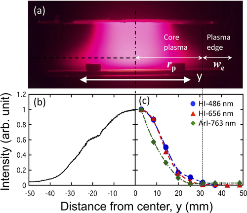
The MPCVD system used for the epitaxial Si film deposition is described elsewhere [Citation9, Citation10]. In this study, an X–Y–Z movable stage was introduced so that a large area deposition of Si films can be realized by sweeping the substrate. The plasma was generated inside a 40 mm diameter silicon nitride tube using a three-turn coil around a water-cooled quartz tube. An Ar/H2 mixture with a fixed flow rate of 21.6 L min−1 (Ar: 21 L min−1, H2: 0.6 L min−1) was used as a plasma gas. TCS was introduced as a source gas for the Si film deposition at a fixed flow rate of 50 sccm. The RF input power was fixed at 29 kW and the pressure of the chamber was fixed at 6 Torr throughout the experiments. Before deposition, the chamber was evacuated to a base pressure of less than 10−6 Torr. A typical optical image of the plasma flame taken by a digital camera during Si film deposition is shown in figure (a), together with the normalized spatial distributions of the intensity of the brightness of the plasma flame at the dashed line position (figure (b)) and also the normalized intensities of ArI and HI emissions after the Abel inversion analyzed from an optical emission spectroscopy (OES) observation (figure (c)). It is seen that the brightness of the plasma flame is weak already at a distance of 30 mm to the plasma center. It is also observed from the OES results that the light emissions are almost undetectable from a distance of 30 mm from the plasma center. Therefore, the core plasma that heats the substrate is defined as a circle area with a radius, r p , of 30 mm, and the plasma edge is defined as an annular area with a thickness of w e , as indicated in figure (a), in order to put a subsequent discussion in the context.
Figure 1 (a) A typical optical image of the plasma flame taken by a digital camera during Si film deposition, (b) a spatial distribution of the normalized intensity of the brightness of the plasma flame at the dashed line position, and (c) a spatial distribution of the normalized intensities of ArI and HI emissions after the Abel inversion analyzed from the OES results.
Single-crystal Si wafer with (100) orientation, 0.625 mm thick, and high resistivity (∼6000 Ω cm) was cut into and 20 mm × 80 mm (x × y) in sizes used as substrates. After being cleaned by ultrasonic rinsing with isopropanol and deionized water, it was placed on a water-cooled substrate holder. The substrate was moved in the y-direction, as shown in figure , with a scan range of 80 mm. The center of the substrate was moved from y = −40 to y = 40 mm. The position of y = 0 mm represented the center of the plasma flame. The deposition area was checked by the distribution of the film thickness and reasonably assumed to be the same as that of the plasma torch, i.e., a circle area with a diameter of 40 mm. The scan rates were varied from 0 to 20 mm s−1 and the deposition times (exposure time by the assumed deposition area with a diameter of 40 mm) were adjusted to maintain the film thicknesses at about 15 μm by changing the number of the scan. The maximum scan rate of 20 mm s−1 is limited by the system setup. The scan rate of 0 mm s−1 represented the stationary condition where the substrate was set in the center of plasma flame. Before deposition, the substrate was exposed by Ar/H2 plasma to remove the SiO2 layer on the surface and also to heat up the substrate. A boron nitride (BN) skirt was set at the torch exit and used for boron doping by exposure of the BN skirt to the periphery of the plasma flame. The distance between the substrate surface and skirt exit was fixed at 20 mm.
The surface and cross-sectional morphologies were observed by field-emission scanning electron microscopy (FE-SEM, Hitachi S-4200). The phases present in the films were analyzed by x-ray diffraction (XRD, M18XHF-SRA). The surface roughness was measured by atomic force microscopy using a scanning probe microscope (SPM-9700). Tapping-mode measurements were performed in air within a scan area of 1 × 1 μm2. The electrical properties of the films were measured by Hall effect measurements (Resitest 8300) at room temperature.
Results
The deposition rates of the Si films were calculated on substrates through the film thickness at the sample’s center and the exposure time by the assumed deposition area with a diameter of 40 mm. The variation of the deposition rate with the scanning half period (the time needed for the sample to return to the plasma center, ts = 80/v, see the inset in figure ), corresponding to the different scan rates (v), is shown in figure . It is seen that the deposition rate does not vary with the scanning half period/scan rate and is maintained at about 200 nm s−1. However, a change of the film structure is observed by varying the scan rate, which can be evidenced from the XRD patterns of the films measured at a
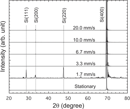
area of the sample’s center, as shown in figure . When the scanning half period is less than 25 s, i.e., the stationary condition and the conditions with a scan rate of higher than 3.33 mm s−1, the XRD patterns of the films show only Si (n00) peaks. The film that has such a XRD pattern has already been confirmed to be the epitaxial film in our former study by transmission electron microscopy observation [Citation11]. Therefore, the films obtained at these conditions are believed to be epitaxial films (single crystal Si films in this study). When the scanning half period increased to be ∼47 s, corresponding to the scan rate is decreased to 1.67 mm s−1, in addition to the strongest Si(400) peak from the film, peaks corresponding to (111) and (220) are observed, indicating the polycrystalline nature of the film.
Figure 2 Variation of the deposition rate of the films with the scanning half period at different scan rates deposited on 20 mm × 20 mm substrates. Inset: illustrative diagram for the scanning half period, v: scan rate.
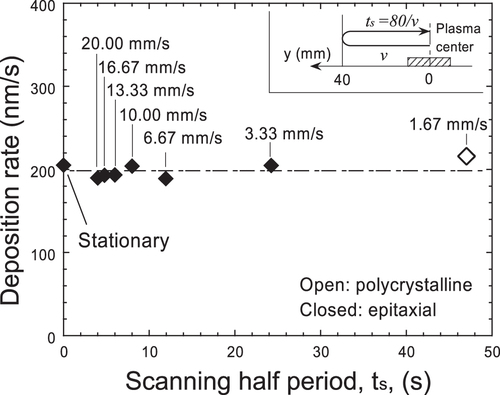
Figure 3 XRD patterns of the films deposited at different scan rates, measured at a 5 mm × 5 mm area of the center of the 20 mm × 20 mm substrates.
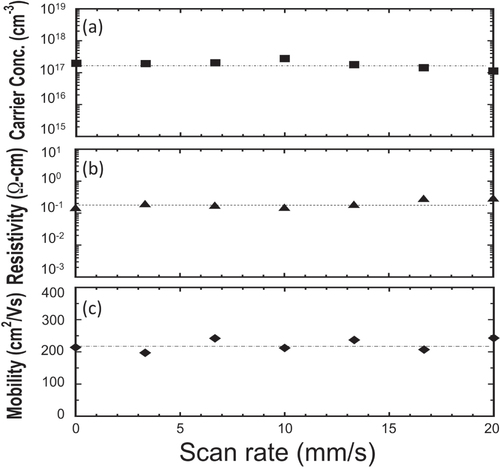
The electrical properties of the epitaxial Si films (single crystal Si films) measured at the center of samples are shown in figure . All of these films are confirmed to be the p-type Si due to the boron doping and the effect of boron doped into substrate on the film properties is confirmed to be negligible from the measured constant resistivity of the films at different thicknesses (results are not shown here). It is seen that the electrical properties of the epitaxial Si films are not affected by the scan rate. The carrier concentration has an average value of about 2.0 × 1017 cm−3, the average resistivity of the films is about 0.2 Ω cm, and the Hall mobility of the films is about 220 cm2 V−1 s−1 on average, which is about 70% of that of the p-type commercial Si wafer [Citation12].
Figure 4 Scan rate dependences of the (a) carrier concentration, (b) resistivity, and (c) Hall mobility of the epitaxial Si films at the center of the samples (20 mm × 20 mm substrate).
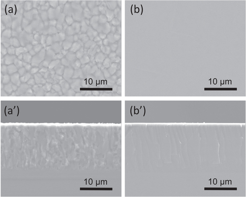
The film structure is not only varied with the scan rate, but also varied with the position. Figure shows the images of the samples with a size of 20 mm × 80 mm (x × y) obtained by sweeping the substrate along the y-direction with scan rates of 3–20 mm s−1. The samples are symmetrical in the y-direction versus the origin of the scale bar; therefore, only their halves are shown in the figure. There are two distinct regions colored white and black. Figure shows typical surface and cross-sectional SEM images of these two regions, revealing that the white region contains clear grain boundaries and the interface between the film and substrate, whereas the black region has a uniform structure with no clear interface (the residual structure results from the cleavage procedure). Actually, the films at the white region have been confirmed to be the polycrystalline films and those at the black region are epitaxial films. It is seen from figure that the width of the epitaxial film region from the sample’s center, l, is about 3 mm at the scan rate of 3 mm s−1. This epitaxial region increases with increasing scan rate and the epitaxial Si films on an area of 20 mm × 80 mm are obtained when the scan rate reaches
or higher.
Figure 5 Images of the samples deposited at different scan rates (half parts of the symmetrical samples on 20 mm × 80 mm substrates).
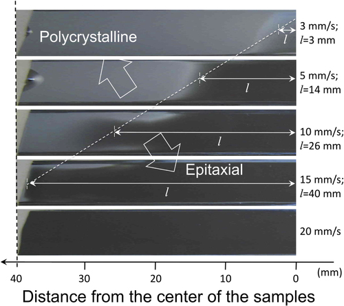
Figure 6 Typical surface (a), (b) and cross-sectional (a′), (b′) SEM images of the films at the white (a), (a′) and black (b), (b′) color regions shown in figure .
The epitaxial Si film obtained on 20 mm × 80 mm substrate at a scan rate of 20 mm s−1 has a mirror-like surface and is illustrated in figure . The Hall mobility and surface roughness (root mean square roughness (rms)) of this epitaxial Si film at the central positions along y-direction are shown in figures (a) and (b). It is seen that the Hall mobility of the films does not vary with position and has an average value of ∼240 cm2 V−1 s−1. The rms measured over a 1 × 1 μm2 area is also not influenced by position and is determined to be in the range of 0.1–0.3 nm with an average value of ∼0.2 nm. The film thicknesses are also measured by a surface profiler and show a deviation of < ± 5% along the y-direction. Therefore, a large area deposition of epitaxial Si films can be realized by MPCVD through a sweeping of the substrate and the epitaxial Si films show good uniformities of the surface roughness and electrical properties.
Figure 7 Position dependences of the (a) Hall mobility, (b) surface roughness (rms), and (c) ratio of the plasma core/edge exposure time [τ p/τ e] normalized to their maximum value for the epitaxial Si film deposited at a scan rate of 20 mm s−1.

Discussion
In order to indentify the so-call ‘edge effect’, i.e., particles are formed at the plasma edge and incorporated into the film disrupting the epitaxial growth, on the epitaxial Si film deposition in MPCVD, it is necessary to identify the core and edge plasma regions. It has been mentioned in the experimental section that the core plasma is defined as a circle region with a radius of 30 mm. When the substrate with
in size sweeps repeatedly under the plasma with a range of 80 mm, it is inevitably exposed to both the core plasma and plasma edge. Since the plasma condition is fixed, the fluxes of the deposition precursors to the substrate from the core plasma and plasma edge regions are constant. Therefore, the degree of the ‘edge effect’ can be quantitatively expressed by the ratio of the exposure time of the core plasma (τ
p) to that of the plasma edge (τ
e), i.e., τ
p/τ
e. When the τ
p/τ
e ratio is low, the ‘edge effect’ is more significant, favoring the formation of polycrystalline films.
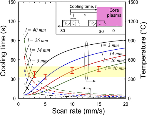
The τ p/τ e ratio only depends on the radius of the core plasma, the thickness of the plasma edge, and also the range of sweeping. It is independent of the scan rate. Therefore, the variations of the τ p/τ e ratio with position are the same for all of the films deposited at different scan rates. Because it is impossible to identify the region of the plasma edge correctly, the thickness of the plasma edge, w e , is selected to be 10 mm, 20 mm, 30 mm, 40 mm, and infinity, respectively, to only demonstrate the variation of the τ p/τ e ratio with position. Figure (c) shows the τ p/τ e ratios of the substrate at different positions at one full scan (the center of the substrate is swept from y = −40 to 40 mm) normalized to their maximum values. It is seen from the figure that the τ p/τ e ratio at sample’s center is smaller than that at the position of 10 mm from center when w e is defined as 10 mm. When w e is defined to be 20 mm or thicker, the τ p/τ e ratio at the central region (from −10 to 10 mm) is much larger than that at the edge region and the τ p/τ e ratio at the edge region decreases with increasing w e . For the conventional flame type plasma, these differences in the τ p/τ e ratio at different positions inevitably affect the film structure and also its properties if the so-call ‘edge effect’ exists. However, under the mesoplasma condition, the structure and quality of the film deposited at the scan rate of 20 mm s−1 (figure ) are independent of τ p/τ e ratio. Therefore, it is suggested that the epitaxial Si film deposition under MPCVD can be free from the so-called ‘edge effect’.
However, even if the plasma condition is unchanged at different scan rates, formation of polycrystalline film at the edge of the substrate is observed when the scan rate is slower than 15 mm s−1. The region of such polycrystalline film increases with decreasing scan rate, as shown in figure . In the MPCVD process, the substrate is heated only by plasma exposure. Therefore, its temperature at certain position decreases as it is swept out of the core plasma region. Once it returns to the edge of the core plasma, it is heated up and its temperature rises. Therefore, the minimum substrate temperature during sweeping depends on the cooling time before the substrate reaches the edge of the core plasma. Since the scan ranges for all of these experiments are constant, for the certain position of the substrate, the faster the scan rate, the less the cooling time, thus the higher the substrate temperature. Therefore, the formation of polycrystalline film and the change of its region in this study could be related to the substrate temperature.
Figure shows the temperature profile of the substrate (red line) with cooling time, t, measured at the center of the substrate (y = 0 mm) at the stationary condition by an infrared thermocouple after the plasma power turned off. This temperature profile can be well fitted by a lumped capacitance model, which is expressed as,(1)
where T
w
is the cooling water temperature (K), T
0 initial substrate temperature (K), S substrate area (m2), h heat transfer coefficient (W m-2 K), ρ density of Si (g cm−3), C specific heat of Si (J g−1 K), and V substrate volume (m3). Here, the heat transfer coefficient, h, is estimated to be 278 W m−2 K. This good agreement of the temperature profiles suggests that the substrate temperature is primarily controlled by the vertical heat transfer and the lateral heat conduction can be fundamentally ignored. Therefore, when moving the substrate, any position of the substrate is heated within the plasma flame and is immediately cooled down once it moves out of the core plasma region. The cooling duration and the minimum temperature after cooling at any position can thus be estimated by the scan rate, scan range, and the radius of the plasma core, using equation (Equation1
(1) ).
Figure 8 Measured temperature profile of the substrate at center of the substrate after the plasma turned off and its fitted curve with a lumped capacitance model.
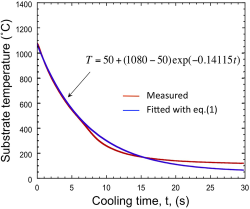
Figure shows the estimated cooling time (the cooling duration before it reaches the core plasma edge) and minimum substrate temperature at the epitaxial-polycrystalline structure transition region shown in figure as a function of scan rate. It is seen that the minimum substrate temperature at the structure transition regions is in the range of 350–550 °C despite different scan rates. In other words, epitaxial Si film is deposited as long as the substrate temperature is maintained higher than this critical temperature. Therefore, the minimum substrate temperature is critically influential to the film structural formation and the deposition precursor formed at the plasma edge is not necessarily obstructive for the Si epitaxial growth.
Figure 9 Estimated scan rate dependences of the cooling time and minimum temperature for the substrate at the structure transition region shown in figure . Inset: illustrative diagram of the cooling procedure of the substrate at the structure transition region. (P: polycrystalline; E: epitaxial; υ: scan speed. Dotted line: center of the sample).
According to the molecular dynamics (MD) simulation of the cluster impingement on the substrate during epitaxial growth, there seems a minimum substrate temperature at which the loosely bound nanoclusters exhibit instantaneous and spontaneous cluster deformation and atomic rearrangement for the fast rate epitaxy [Citation13] even in the plasma core. At the plasma edge, in contrast, rigid particles with the same size are expected to form. Assuming that the rigid particle with a size as small as 2 nm is created, the melting point of such a particle is estimated to be 540 °C considering the
curvature effect using the data in [Citation14]. This temperature is close to the estimated critical temperature for the structure transition in this study. This is suggestive that even if the rigid particles are formed at the plasma edge, they are potentially melt on the substrate surface and contribute to the epitaxial growth as long as the size is that small. Furthermore, the MD simulation also has suggested that if the loosely bound cluster is as large as around 5 nm, the comprising Si atoms are not fully rearranged for epitaxy even at a high substrate temperature [Citation15]. However, there is a fact that wide area epitaxy is attained at the faster scan rate of 20 mm s−1, incorporating the clusters/particles from the plasma edge. Therefore, the deposition precursors at the plasma edge could be small and do not critically affect the epitaxial growth as long as the substrate temperature is high enough. This may be one of the characteristics of the MPCVD and is advantageous for large area Si epitaxy.
Conclusions
Using MPCVD, epitaxial Si films have been deposited at 200 nm s−1 on a wide area of 20 mm × 80 mm by sweeping the substrate at a scan rate of 15 mm s−1 or higher. The films have exhibited reasonable uniformities of the surface roughness of 0.1–0.3 nm (1 × 1 μm2) and Hall mobility of
The deposition precursors formed at the plasma edge were small even under the intermediate pressure mesoplasma condition and the epitaxial Si film deposition by MPCVD can be free from the ‘edge effect’ provided the substrate temperature is maintained above ∼500 °C. Therefore, wide-area epitaxial deposition should be possible by aligning several ICP torches together in row, thereby eliminating the ‘edge effect’.
Acknowledgement
This work was partly supported by Grant-in-Aid for Scientific Research (S) 21226017 from the Ministry of Education, Culture, Sports, Science and Technology of Japan (MEXT).
References
- ReberSHurrleAEyerAWillekeG 2004 Sol. Energy 77 865 875 865–75 10.1016/j.solener.2004.08.021
- BeaucarneGDuerinckxFKuzmaIVan NieuwenhuysenKKimH JPoortmansJ 2006 Thin Solid Films 511-512 533 542 533–42 10.1016/j.tsf.2005.12.003
- GordonIVallonSMayoletABeaucarneGPoortmansJ 2010 Sol. Energy Mater. Sol. Cells 94 381 385 381–5 10.1016/j.solmat.2009.08.015
- HabukaHAoyamaYAkiyamaSOtsukaTQuW FShimadaMOkuyamaK 1999 J. Cryst. Growth 207 77 86 77–86 10.1016/S0022-0248(99)00360-7
- WuSKambaraMYoshidaT 2013 Plasma Chem. Plasma Process. 33 433 451 433–51 10.1007/s11090-013-9439-7
- DiazJ M AKambaraMYoshidaT 2008 J. Appl. Phys. 104 013536 10.1063/1.2956692
- HanPYoshidaT 2002 J. Appl. Phys. 92 4772 4778 4772–8 10.1063/1.1506396
- RennickC JEngelnRSmithJ AOrr-EwingA JAshfoldM N RMankelevichY A 2005 J. Appl. Phys. 97 113306 10.1063/1.1906288
- SawayanagiMDiazJ M AKambaraMYoshidaT 2007 Surf. Coat. Technol. 201 5592 5595 5592–5 10.1016/j.surfcoat.2006.07.134
- ChaeY KOhnoHEguchiKYoshidaT 2001 J. Appl. Phys. 89 8311 8315 8311–5 10.1063/1.1370365
- FukudaJKambaraMYoshidaT 2011 Thin Solid Films 519 6759 6762 6759–62 10.1016/j.tsf.2011.01.216
- SzeS MNg KwokK 1981 Physics of Semiconductor Devices 3rd edn New York Wiley 29
- ChenL WShibutaYKambaraMYoshidaT 2013 Chem. Phys. Lett. 564 47 53 47–53 10.1016/j.cplett.2013.02.005
- The Japan Institute of Metals and Materials 1993 Kinzoku Data Book 3rd edn Japan Maruzen 11 16 11–6
- ChenL WShibutaYKambaraMYoshidaT 2012 J. Appl. Phys. 111 123301 10.1063/1.4729057