
 ?Mathematical formulae have been encoded as MathML and are displayed in this HTML version using MathJax in order to improve their display. Uncheck the box to turn MathJax off. This feature requires Javascript. Click on a formula to zoom.
Abstract
Transition metal diboride thin films are promising functional materials for their outstanding mechanical properties and thermal stability. By combining experiment and simulations, we discuss angular distribution of the sputtered species, their scattering in the gas phase, re-sputtering and potential evaporation from the grown films for the complex evolution of film compositions, as well as energetic preference for vacancy formation and competing phases as factors for governing the phase constitution. By co-sputtering from two compound targets, we developed phase-pure crystalline (Ta,Al)B2 solid solution thin films and correlate the stoichiometry changes with the evolution of their microstructure, hardness, and elastic modulus.
GRAPHICAL ABSTRACT

Transition metal diborides (TMB2) combine outstanding chemical stability, high hardness, and good thermal conductivity, providing a suitable basis for high-temperature applications [Citation1–3]. TMB2 crystalize in two types of hexagonal structures, α-AlB2 (space group 191-P6/mmm) and ω-W2B5-x (space group 194-P63/mmm), referred to as α and ω [Citation1,Citation2]. Early TMB2 (TiB2 [Citation4], VB2 [Citation5], ZrB2 [Citation6], NbB2 [Citation7], HfB2 [Citation8], TaB2 [Citation9]) energetically tend to crystalize in the α structure, while late TMB2 (MoB2 [Citation10], WB2 [Citation11], etc.) favor the ω structure. Nevertheless, phase preference can change in the presence of point defects (mainly vacancies [Citation1,Citation12,Citation13]).
Binary TMB2, however, are typically brittle and have unfavorable oxidation resistance. A strategy to improve these properties is Al-alloying, shown promising for Ti-Al-B [Citation14–16], Re-Al-B [Citation17], and Ta-Al-B [Citation18]. Here, we focus on (Ta1-xAlx)By as a model system, which currently has no Ta-Al-B phase diagram available. The parent TaB2 was recently prepared by direct current (DC) magnetron sputtering [Citation19], pulsed direct current magnetron sputtering [Citation9], radio frequency (rf) magnetron sputtering [Citation20] using a TaB2 target, and by DC magnetron sputtering using a TaB4 target [Citation21]. TaB2 showed high hardness of 45.9 GPa with (0001) preferred orientations [Citation21] and provided theoretical basis for ductility [Citation1,Citation22,Citation23]. Šroba et al. [Citation18] synthesized over-stoichiometric Ta0.75Al0.25B2.14 and Ta0.69Al0.31B2.16 thin films by magnetron co-sputtering, with reference to sub-stoichiometric TaB1.21 thin film. The Ta0.75Al0.25B2.14 and Ta0.69Al0.31B2.16 thin films revealed a nanocomposite structure consisting of α-TaB2 nanofilaments surrounded by Al-rich tissue phase.
Development of stoichiometric magnetron-sputtered TMB2 thin films is challenging, since their composition typically deviates from 1:2 metal-to-boron stoichiometry (e.g. TiB2.72, HfB2.36, CrB2.27, WB1.88, and TaB1.53 [Citation24]). For one of the most widely studied diborides, TiB2, Neidhardt et al. [Citation25] showed that the B over-stoichiometry can be attributed to preferential emission of light B atoms (10.8 amu) along the target normal (0°) and sputtering of the relatively heavier Ti atoms (47.9 amu) under larger angles with respect to the target normal. Additionally, the authors demonstrated that B over-stoichiometry can be mitigated at higher Ar deposition pressures or larger target-to-substrate distances, i.e. by more scattering of B and Ti on Ar. Furthermore, Petrov [Citation26] and Hellgren [Citation27] pointed towards the ionization degree of the sputtered species as another important factor. The sputtered Ti atoms were selectively ionized due to their relatively lower ionization potential compared to B. Thereby, the B/Ti ratio could be controlled to synthesize stoichiometric TiB2 films [Citation26]. With an external magnetic field, the Ti ions were steered toward films. Hellgren et al. [Citation27] revealed lower B/Ti ratios of TiBx thin films deposited from high-power impulse magnetron sputtering (HiPIMS, with higher ionization degree) compared with those from direct current magnetron sputtering (DCMS) deposition, as Ti is ionized at a higher rate than B due to its lower ionization potential and higher ionization cross-section. Recently, Glechner et al. [Citation24] suspected the mass difference and scattering effects can also explain formation of over-stoichiometric CrB2.27 since Cr (52.0 amu) has similar mass as Ti. Contrary, sputtering the TaB2 and W2B5 targets ended up with sub-stoichiometric TaB1.53 and WB1.88 thin films. Šroba et al. [Citation9] synthesized TaBx films ranging from TaB3.84 to TaB1.36. They ascribed the decreasing boron content with increasing acceleration voltage to the more pronounced boron re-sputtering with an increase of the energy of backscattered Ar neutrals.
In addition to the film composition, the phase constitution is governed by the thermodynamics (including vacancy formation energies) and kinetics [Citation9,Citation12,Citation28], which, however, requires further evidence.
Here we develop solid solution (Ta1-xAlx)By thin films with different B and Al stoichiometry and show how it relates to the films’ microstructure and mechanical properties. The effects of sputtering, scattering, re-sputtering, based on the previous work in Refs. [Citation25–27] and Ref [Citation9], potential evaporation, formation energies of vacancies and competing phases as well as evolution of the film microstructure and mechanical properties are discussed.
The films were prepared from 2” TaB2 and AlB2 targets (Plansee Composite Materials GmbH) by a lab-scale magnetron sputtering system (AJA Orion 5). The targets were DC sputtered with power control, using AlB2/TaB2 power ratios (abbreviated Al/Ta-PR) of 0.0 (0 W/200 W), 0.5 (100 W/200 W), 1.0 (200 W/200 W), 2.0 (200 W/100 W) and 4.0 (200 W/50 W). Inductively coupled plasma mass spectrometry (ICP-MS) analysis showed target compositions of AlB1.96 and TaB2.35, respectively. The measured Ta-B target composition is different from the perfect stoichiometric one specified by Sroba et al. [Citation9], revealing that manufacturing is not simple and the resulting variations in the B content may to some extent influence the deposition.
Single crystal Si (100) and sapphire (102) substrates were ultrasonically cleaned with acetone and ethanol. After mounting these to the rotatable substrate holder—being confocal to the targets and 7 cm above them—the chamber was evacuated to a base pressure below 6 × 10⁻⁴ Pa. After reaching ∼450 ℃, the substrates were Ar-ion etched for 10 min with a DC bias of −750 V and 6 Pa Ar. The depositions were performed with a substrate temperature of ∼450 ℃, an Ar pressure of 0.4 Pa, and a substrate bias of −40 V DC.
Compositions of films on sapphire substrates were determined by inductively coupled plasma optical emission spectroscopy (ICP-OES), accurate for both B and metals [Citation29,Citation30]. Target sputtering and film (re-)sputtering were modeled by dynamic stopping and range of ions in matter (TRIDYN) simulations [Citation31], assuming 5 × 10⁵ Ar projectiles. In both cases, projectile incidence along the target or film normal (0°) was assumed. For sputtering, kinetic energies of Ar+ ion corresponding to the target potentials of the prepared films were chosen (Suppl. Tab, S1). Re-sputtering from stoichiometric TaB2 films was roughly simulated with the maximum kinetic energy of backscattered Ar atoms obtained from (Equation (1) [Citation32]), which is dependent on the TaB2 target potentials. Re-sputtering from compound (Ta1-xAlx)B2 films was simulated with Ar energy of 193 eV (the maximum Ar kinetic energy corresponding to TaB2 target potential of 480 V). Structural characterization was conducted by X-ray diffraction (XRD, PANalytical XPert Pro MPD) with a Cu-Kα source (wavelength λ = 1.5408 Å) at 45 kV and 40 mA in Bragg Brentano mode. The morphologies of films on Si substrates were investigated by a field emission scanning electron microscope (FE-SEM, Zeiss Sigma 500 VP). Transmission electron microscope (TEM) investigations were conducted using an FEI Tecnai F20 operated at 200 kV. The sample was prepared by a standard lift-out procedure using a ThermoFisher Scios 2 dual-beam focused ion beam (FIB) system. Indentation hardness (H) and Young’s modulus (E) were assessed from films on Si substrates by nanoindentation (Ultra Micro Indentation System, UMIS) with a Berkovich diamond tip following the Oliver and Pharr method [Citation33]. On every sample, 30 indents with loads from 3 to 30 mN were conducted, and their load-displacement curves were analyzed assuming a Poisson’s ratio of 0.25 (based on our calculations—described below—and Ref. [Citation18]). The reduced moduli were converted into the Young’s moduli by the Equation (2) in [Citation34].
To understand the phase constitution, Density Functional Theory (DFT) calculations were performed employing the Vienna Ab initio Simulation Package (VASP) [Citation35–37] with the Perdew–Burke–Ernzerhof functional [Citation38] for approximating the exchange–correlation effects and the projector augmented plane wave (PAW) method. From the equilibrated structure of hexagonal α-TaB2 (P6mmm) and orthorhombic o-TaB (Cmcm), we built a 108-atom (3 × 2 × 3) and a 128-atom (4 × 1 × 4) supercell with the PHONOPY package [Citation38], as a model of α-(Ta1−xAlx)B2-z and o-(Ta1−xAlx)B solid solution, respectively. Al atoms and B vacancies were distributed on the metal and B sublattice, respectively, according to the Special Quasirandom Structure (SQS) method [Citation39]. All structures were fully optimized (using a 7 × 6 × 6 and a 5 × 7 × 5 k-mesh of the Brillouin zone for the α- and o-phase, respectively, with a plane-wave cutoff energy of 600 eV) until forces on atoms not exceeding 10−5 eV/Å. Formation energy was calculated as.
where Etot is the total energy of the simulation cell, nTa (nAl, nB) number of Ta (Al, B) atoms, and μTa (μAl, μB) the corresponding chemical potential equal to the total energy per atom of the bcc-Ta (fcc-Al, and trigonal-B).
The growth rates are ∼6.7, 6.7, 9.0, 6.1 and 4.0 nm/min as Al/Ta-PR increases from 0.0 to 4.0. The initial increase corresponds to the additional powering of another sputter source, as the TaB2 target was always operated with 200 W for Al/Ta-PR of 0.0, 0.5, and 1.0. Subsequently, the deposition rate decreases as the TaB2 target power decreases.
The chemical composition analysis uses the ICP-OES method (Suppl. Table S1). Sole sputtering of the TaB2.35 target results in TaB1.23 films. With increasing the Al/Ta-PR from 0.5 to 4.0, both the Al/(Ta + Al) ratio (x) and the B/metal ratio (y) increase (Figure a), yielding films with compositions of (Ta0.997Al0.003)B1.64, (Ta0.95Al0.05)B2.0, (Ta0.80Al0.20)B2.3, and (Ta0.52Al0.48)B2.3, respectively.
Figure 1. (a) B/metal ratio (y, corresponding to axis on the left) indicated by red empty pentagons, and Al metal fraction (x, corresponding to axis on the right) indicated by black empty parallelograms, of the Ta1-xAlxBy films when using various AlB2/TaB2 target sputter power ratios (Al/Ta-PR); (b) XRD patterns of these films in their as-deposited state on sapphire substrates. The standard peak positions for the α-type h-TaB2 (ICDD 0038-1462, P6/mmm 191) and h-AlB2 (ICDD 0039-1483, P6/mmm 191) are indicated with filled and empty hexagons, respectively. The squared symbols mark the standard peak positions for o-TaB (0035-0815, Cmcm 63), and the asterisks indicate the positions of the substrate.
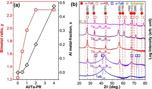
The factors controlling the film composition are the arrival and loss fluxes of film-forming species. The former depends on the sputter elements angular distribution functions from the target (ADF) and their scattering in the Ar atmosphere [Citation24,Citation25]. The TRIDYN simulations of the ADF of Ta, Al, and B from stoichiometric targets show ADF similar to Ti and B [Citation24], i.e. preferential sputtering of B along the target normal and sputtering of the Ta or Al under higher angles (data not shown). Sole consideration of the ADFs would suggest synthesis of B over-stoichiometric films [Citation24]. By considering of scattering of the sputtered species in Ar as the pressure or target-to-substrate distance is increased, synthesis of films with compositions approaching stoichiometry might be expected at p x d > 20 Pa cm [Citation15]. A pressure of 0.4 Pa and a target-to-substrate distance of 7 cm, p x d = 2.8 Pa cm, suggest limited impact of gas phase scattering on the overall film composition.
Recently, synthesis of B sub-stoichiometric TaBx films was attributed to B re-sputtering from the film by energetic Ar neutrals [Citation9]. Ar+ ions are neutralized and can be reflected by the collision with target constituents heavier than Ar [Citation32] (Ta) possessing here about 40% of the energy of Ar+ ions (Equation (1) in [Citation31]). The TRIDYN simulations (not shown) reveal that more than 21% of the Ar+ flux towards the target is backscattered. Furthermore, TRIDYN simulations show a higher sputtering yield (Y) and higher normalized sputtering yield (Yn) (defined as the ratio of Y and the content of the target constituent in the target) of B compared to Ta (Suppl. Tab. S2), represented by Y(B)/Y(Ti) > 2 and Yn(B)/Yn(Ti) > 1, respectively, indicating preferential sputtering of B. In combination of both, the substantial flux of energetic backscattered Ar neutrals and the preferential sputtering of B can qualitatively explain B reduction in the growing film, resulting in B sub-stoichiometric films as observed experimentally.
The Y and Yn of the Ta, Al, and B based on similar TRIDYN simulations of re-sputtering of stoichiometric (Ta1-xAlx)B2 films are presented in Suppl. Tab. S3. Yn(B) and Yn(Al) show higher values than Yn(Ta), indicating their preferential re-sputtering over Ta, which leads to the formation of B- and Al-deficient films. Similar values of Yn(B) and Yn(Al) would suggest equal re-sputtering, i.e. equal reduction of their contents in the films, which, however, contradicts to a larger B and a small Al content in the films. The lower Al content in the films might potentially be caused, although not proven, by evaporation of the low melting point Al at the deposition temperature of 450°C. The impact of the different ionization degrees of Ta, Al, and B due to different ionization potentials and more efficient transport of their ions towards the substrate [Citation26,Citation40] on the film composition might be limited considering weakly ionized DC plasma without additional magnetic field utilized in this study.
XRD results (Figure b) indicate a dual-phase structure (α-TaB2 and o-TaB) for TaB1.23. The broad diffraction peaks at 2θ ∼ 41.0 and 67.3° suggest that the o-TaB phase is hugely strained and/or nanocrystalline, while the sharper peak at 2θ ∼ 27.6° indicates the presence of a coarser-grained α-TaB2 phase. Presence of B sub-stoichiometric phases instead of Ta segregation can be explained by energetically preferred formation of α-TaB1.75 with boron vacancies as well as o-TaB compared with stoichiometric α-TaB2, as suggested previously [Citation9] and also by our following DFT calculations. With increasing Al/Ta-PR from 0.0 to 0.5, the diffraction peak near 2θ ∼ 43° shifts closer to α-TaB2 and its intensity increases significantly. The reduced peak width suggests increased coherently diffracting domain sizes. These two findings agree well with the increased B/metal ratio of (Ta0.997Al0.003)B1.64. At first glance this might be in contrast to the grain-size reduction with increasing Al content observed by Hahn et al. [Citation11] for (W,Al)B2 solid solutions. However, the WB2 film was single-phased and the B content was between 60 and 65 at.% independent of the Al content. Unlike that, the Ta1-xAlxBy films yield an increasing B/metal ratio, y, from 1.23 to 2.29 and increased Al-metal fraction x, from 0.00 to 0.20 upon increasing Al/Ta-PR from 0.0 to 2.0, respectively. By increasing Al/Ta-PR to 4.0, for which y stays at 2.29, x increases to 0.48. Increasing Al/Ta-PR promotes the growth of the α-TaB2-based phase over o-TaB, which we relate to the higher B content and the higher Ef to form B vacancies (when Al is dissolved, see Ref. [Citation1]). The absence of AlB2 is likely the consequence of the close-to-zero Ef of α-AlB2 (−0.05 eV/at., from our following DFT calculations). As x increases to 0.48, the XRD peaks corresponding to the α phases gradually shift from the standard peaks of α-TaB2 towards those of AlB2, indicating the gradual solution of AlB2 into TaB2.
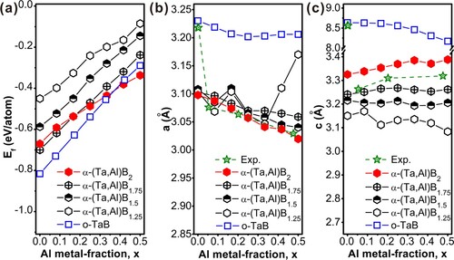
To rationalize phase constitution of our films and Al-induced changes in the B stoichiometry, we perform DFT calculations on energetic stability (estimated by formation energy, Ef, Figure a) and structural parameters (Figure b, c). Our ideal single-crystalline models consider the orthorhombic o-(Ta1−xAlx)B2 and the hexagonal α-(Ta1−xAlx)B2-z phase with x = 0–0.50 and z = 0–0.75. The o-TaB phase exhibits the most negative formation energy (Ef = −0.81 eV/at.), followed by α-TaB1.75 (i.e. α-TaB2 with B vacancies, Ef = −0.70 eV/at.) and the vacancy-free α-TaB2 (Ef = −0.67 eV/at.). Increasing the B vacancy content, the α phase becomes significantly less energetically favorable, as exemplified by α-TaB1.5 (Ef = −0.59 eV/at.) and α-TaB1.25 (Ef = −0.45 eV/at.). Consequently, the Al-free TaB1.23 film (prepared with Al/Ta-PR = 0) is unlikely a single-phase B-vacant α-TaB2 phase, however, more likely a mixture of o-TaB plus α-TaB2 or α-TaB1.75, as obtained experimentally. With increasing Al content, Ef of o-Ta1-xAlxB, α-Ta1-xAlxB2, and the B-vacant α-Ta1-xAlxB2-z become less negative (almost linearly), since α-AlB2 respectively o-AlB are significantly less stable than their Ta-counterparts. The vacancy-free α-Ta1-xAlxB2 provides the lowest slope with increasing Al content, suggesting that B-vacancies and the orthorhombic phase are less preferred with increasing Al content, as obtained by experiments. Already for x ∼0.16, vacancy-free α-(Ta1−xAlx)B2 becomes the preferred α-type phase over α-(Ta1−xAlx)B1.75. As α-(Ta1−xAlx)B2 and α-(Ta1−xAlx)B1.75 are energetically close (differing by maximum 0.03 eV/at. for x = 0), both may be accessible by PVD. Via later-presented STEM-EELS investigations of our films, we show evidence for the near-stoichiometric case. Lattice parameters, a and c, corresponding to all structures considered for Ef analysis are presented in Figure (b and c), respectively, depicting also experimental values based on XRD. The data in Figure (a) show that without Al, the o-TaB phase is dominant. For higher Al-contents, the experimental parameters follow nicely those of vacancy-free α-(Ta1−xAlx)B2 (hexagonal solid red marker).
Figure 2. (a) DFT calculated Ef of α-(Ta1−xAlx)B2-z solid solutions with various Al and B contents: x = 0–0.50 and z = 0–0.75. The corresponding lattice parameters a and c are depicted in (b) and (c), and directly compared to experimental values (dashed lines).
The phase constitution and composition with increasing B and Al contents strongly influence growth morphologies. The sub-stoichiometric TaB1.23 and (Ta0.997Al0.003)B1.64 films show a nearly featureless morphology of their fracture cross-sections, Figures (a and b), respectively. This agrees with their multiphase structure, where α-TaB2- and o-TaB-based phases compete during nucleation and growth. The nearly stoichiometric (Ta0.95Al0.05)B1.97, which is essentially single-phased α-(Ta,Al)B2, reveals a fine-fibrous growth morphology, because growth is not or only little hampered by another phase, Figure (c). This is even more pronounced for the (Ta0.80Al0.20)B2.29 film, presenting a dense columnar growth morphology, Figure (d). The highest Al-containing film, (Ta0.52Al0.48)B2.29, provides a somewhat fine growth morphology again, where the individual columns seem to be shorter as for (Ta0.80Al0.20)B2.29, compare Figure (d and e).
Figure 3. Upper row: SEM fracture cross sections of as-deposited Ta1-xAlxBy films on Si substrates. The Al content increases from (a) to (e): (a) TaB1.23, (b) (Ta0.997Al0.003)B1.64, (c) (Ta0.95Al0.05)B1.97, (d) (Ta0.80Al0.20)B2.29, and (e) (Ta0.52Al0.48)B2.29. Lower row: SEM surface morphologies of as-deposited Ta1-xAlxBy films on Si substrates. The Al content increases from (f) to (j): (f) TaB1.23, (g) (Ta0.997Al0.003)B1.64, (h) (Ta0.95Al0.05)B1.97, (i) (Ta0.80Al0.20)B2.29, and (j) (Ta0.52Al0.48)B2.29.
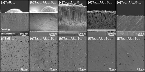
The domes visible at the surface of the fracture cross-sections, especially for TaB1.23, (Ta0.997Al0.003)B1.64, and (Ta0.95Al0.05)B1.97, are responsible for their rather rough surface and busy surface topography, see Figures (f–h), respectively. We envision that especially the competition of various phases causes this appearance. These will provide differences in adatom mobility and growth rates [Citation41]. The higher Al-containing films, (Ta0.80Al0.20)B2.29 and (Ta0.52Al0.48)B2.29, provide the smoothest surface and nicest SEM surface images, Figures (i and j), respectively.
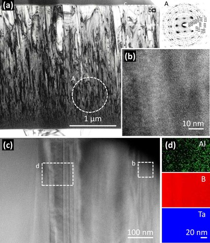
To further study the microstructure of Ta1-xAlxBy thin films, the nearly stoichiometric (Ta0.95Al0.05)B1.97 thin film was selected for TEM bright field (BF), selected area electron diffraction (SAED), high-angle annular dark field (STEM-HAADF) investigations, as depicted in Figure . The BF cross-sectional image (Figure a) shows a dense columnar structure. Directly at the interface with the substrate, the grains tend to be equiaxed and very small. They form elongated—initially V-shaped (which is typical for competitive growth)—columns, which initially have a small diameter, but then develop large diameters (approx. 500 nm) towards the thin film surface. The rather long columns, which become quite wide in the course of thin-film growth, suggest that there are no other phases that would interrupt their development. The SAED pattern from area A, which is near the interface and spans over several columns, shows a single-phase α-(Ta,Al)B2-based structure. The discrete diffraction spots are because the individual columns are nearly as long as the aperture size and the individual columns are highly oriented. The diffraction spots are nicely arranged along concentrical rings, which we calculated using the lattice parameters of a solid solution α-Ta1-xAlxB2 with a = 3.08 Å and c = 3.30 Å (see, Figures b and c for x ∼0.05). The high resolution TEM (HRTEM) image, Figure (b), reveals a nicely crystalline area with many lattice fringes. Within this image, which covers a region of ∼60 × 60 nm (marked in Figure a as well as Figure c), no grain boundaries or other phases (also no amorphous-like ones) can be identified. The rectangular region, labeled with c in Figure (a), was investigated by HAADF-STEM and exhibits only the columnar structure, Figure (c). The contrast variation essentially stems from thickness variations and difference between column interior (crystalline) and column boundaries. This is confirmed by EELS elemental mapping of an area that shows a higher density of these contrast variations (labeled with d in Figure c). Figure (d) shows that the distribution of Al, B, and Ta is homogeneous throughout this selected area (∼118 nm x 87 nm). The boron mapping indicates a bit of a columnar structure. Together with XRD (Figure b) and DFT (Figure ), these TEM investigations (BF, SAED, HRTEM, HAADF-SAED, EELS elemental mapping) clearly demonstrate the formation of a single-phase α-(Ta,Al)B2 solid solution thin film.
Figure 4. (a) TEM BF image with SAED of the circled area A on the right, (b) HRTEM image of the region indicated in (a) and (c), (c) STEM-HAADF image of a region indicated in (a), (d) EELS elemental mapping of Al, B, and Ta elements of the rectangular area indicated in (c) of the (Ta0.95Al0.05)B1.97 thin film grown on Si substrate. The lattice parameters of a = 3.08 Å and c = 3.30 Å are used to draw the circles of the SAED pattern.
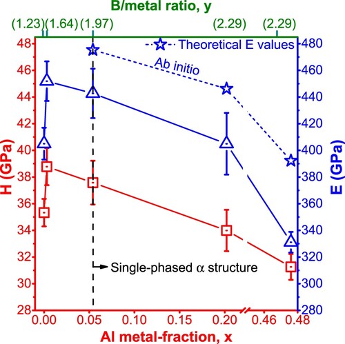
The chemical and structural variations cause variations in H and E, see Figure . The sub-stoichiometric TaB1.23 film, composed of α-TaB2 and o-TaB phases and with a nearly featureless growth morphology, yields H = 35.3 ± 1.0 GPa and E = 405.0 ± 11.9 GPa. Co-sputtering the AlB2 target with 100 W (Al/Ta-PR = 0.5)—which promotes the crystallization of the α-TaB2-based phase due to the noticeable increased B/metal ratio to y = 1.64 while still having only a rather small Al-metal fraction of x = 0.003 and a featureless growth morphology—leads to a (Ta0.997Al0.003)B1.64 film with highest H and E of 38.8 ± 1.4 and 451.9 ± 14.8 GPa, respectively. Further increasing Al/Ta-PR, which leads to nearly stoichiometric and even over-stoichiometric diboride films with increased Al-metal fractions, causes H and E to decrease with the Al content. Specifically, (Ta0.95Al0.05)B1.97, (Ta0.80Al0.20)B2.29, and (Ta0.52Al0.48)B2.29 yield H of 37.6 ± 1.6, 34.0 ± 1.6, and 31.3 ± 1.0 GPa, respectively. Also for W-Al-B and Ti-Al-B films the hardness decreases with increasing Al content [Citation42]. The decline in E with increasing Al content nicely follows the calculated variation based on a rule of mixture between the DFT value for α-TaB2 (E = 486 GPa) and α-AlB2 (E = 289 GPa), Figure . This suggests that the hardness reduction with increasing Al content mainly stems from changed binding characteristics. For these α-TaB2-phase dominated Ta1-xAlxBy films, variations in growth orientation, boron vacancies, and even a possible boron tissue phase—which all have their impact on hardness [Citation9,Citation43,Citation44]—are superimposed by the impact of Al.
Figure 5. Indentation hardness (H, corresponding to the left axis) indicated by red empty squares and Young’s modulus, (E, corresponding to the right axis) indicated by blue empty triangles, of as-deposited Ta1-xAlxBy films on Si substrates, with E values calculated from rule of mixture based on DFT polycrystalline E-moduli of α-TaB2 and α-AlB2 indicated by blue empty stars.
In conclusion, we established stoichiometry–microstructure–hardness relationships for novel single-phase α-structured (Ta,Al)B2 thin films. In addition to the preferential B emission along the target normal, Ta and Al emission at higher angles and limited gas phase scattering, the composition of the films is mainly governed by substantial re-sputtering of B and Al by energetic backscattered Ar neutrals and potential Al evaporation.
The thermodynamic stability without Al in the order o-TaB > B-vacant α-TaB1.75 > stoichiometric α-TaB2 is expected. Upon increasing x beyond ∼0.16 stoichiometric, α-Ta1-xAlxB2 is the most preferred among these α-phases.
In combination with the close-to-zero Ef of α-AlB2 and the preferred re-sputtering of Al, this explains why the increase of Al/Ta-PR to 0.5 leads to films with low B contents (y) at very low Al contents (x), such as Ta0.997Al0.003B1.64. This film is the hardest (H = 38.8 ± 1.4 GPa) among all Ta1-xAlxBy films studied. The Al/Ta-PR = 1.0 case allows for a nearly stoichiometric film having also a noticeable Al content, (Ta0.95Al0.05)B1.97, which is essentially single-phase α-structured with H = 37.6 ± 1.6 GPa and E = 451.9± 14.8 GPa. With a further increase in Al/Ta-PR to 2.0 and 4.0, the B content saturates at 2.29, while x continuously increases to 0.20 and 0.48, respectively. These films all reveal α-(Ta,Al)B2 as the dominant phase, however, with decreasing H and E following the x increase.
Our work showcases that explaining B non-stoichiometry of transition metal boride thin films requires considerations of sputtering of the target, re-sputtering of the growing film by energetic backscatter Ar neutrals reflected from heavy TM (compared with Ar) borides targets. Furthermore, except for film composition, the phase compositions can be correlated to defect formation energies and competing phases. Our findings provide a good basis for in-depth understanding of boride-based ceramic thin films and demonstrate the power of DFT and simulations in providing explanations and insights into new materials.
Supplemental Material
Download MS Word (25.1 KB)Acknowledgments
The authors highly appreciate discussions with Dr. R. Hahn from the Christian Doppler Laboratory for Surface Engineering of High-Performance Components, TU Wien, Austria.
Disclosure statement
No potential conflict of interest was reported by the author(s).
Additional information
Funding
References
- Moraes V, Riedl H, Fuger C, et al. Ab initio inspired design of ternary boride thin films. Sci Rep. 2018;8:9288. doi:10.1038/s41598-018-27426-w
- Euchner H, Mayrhofer PH. Designing thin film materials — ternary borides from first principles. Thin Solid Films. 2015;583:46–49. doi:10.1016/j.tsf.2015.03.035
- Magnuson M, Hultman L, Högberg H. Review of transition-metal diboride thin films. Vacuum. 2022;196:110567. doi:10.1016/j.vacuum.2021.110567
- Fuger C, Hahn R, Hirle A, et al. Revisiting the origins of super-hardness in TiB2+z thin films – impact of growth conditions and anisotropy. Surf Coat Technol. 2022;446:128806. doi:10.1016/j.surfcoat.2022.128806
- Cao Y, Li T, Xu Y, et al. Theoretical predictions of stability, electronic properties, elastic anisotropy, thermodynamics, and optical properties of MB2 (M = V, Nb, Zr). J. Mater. Sci. 2022;57:4605–4624. doi:10.1007/s10853-022-06898-2
- Yu H, Namini AS, Shakeri MS, et al. HRTEM study and mechanical properties of ZrB2–SiC composite: An insight into in-situ carbon formation over the SPS process. Int J Refract Met Hard Mater. 2022;104:105789. doi:10.1016/j.ijrmhm.2022.105789
- Nedfors N, Tengstrand O, Lu J, et al. Superhard NbB2− thin films deposited by dc magnetron sputtering. Surf Coat Technol. 2014;257:295–300. doi:10.1016/j.surfcoat.2014.07.087
- Nayak S, Singh CK, Dahlqvist M, et al. First-principles study on the superconductivity of doped zirconium diborides. Phys. Rev. Mater. 2022;6:044805. doi:10.1103/PhysRevMaterials.6.044805
- Šroba V, Fiantok T, Truchlý M, et al. Structure evolution and mechanical properties of hard tantalum diboride films. J Vac Sci Technol A. 2020;38:033408. doi:10.1116/6.0000155.
- Ding L-P, Shao P, Zhang F-H, et al. Crystal structures, stabilities, electronic properties, and hardness of mob2: first-principles calculations. Inorg. Chem. 2016;55:7033–7040. doi:10.1021/acsmorgchem.6b00899
- Hahn R, Moraes V, Limbeck A, et al. Electron-configuration stabilized (W. Al)B2 solid solutions. Acta Mater. 2019;174:398–405. doi:10.1016/j.actamat.2019.05.056
- Moraes V, Fuger C, Paneta V, et al. Substoichiometry and tantalum dependent thermal stability of α-structured W-Ta-B thin films. Scr Mater 2018;155:5–10. doi:10.1016/j.scriptamat.2018.06.005
- Dahlqvist M, Jansson U, Rosen J. Influence of boron vacancies on phase stability, bonding and structure of MB2 (M = Ti, Zr, Hf, V, Nb, Ta, Cr, Mo, W) with AlB2 type structure. J. Phys. Condens. Matter. 2015;27:435702. doi:10.1088/0953-8984/27/43/435702
- Bakhit B, Palisaitis J, Thörnberg J, et al. Improving the high-temperature oxidation resistance of TiB2 thin films by alloying with Al. Acta Mater. 2020;196:677–689. doi:10.1016/j.actamat.2020.07.025
- Navidi Kashani AH, Mráz S, Holzapfel DM, et al. Synthesis and oxidation behavior of Ti0.35Al0.65By (y = 1.7–2.4) coatings. Surf Coat Technol. 2022;442:128190. doi:10.1016/j.surfcoat.2022.128190
- Navidi Kashani AH, Hans M, Lellig S, et al. Morphology, mechanical properties, and oxidation behavior of stoichiometric Ti0.33-xAlxB0.67 coatings (x = 0.04, 0.15, 0.21, and 0.28). Acta Mater. 2024;270:119829. doi:10.1016/j.actamat.2024.119829
- Bliem P, Mráz S, Sen S, et al. Self-passivating (Re,Al)B2 coatings synthesized by magnetron sputtering. Sci Rep 2018;8:15570. doi:10.1038/s41598-018-34042-1
- Šroba V, Fiantok T, Truchlý M, et al. Structure evolution and mechanical properties of Al-alloyed tantalum diboride films prepared by magnetron sputtering co-deposition. J Vac Sci Technol A. 2023;41:023410. doi:10.1116/6.0002390
- Goncharov AA, Konovalov VA, Stupak VA. Effect of bias voltage on the structure of thin tantalum boride films. Tech Phys Lett. 2007;33:190–191. doi:10.1134/S1063785007030029
- Lin S-T, Lee C. Growth of tantalum boride films by RF magnetron sputtering effect of bias. J. Electrochem. Soc. 2003;150:G607–G611. doi:10.1149/1.1603253
- Liu C, Gu X, Zhang K, et al. Superhard metallic compound TaB2 via crystal orientation resolved strain stiffening. Phys. Rev. B. 2022;105:024105. doi:10.1103/PhysRevB.105.024105
- Pettifor DG. Theoretical predictions of structure and related properties of intermetallics. Mater Sci Technol. 1992;8:345–349. doi:10.1179/mst.1992.8.4.345
- Pugh SF. XCII. Relations between the elastic moduli and the plastic properties of polycrystalline pure metals. Lond. Edinb. Dubl. Phil. Mag. 1954;45:823–843. doi:10.1080/14786440808520496
- Glechner T, Oemer HG, Wojcik T, et al. Influence of Si on the oxidation behavior of TM-Si-B2 ± z coatings (TM = Ti, Cr, Hf. Ta, W). Surf. Coat. Technol. 2022;434:128178. doi:10.1016/j.surfcoat.2022.128178
- Neidhardt J, Mráz S, Schneider JM, et al. Experiment and simulation of the compositional evolution of Ti–B thin films deposited by sputtering of a compound target. J. Appl. Phys. 2008;104:063304. doi:10.1063/1.2978211
- Petrov I, Hall A, Mei AB, et al. Controlling the boron-to-titanium ratio in magnetron-sputter-deposited TiBx thin films. J Vac Sci Technol A. 2017;35:050601. doi:10.1116/1.4982649
- Hellgren N, Thörnberg J, Zhirkov I, et al. High-power impulse magnetron sputter deposition of TiBx thin films: Effects of pressure and growth temperature. Vacuum. 2019;169:108884. doi:10.1016/j.vacuum.2019.108884
- Dahlqvist M, Rosen J. Impact of vacancies on structure, stability and properties of hexagonal transition metal diborides, MB2 (M = Sc, Y, Ti, Zr, Hf, V, Nb, Ta, Cr, Mo, W, Mn, and Fe). Materialia. 2022;26:101629. doi:10.1016/j.mtla.2022.101629
- Cakara A, Bonta M, Riedl H, et al. Development of a multi-variate calibration approach for quantitative analysis of oxidation resistant Mo–Si–B coatings using laser ablation inductively coupled plasma mass spectrometry. Spectrochim Acta Part B. 2016;120:57–62. doi:10.1016/j.sab.2016.04.004
- Bahr A, Richter S, Hahn R, et al. Oxidation behaviour and mechanical properties of sputter-deposited TMSi2 coatings (TM = Mo, Ta, Nb). J. Alloys. Compd. 2023;931:167532. doi:10.1016/j.jallcom.2022.167532
- Ziegler JF, Ziegler MD, Biersack JP. SRIM – the stopping and range of ions in matter (2010). Nucl. Inst. Meth. Phys. Res. B. 2010;268:1818–1823. doi:10.1016/j.nimb.2010.02.091
- Chien Y-P, Mráz S, Fekete M, et al. Deviations between film and target compositions induced by backscattered Ar during sputtering from M2-Al-C (M = Cr, Zr, and Hf) composite targets. Surf. Coat. Technol. 2022;446:128764. doi:10.1016/j.surfcoat.2022.128764
- Oliver WC, Pharr GM. An improved technique for determining hardness and elastic modulus using load and displacement sensing indentation experiments. J. Mater. Res. 1992;7:1564–1583. doi:10.1557/JMR.1992.1564
- Fischer-Cripps AC. Critical review of analysis and interpretation of nanoindentation test data. Surf Coat Technol. 2006;200:4153–4165. doi:10.1016/j.surfcoat.2005.03.018
- Kresse G, Hafner J. Ab initio molecular dynamics for liquid metals. Phys. Rev. B. 1993;47:558–561. doi:10.1103/PhysRevB.47.558
- Kresse G, Furthmüller J. Efficiency of ab-initio total energy calculations for metals and semiconductors using a plane-wave basis set. Comput. Mater. Sci. 1996;6:15–50. doi:10.1016/0927-0256(96)00008-0
- Kresse G, Furthmüller J. Efficient iterative schemes for ab initio total-energy calculations using a plane-wave basis set. Phys. Rev. B. 1996;54:11169–11186. doi:10.1103/PhysRevB.54.11169
- Perdew JP, Ruzsinszky A, Csonka GI, et al. Restoring the density-gradient expansion for exchange in solids and surfaces. Phys. Rev. Lett. 2008;100:136406. doi:10.1103/PhysRevLett.100.136406
- Nöger D. A command line tool written in Python/Cython for finding optimized SQS structures, 13 (2019).
- Nedfors N, Primetzhofer D, Zhirkov I, et al. The influence of pressure and magnetic field on the deposition of epitaxial TiBx thin films from DC magnetron sputtering. Vacuum. 2020;177:109355. doi:10.1016/j.vacuum.2020.109355
- Delisle DA, Krzanowski JE. Surface morphology and texture of TiAlN/CrN multilayer coatings. Thin Solid Films. 2012;524:100–106. doi:10.1016/j.tsf.2012.09.073
- Ivanovskii AL. Hardness of hexagonal AlB2-like diborides of s, p and d metals from semi-empirical estimations. Int J Refract Met Hard Mater. 2013;36:179–182. doi:10.1016/j.ijrmhm.2012.08.013
- Fuger C, Hahn R, Zauner L, et al. Anisotropic super-hardness of hexagonal WB2 ± z thin films. Mater. Res. Lett. 2022;10:70–77. doi:10.1080/21663831.2021.2021308
- Mayrhofer PH, Mitterer C, Wen JG, et al. Self-organized nanocolumnar structure in superhard TiB2 thin films. Appl. Phys. Lett. 2005;86; doi:10.1063/1.1887824