Figures & data

Figure 1. (a) B/metal ratio (y, corresponding to axis on the left) indicated by red empty pentagons, and Al metal fraction (x, corresponding to axis on the right) indicated by black empty parallelograms, of the Ta1-xAlxBy films when using various AlB2/TaB2 target sputter power ratios (Al/Ta-PR); (b) XRD patterns of these films in their as-deposited state on sapphire substrates. The standard peak positions for the α-type h-TaB2 (ICDD 0038-1462, P6/mmm 191) and h-AlB2 (ICDD 0039-1483, P6/mmm 191) are indicated with filled and empty hexagons, respectively. The squared symbols mark the standard peak positions for o-TaB (0035-0815, Cmcm 63), and the asterisks indicate the positions of the substrate.
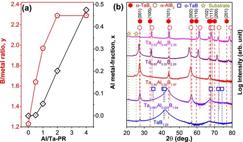
Figure 2. (a) DFT calculated Ef of α-(Ta1−xAlx)B2-z solid solutions with various Al and B contents: x = 0–0.50 and z = 0–0.75. The corresponding lattice parameters a and c are depicted in (b) and (c), and directly compared to experimental values (dashed lines).
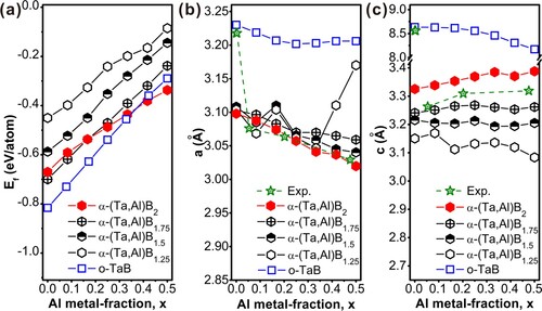
Figure 3. Upper row: SEM fracture cross sections of as-deposited Ta1-xAlxBy films on Si substrates. The Al content increases from (a) to (e): (a) TaB1.23, (b) (Ta0.997Al0.003)B1.64, (c) (Ta0.95Al0.05)B1.97, (d) (Ta0.80Al0.20)B2.29, and (e) (Ta0.52Al0.48)B2.29. Lower row: SEM surface morphologies of as-deposited Ta1-xAlxBy films on Si substrates. The Al content increases from (f) to (j): (f) TaB1.23, (g) (Ta0.997Al0.003)B1.64, (h) (Ta0.95Al0.05)B1.97, (i) (Ta0.80Al0.20)B2.29, and (j) (Ta0.52Al0.48)B2.29.
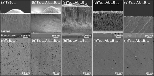
Figure 4. (a) TEM BF image with SAED of the circled area A on the right, (b) HRTEM image of the region indicated in (a) and (c), (c) STEM-HAADF image of a region indicated in (a), (d) EELS elemental mapping of Al, B, and Ta elements of the rectangular area indicated in (c) of the (Ta0.95Al0.05)B1.97 thin film grown on Si substrate. The lattice parameters of a = 3.08 Å and c = 3.30 Å are used to draw the circles of the SAED pattern.
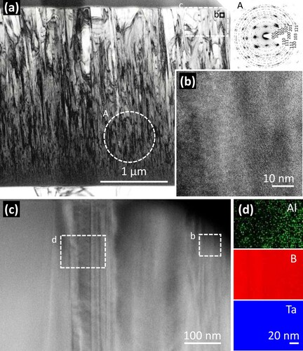
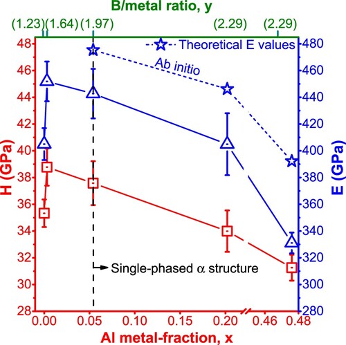
Figure 5. Indentation hardness (H, corresponding to the left axis) indicated by red empty squares and Young’s modulus, (E, corresponding to the right axis) indicated by blue empty triangles, of as-deposited Ta1-xAlxBy films on Si substrates, with E values calculated from rule of mixture based on DFT polycrystalline E-moduli of α-TaB2 and α-AlB2 indicated by blue empty stars.