
Abstract
Two-dimensional (2D) heterostructures have recently attracted interest as candidate materials for classical optoelectronics and in quantum information technology. Despite significant research, realizing deterministic, in-plane quantum confinement in synthetic 2D heterostructures at the nanoscale remains challenging. In this brief overview, we summarize recent advances in approaches for the growth of spatially controllable 2D quantum heterostructures. These growth methods enable the achievement of various 2D lateral/vertical heterostructures with controlled positions and dimensions while minimizing defects across the heterointerfaces. In addition, we provide an outlook on the future direction of developments and applications of 2D quantum-confined heterostructures.
GRAPHICAL ABSTRACT

IMPACT STATEMENT
Two-dimensional (2D) heterostructures have been investigated for optoelectronics and quantum engineering. This review provides critical analysis and perspective into the realization of spatially controlled 2D quantum heterostructures and their applications.
1. Introduction
Numerous studies on van der Waals (vdW) two-dimensional (2D) materials-based heterostructures have been demonstrated experimentally. The available material properties of the 2D heterostructures vary and are limitless due to the numerous combinations of the spatially controlled structures and different 2D materials available, such as semi-metallic graphene, insulating hexagonal boron nitride (hBN), and transition metal dichalcogenides (TMDs) with metallic and semiconducting properties. This provides versatile opportunities to advance various electronic and optical components in conventional devices and enable quantum-confined effects in atomically thin layers. Achieving spatial control of 2D materials with a nanometer-scale resolution and periodicity also opens new avenues in band-structure engineering and in creating isolated quantum states [Citation1–6].
Quantum confinement is the spatial confinement of electrons and holes in a dimension within a material, and their electron energy levels are discrete. This effect occurs as the dimension potential approaches the de Broglie wavelength of the electron because the electronic wave function is confined to the physical dimensions of the materials. For this reason, confinement is much more significant in zero-dimensional (0D) quantum dots with a size of 10 nm or less, which are confined in all three dimensions by the size effect. In the case of 2D materials, the electrons in 2D materials are already quantized in one direction, namely, out-of-plane, but not in-plane. More lateral dimensional reduction is thus necessary for further quantum confinement in 2D materials, to induce and explore 0D-like behavior. In this respect, the Bohr radius, diffusion length of excitons, and the mean free path of free electrons of 2D materials must be addressed to achieve additional quantum confinement (Figure ).
Figure 1. Quantum confinement in 2D materials. Schematics showing (a) the exciton Bohr radius [Citation7] and (b) the diffusion length [Citation12, Citation13, Citation14], and (c) the mean free path of free electrons [Citation15, Citation21]. They are three factors to be considered for designing and engineering the quantum confinement effects in 2D materials.
![Figure 1. Quantum confinement in 2D materials. Schematics showing (a) the exciton Bohr radius [Citation7] and (b) the diffusion length [Citation12, Citation13, Citation14], and (c) the mean free path of free electrons [Citation15, Citation21]. They are three factors to be considered for designing and engineering the quantum confinement effects in 2D materials.](/cms/asset/92220da9-6521-4706-9182-e9ba62641eca/tmrl_a_2151852_f0001_oc.jpg)
For excited electronic states in semiconductors quantum confinement is induced by confining excitons within a dimension that approaches a critical quantum limit called the Bohr exciton radius, which is an average physical separation between the electron and hole. As shown in Figure a, the Bohr radius of the typical 2D TMD materials is ∼1.2-1.5 nm [Citation7]. In general, the physical dimensions of the material can tailor the confinement effects in the weak confinement regime with a size bigger than the exciton Bohr radius. For example, even in MoS2 quantum dots with a size of 2–25 nm, blue shifting of the exciton has been shown as the size of the dots decreased [Citation8–11]. In contrast, the strong confinement with a size smaller than the Bohr radius enables discrete energy levels and fermionic exciton behavior useful for quantum devices. This strong confinement regime requires the following conditions: First, the Coulomb interaction between the electron and holes should be small enough to trigger a perturbation. Second, the electrons and holes should behave independently with the small Coulomb interaction. Under these conditions, electrons and holes can be positioned as independent particles in discrete-size quantized levels. On the other hand, the exciton diffusion length of the 2D TMD materials is ∼350 nm [Citation12–14] (Figure b), which is much larger than the exciton Bohr radius. Consequently, without considering the exciton diffusion length, the quantum confinement effect in TMDs could be anticipated only with the Bohr radius.
Electrical quantum confinement occurs when the particle size is less than or equal to the electron mean free path (Figure c), which is the effective length of the wave function of the delocalized electron. Despite quantum size effects being anticipated to occur when the crystal size is less than 10 nm, simply considering the Bohr radius, quantum confinement can thus be discovered in materials with sizes of several tens of nanometers as a result of the impact of the electron mean free path. In this regard, graphene is very suitable for observing quantum transport for two reasons: First, the wavelength of electrons at the Fermi energy can be tuned up to hundreds of nanometers. Second, the mobility of the graphene monolayer can approach ∼10,000 cm2V−1s−1, which corresponds to an electron mean free path of ∼100 nm [Citation15]. Therefore, the lithographic technology using e-beam allows the fabrication of graphene devices much smaller than the mean free path, enabling its ballistic transport. In addition, the device dimensions comparable to the electron wavelength also result in quantum confinement. For example, the quantized conductance steps in 0D or 1D graphene layers with sub-50-nm size (e.g. graphene constrictions, quantum dots, and nanoribbons) demonstrated quantum confinement in-plane [Citation16–20]. In the case of MoS2, although its mean free path is 1–3 nm [Citation21], a signature of ballistic transport was observed in the tunneling transistor with a width of 50–100 nm [Citation22]. Even though the channel size of TMD monolayers is much larger than the mean free path of electrons, conductance quantization can occur due to the charge localization introduced by the defect states in the substrate; hence, the confined quantum devices can be fabricated using the same lithographic approach as graphene devices [Citation23–25].
This Brief Overview reviews recent developments in the spatially controlled growth of quantum-confined heterostructures based on 2D materials. Four types of growth approaches are discussed: (i) sequential epitaxial growth, (ii) etching and regrowth, (iii) post-synthetic conversion, and (iv) one-pot synthesis, which are summarized in Figure and Table . We thoroughly review examples of such heterostructures and present a forward-looking outlook on their potential applications. In addition, we discuss promises and strategies for designing quantum devices based on 2D heterostructures with spatial control.
Figure 2. Approaches for spatially controlled growth of 2D quantum heterostructures. (a) Schematic of ‘Sequential epitaxy’ process, in which a new 2D layer is formed either vertically or laterally onto the pre-deposited 2D material by sequentially supplying sources. (b) Schematic of ‘Etching and regrowth’ process, in which a part of a 2D material is etched and then filled with another material via a chemical reaction. (c) Schematic of ‘Conversion’ technique for converting a preformed crystal into another crystal by a source supply during the thermal CVD. (d) Schematic of ‘One-pot growth’ process, showing a growth method that simultaneous growth of 2D heterostructure with different precursors in the same reactor.
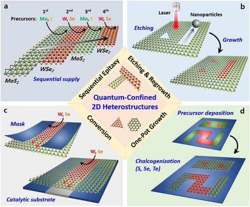
Table 1. Summary of the spatially controlled growth of 2D lateral and vertical heterostructures. Lateral and vertical heterostructures are denoted by A-B and A/B, respectively.
2. Spatially controlled growth of 2D quantum heterostructures
2.1. Sequential epitaxial growth
The growth of 2D heterostructures has been successfully reported in numerous reports, using various chemical vapor deposition (CVD)-based methods . The gas-phase CVD with solid-powder precursors or the metal–organic CVD (MOCVD) with all vapor phase precursors allows a large degree of freedom to control the growth of various 2D materials, further offering a scalable growth scheme. In particular, the selective and sequential supply of precursors is critical to achieving spatially controlled heterostructures via ‘sequential growth’. In addition to precursor control, for controlled spatial dimensions of crystal regions in the growth, it is also critical to regulate the nucleation (both density and location) to further select between lateral vs vertical growth processes. In this regard, a recent report has explained the preferred nucleation sites and kinetics of the vertical and lateral growth during the two-step CVD of 2D heterostructure based on MoS2 and WSe2 (Figure a) [Citation26]. The most critical factor determining the growth aspect is the diffusion barrier of gas-phase W1Sex clusters, enabling the growth of WSe2 either on the basal plane or edge of the prepared MoS2 (Figure b). Depending on the ratio between the transition metal and chalcogen flux (i.e. W/Se ratio), two types of W1Se1 and W1Se3 clusters can co-exist on the MoS2 surface in the vapor precursors. As shown in Figure a, W1Se1 active clusters with a high diffusion barrier (1.2 eV) are dominantly formed for a high W/Se ratio, which can induce the nucleation on top of the MoS2 basal plane to obtain vertical WSe2/MoS2 heterostructure. On the other hand, for the low W ratio, W1Se3 clusters are formed which have a relatively lower diffusion barrier (0.4 eV) and tend to diffuse towards the edge of MoS2, forming a lateral WSe2-MoS2 heterostructure. Similarly, the ratio between transition metal and chalcogen flux dictates lateral or vertical growth mode for various 2D heterostructures such as WS2/WSe2 [Citation26,Citation27], GaSe/MoS2 [Citation28], and MoSe2/WSe2 [Citation29]. In addition, the growth temperature affects the lateral vs vertical growth of 2D heterostructures [Citation36,Citation48,Citation58]. High-temperature (> 850 °C, roughly) growth promotes the extensive nucleation and growth of 2D crystals, resulting in a thermodynamic preference for vertical heterostructures. On the contrary, lower growth temperature favours a kinetic mechanism over a thermodynamic mechanism that stimulates lateral growth. Moreover, the defectiveness of the pre-formed crystal also determines the growth direction of the subsequent 2D structure [Citation36,Citation45]. If defects such as chalcogen vacancies exist in the 2D basal plane, the adsorption probability of precursors on the surface increases while promoting vertical growth rather than edge-mediated lateral growth [Citation36,Citation45].
Figure 3. Sequential epitaxial growth of vertical/lateral 2D heterostructures. (a, b) Determination of lateral/vertical growth aspects by the W/Se ratio during the two-step CVD [Citation26]. (a) Schematic of controllable lateral edge-mediated growth and vertical vdW epitaxy of heterostructures composed of MoS2 and WSe2 depending on the adsorption of various active clusters of W1Sex. (b) The diffusion barriers of W1Se3 and W1Se1 clusters on the edge/basal surface of the MoS2 layer. (c-e) Edge-mediated epitaxy of lateral WS2-WSe2-WS2 heterostructure [Citation31]. (c) Schematic of the edge-mediated epitaxy of lateral heterostructures. (d) High-resolution scanning transmission electron microscopy (STEM) image of the WS2-WSe2 lateral heterostructure (left). Magnified STEM image of the dashed red rectangle region (top right) and the corresponding atomic model (bottom right). (e) Scanning electron microscopy (SEM) images of the lateral WS2-WSe2-WS2 multi-heterojunction with ultra-narrow WSe2 width (∼35 and 13 nm) with different growth times (10 and 5 s). (f) vdW epitaxy of vertical MoS2/WS2 heterostructures [Citation37]. Flow-rate modulations of the metal-organicprecursors for the growth of (top) and a series of cross-sectional high-angle annular dark field (HAADF)-STEM images of the heterostructures depending on the flow rate (bottom) are shown. (g-i) Capillary force-driven rolling-up strategy for the fabrication of vdW superlattice [Citation39]. (g) Schematic illustration of the fabrication process of roll-up vdW superlattices. (h) STEM image of a rolled-up SnS2/WSe2 heterostructure. (i) STEM image (left) and corresponding energy-dispersive spectroscopy (EDS) mapping images (center: W, right: Sn) of the SnS2/WSe2 vdW superlattice.
![Figure 3. Sequential epitaxial growth of vertical/lateral 2D heterostructures. (a, b) Determination of lateral/vertical growth aspects by the W/Se ratio during the two-step CVD [Citation26]. (a) Schematic of controllable lateral edge-mediated growth and vertical vdW epitaxy of heterostructures composed of MoS2 and WSe2 depending on the adsorption of various active clusters of W1Sex. (b) The diffusion barriers of W1Se3 and W1Se1 clusters on the edge/basal surface of the MoS2 layer. (c-e) Edge-mediated epitaxy of lateral WS2-WSe2-WS2 heterostructure [Citation31]. (c) Schematic of the edge-mediated epitaxy of lateral heterostructures. (d) High-resolution scanning transmission electron microscopy (STEM) image of the WS2-WSe2 lateral heterostructure (left). Magnified STEM image of the dashed red rectangle region (top right) and the corresponding atomic model (bottom right). (e) Scanning electron microscopy (SEM) images of the lateral WS2-WSe2-WS2 multi-heterojunction with ultra-narrow WSe2 width (∼35 and 13 nm) with different growth times (10 and 5 s). (f) vdW epitaxy of vertical MoS2/WS2 heterostructures [Citation37]. Flow-rate modulations of the metal-organicprecursors for the growth of (top) and a series of cross-sectional high-angle annular dark field (HAADF)-STEM images of the heterostructures depending on the flow rate (bottom) are shown. (g-i) Capillary force-driven rolling-up strategy for the fabrication of vdW superlattice [Citation39]. (g) Schematic illustration of the fabrication process of roll-up vdW superlattices. (h) STEM image of a rolled-up SnS2/WSe2 heterostructure. (i) STEM image (left) and corresponding energy-dispersive spectroscopy (EDS) mapping images (center: W, right: Sn) of the SnS2/WSe2 vdW superlattice.](/cms/asset/ee564ece-0f4a-4e6b-a870-9a3d93789039/tmrl_a_2151852_f0003_oc.jpg)
Based on the aforementioned growth mechanisms, spatial-controllable lateral vs vertical 2D heterostructures can be obtained utilizing consecutively supplied gas-phase precursors during CVD. In this regard, this section handles two sequential epitaxial growth approaches for multi-heterojunction structures and superlattices: (i) the edge-mediated epitaxy process forming laterally covalent bonds between two different 2D materials and (ii) the vdW epitaxy process for vertical stacking of 2D materials by vdW interactions.
2.1.1. Lateral edge-mediated epitaxy
The selective evaporation of different precursors during powder-based CVD successfully induces sequential growth mode for lateral 2D heterostructures [Citation26–29,Citation33–35]. However, vacancy or alloy formation may occur along the pre-formed 2D crystal because of thermal decomposition and undesired chemical reactions at high temperatures during a thermal CVD process for heterostructures [Citation31,Citation36]. Furthermore, the nucleation of new crystals can be initiated from the growth template (sapphire, SiO2, or even on pre-grown crystals) rather than the edge of the existing 2D crystal. These issues, i.e. the thermal stability of the growth template and nucleation control at the desired position, represent a major obstacle in the delicate fabrication of single-layer-lateral hwteroatructures and superlattices. To address these issues, a novel method has been reported for achieving diverse lateral superlattices (Figure c) by using a modified thermal CVD process with a reverse flow of additional Ar gas from the substrate to the sources [Citation31]. By continuously flowing reverse Ar gas during the temperature change process, the high-temperature exposure of the existing monolayer grown on the substrate and the unintentional supply of chemical vapor precursors was minimized. Therefore, this approach allows the realization of lateral heterostructures with spatially-controlled interfaces without interfacial ternary or quaternary alloy regions (Figure d). In addition, supplying the source for a few seconds allows the width of the epitaxially grown 2D structure to be controlled on the nanometer scale (Figure e), showing the potential to fabricate laterally confined quantum wells or wires (QWs). In addition to the reverse flow scheme, thermally stable growth templates (e.g. multilayer PtTe2 up to 750 °C) can be employed to avoid both thermal decomposition and alloying of preformed 2D crystals, resulting in the growth of high-quality lateral 2D heterostructures [Citation36].
However, modulating the width in the nanoscale range is still challenging because the growth rate is generally fast and cannot be tuned delicately in the CVD process using powder-precursor vaporization [Citation31]. Therefore, a fine-tunable injection of vapor-phase precursors has been recommended. This has been recently demonstrated for lateral 2D WS2-WSe2 superlattices with coherent hetero-interfaces by utilizing metal–organic (MO) sources [Citation32]. Quantum-confined WSe2 monolayers down to 15 nm width with a relatively slow growth rate (i.e. 20 nm/min) was achieved and attributed to the significantly reduced flow rate of MO precursors. These advances highlight progress toward applying exceptional control over crystal growth and present a path toward realizing more complex and functional 2D quantum heterostructures.
2.1.2. Vertical vdW epitaxy
As mentioned above, in 2D vertical heterostructures, different atomic layers can be reassembled by vdW interactions with a minimized interfacial chemical bond between neighboring layers. Therefore, these are often called vdW heterostructures. vdW epitaxial growth mode allows obtaining not only the simple vdW heterostructure with two different 2D materials [Citation26–29,Citation38] but also the multi-heterojunctions by periodic repetition of source supplying during the CVD [Citation37]. Recently, an MOCVD-based growth method using MO precursors (Mo(CO)6, W(CO)6, and (C2H5)2S) as precursors has been reported to fabricate vdW MoS2/WS2 heterostructures (Figure f) [Citation37]. They epitaxially grew alternating MoS2 and WS2 monolayers on their respective surfaces by individually supplying the MO sources (Mo(CO)6, W(CO)6) with (C2H5)2S background flow after reaching the growth temperature. The growth order and the number of atomic layers were determined by the corresponding transition metal or chalcogen supply and the growth time. In addition, the vdW epitaxial growth was possible at a relatively low growth temperature (550 °C) due to the high vapor pressure of MO precursors. Other than MoS2/WS2 combination, this scheme can be expanded to TMD heterostructures with a graphene layer (WSe2/Graphene/WS2) as well as WS2/WSe2 and WSe2/MoS2/WS2 superlattices by selectively injecting other vapor sources [Citation37].
However, the MO precursor for MOCVD typically contains carbon atoms as part of precursor molecules that can cause carbon contamination, resulting in low quality and small domain size of the resulting crystal [Citation60]. Moreover, although the slow growth rate of the MOCVD method is effectively applied to the previously introduced lateral edge-epitaxy growth, the vdW epitaxy growth requires a long time to fill the surface with a large-area monolayer [Citation61]. Alternatively, a capillary force-driven rolling-up strategy has been proposed for producing vdW superlattices using pre-formed vertical vdW heterostructures with two different atomic layers (Figure g) [Citation39]. With this approach, two atomic layers can be stacked vertically at once into vdW superlattices with a more significant number of alternating layers (Figure h, i), extending into heterogeneous structures composed of different types of 2D atomic layers [Citation39]. In addition, 1D vdW heterostructures (or hybrid nanotubes) have recently been realized by the CVD method using single-walled carbon nanotubes (CNT) as a template [Citation62]. This resulted in the epitaxial growth of boron nitride or MoS2 shells around the CNT core, thus allowing the formation of single-crystalline boron nitride nanotubes and MoS2 nanotubes. This CVD-based epitaxy can expand the vast experimental space by combining other TMDs, nitrides, and oxides with CNTs [Citation63].
2.2. Etching and regrowth
As the previous section introduced, lateral or vertical heterostructures have been well established with sequential epitaxy growth. However, the production of high-density arrays of the 2D heterostructures with desired positions and dimensions is more practical and desirable for the design of quantum heterostructures. For example, to realize and control the quantum confinement effect within lateral heterostructures, we need to modulate the dimensions of the 2D semiconductors and the spacing between them as desired. Furthermore, the channel and contact dimensions should be scalable for 2D metal–semiconductor heterojunctions for realizing scaled atomically-thin circuits. Therefore, controlling the nucleation site for the second material growth in a two-step CVD technique is critical for the scalable production of quantum-confined heterostructures.
The partial etching of pre-deposited 2D materials followed by the growth of another 2D material (namely, the ‘Etching and Regrowth’ process) is the most widely used technique for the position-selective growth of 2D heterostructures (Figure ) [Citation64,Citation65]. The key to this method is to etch desirable spots on a prefabricated 2D thin film and then regrowth of different 2D materials from the treated local regions. The nucleation location (i.e. either on the basal or edge surface) can be controlled depending on the growth conditions, such as source concentration and growth temperature. Moreover, the adsorption energy of the precursors on the specific point can be engineered by the etching and surface treatment process on the pre-deposited 2D materials, resulting in lateral [Citation41,Citation44,Citation66] or vertical heterostructures [Citation45,Citation46]. For example, the standard lithography process [Citation64,Citation65] can unintentionally leave significant resist residue on the 2D substrates, becoming random nucleation centers leading to vertical growth. Therefore, residue-free treatments using laser [Citation41,Citation45], focused ion beam (FIB) [Citation46,Citation66], and metal particles [Citation44] have been suggested. In this section, we introduce the approaches for desired growth of heterostructures with an ultraclean interface.
Figure 4. Etching and regrowth process for the production of vertical/lateral 2D heterostructures. (a, b) Synthesis of periodic monolayer 2D heterostructures by laser-pattering and thermal etching process [Citation41]. (a) Schematic illustration of the growth process consists of laser patterning and thermal etching of the pre-deposited WS2 matrix followed by the growth of WSe2. (b) Optical microscopy (OM) image of a lateral heterostructure with WSe2 crystals embedded in a monolayer WS2 matrix. (c, d) Synthesis of chirality-controlled graphene nanoribbons (GNR) embedded in hBN [Citation44]. (c) Schematic showing the strategy to prepare GNRs with crystallographic edge orientations. Different particles of Ni or Pt etch nano-trenches with different edge topologies (Ni: zigzag, Pt: armchair) in an hBN layer. (d) AFM image of 1D GNR with zigzag terminations embedded in 2D hBN. (e, f) Vertical growth of VSe2 on WSe2 by incomplete etching of the WSe2 [Citation45]. (e) Schematic of the vertical growth process by laser irradiation. (f) OM image of periodic arrangements of VSe2/WSe2 heterostructure arrays.
![Figure 4. Etching and regrowth process for the production of vertical/lateral 2D heterostructures. (a, b) Synthesis of periodic monolayer 2D heterostructures by laser-pattering and thermal etching process [Citation41]. (a) Schematic illustration of the growth process consists of laser patterning and thermal etching of the pre-deposited WS2 matrix followed by the growth of WSe2. (b) Optical microscopy (OM) image of a lateral heterostructure with WSe2 crystals embedded in a monolayer WS2 matrix. (c, d) Synthesis of chirality-controlled graphene nanoribbons (GNR) embedded in hBN [Citation44]. (c) Schematic showing the strategy to prepare GNRs with crystallographic edge orientations. Different particles of Ni or Pt etch nano-trenches with different edge topologies (Ni: zigzag, Pt: armchair) in an hBN layer. (d) AFM image of 1D GNR with zigzag terminations embedded in 2D hBN. (e, f) Vertical growth of VSe2 on WSe2 by incomplete etching of the WSe2 [Citation45]. (e) Schematic of the vertical growth process by laser irradiation. (f) OM image of periodic arrangements of VSe2/WSe2 heterostructure arrays.](/cms/asset/7f8ca24b-ce71-4634-9686-f8678f1496fa/tmrl_a_2151852_f0004_oc.jpg)
A laser-pattering and an anisotropic thermal etching process have been effectively demonstrated to create periodic monolayer lateral heterostructures [Citation41]. The CVD-grown WS2 single crystal was first obtained, and then laser irradiations were used to make periodic arrays of point defects. Thermal annealing of the laser-patterned WS2 produced anisotropic thermal etching, resulting in WS2 with triangular hole arrays. After that, the holey WS2 template was employed as an epitaxial template to construct WS2-WSe2 mosaic heterostructures (Figure a). The preparation of atomically clean edges without residue to decrease random defects for unintentional nucleation is crucial to establishing a clean hetero-interface, which was made feasible by the laser treatment and thermal annealing procedure by preventing random etching. As a result, the monolayer WS2-WSe2 mosaic heterostructure array had a uniform, darker contrast in the optical image (Figure b), implying that the whole opening region of the triangular holes was filled. This strategy can be expanded to the growth of different heterostructures consisting of WS2-WSe2, WS2-MoS2, and WSe2-MoS2. Although this approach could produce triangular TMD islands at the desired position by laser patterning, the island dimensions were only on a micron scale rather than a nanometer scale, which is not small enough to exhibit quantum confinement of excitons or electrons.
In lateral 2D heterostructures, quantum-confined structures with nanoscale lateral dimensions have been realized for the first time by a metal nanoparticle (NP)-catalyzed cutting process [Citation44]. With this approach, chirality-controlled graphene nanoribbons (GNR) embedded in h-BN have been grown successfully using CVD within predefined zigzag or armchair trenches from metal NP etching in various reports [Citation42,Citation43,Citation44]. For instance, the Ni and Pt particles produced zigzag- and armchair-oriented nano-trenches in the hBN film (Figure c) [Citation44]. A subsequent CVD process creates in-plane heterostructures with lattice coherence, that is, the zigzag- and armchair-edge GNRs embedded in a continuous hBN sheet (Figure d). Together with the reduced dimensionality of GNR, its edges are passivated by hBN providing a robust platform to investigate their electrical transport [Citation44]. For example, depending on the zigzag and the armchair edge of GNRs, one can modulate the bandgap opening behaviors as well as their magnetic conductance. Hence, this integration scheme can provide the possibility to design heterostructures consisting of semiconducting GNRs passivated by high-quality insulating substrates for 2D circuits.
In addition to lateral 2D heterostructures, vertical heterostructures can also be formed using the etching and regrowth approach. The incomplete etching of the pre-formed 2D surface to produce defect sites like vacancy clusters, rather than the complete etching of the layers, is the critical factor in inducing vertical layer-by-layer synthesis of 2D materials at the partially etched positions on the 2D substrate. The use of focused ion beam (FIB) processing [Citation46] and laser irradiation [Citation45] have been suggested to control the preferential nucleation sites of 2D domains that are vertically grown, as shown in Figure e. In particular, the position-selective nucleation and growth of VSe2 crystals on large area WSe2 was successful at the periodically patterned defects array introduced by laser irradiation [Citation45]. The crystal size of VSe2 can be controlled by adjusting the reaction time, suggesting the controllability of the dimensions of the resultant heterostructure. Furthermore, this method is a universal strategy with the feasibility of fabricating other large-area TMDs heterostructure arrays, such as NiTe2, CoTe2, NbTe2, and VS2 on WSe2 as well as VSe2 on MoS2 [Citation45].
However, many of the heterostructures formed by ‘etching and regrowth’ have spatially confined features with at least a few micrometers rather than a few nanometers in dimensions [Citation21,Citation25–28]. Therefore, more precise patterning work is still required to reduce the size of heterostructures to realize a quantum-confinement effect. Furthermore, during the ‘etching and regrowth’ process, the large lattice mismatch or unintended polymer-based impurities on the 2D crystal can additionally trigger the vertical growth of the heterostructure [Citation40,Citation47,Citation48]. The graphene and MoS2 have a large lattice mismatch (> 28%) [Citation40], and the wet transfer process of graphene produces polymer impurities [Citation47,Citation48], which results in the nucleation of MoS2 on the graphene basal plane. Therefore, the resulting heterostructure possesses vertically overlapped junctions (∼2-200 nm in width) instead of a pure edge-to-edge connected structure. Recently, the direct preparation of a growth template (e.g. PtTe2) with a small lattice mismatch with MoS2 (< 3%) on an arbitrary substrate and without a transfer process [Citation36] has been suggested for the production of an edge-contact lateral heterostructure of 2D MoS2-PtTe2 with one-monolayer-thick lateral junction interface.
2.3. Post-synthetic conversion
The etching and regrowth approach described above has the benefit of enabling growth of desired 2D heterostructures at a chosen site. However, a delicate treatment for defect formation on the surface of the prepared 2D template is required to regulate the vertical or lateral growth direction. The ‘post-synthetic conversion process’ is a straightforward approach that induces atomic substitution based on the difference in thermal and chemical instability of 2D materials at high temperatures (> 700 °C). Several factors can modulate the relative thermodynamic instability, i.e. oxide masking layer [Citation49–51], catalytic substrates [Citation52,Citation53], the thickness of 2D homojunction [Citation67], and the existence of atomic dislocations [Citation55].
Patterning using a mask laser is a facile process to prepare heterostructures with desired patterns and is almost similar to the lithography process for conventional semiconductor production. After depositing an oxide (e.g. SiO2, Al2O3) mask layer over the 2D films, the supply of gaseous precursors at elevated temperatures can generate lateral 2D heterostructures in a scalable and controllable way (Figure a,b). [Citation49–51]. The exposed regions in the gas precursors are selectively converted to different 2D materials at high temperatures, and in this way, 2D lateral heterostructures such as MoS2-MoSe2 [Citation49], MoS2-Mo2C [Citation50], and graphene-hBN [Citation51] have been fabricated. However, several points must be considered from the thermodynamic perspective in this process. First, since sulfurization occurs at a lower temperature than the selenization, MoSe2 can be easily converted to MoS2, but the reverse reaction is not energetically favorable. In addition, the chemical reaction for the replacement of transition metal is not straightforward because of the high activation energy for the conversion.
Figure 5. Post-synthetic conversion process to achieve lateral 2D heterostructures. (a, b) Position-controlled conversion of 2D materials for the growth of lateral MoS2-MoS2 heterostructures [Citation49]. (a) Patterning and selective conversion of 2D materials using SiO2 masking layers for MoSe2-MoS2 heterostructures. (b) Raman mappings of MoS2-MoSe2 lateral heterojunction arrays formed within monolayer crystals by patterning and selective conversion processes. (c-e) Spatially controlled conversion process from hBN to graphene [Citation52, Citation53]. (c) Schematic illustrations for the conversion process of hBN on Pt substrate to produce 2D lateral heterostructure of graphene-hBN [Citation52]. (d, e) Schematic (d) and SEM image (e) of graphene quantum dots embedded in the hBN matrix, grown by the selective conversion on an array of the Pt nanoparticles. [Citation53]. (f) Schematic of the patterning process guided by misfit dislocations (marked as ‘T’) at the MoS2-WSe2 lateral heterojunction. (g) STEM images of MoS2 1D channels embedded within WSe2. (h) STEM image (left) and strain map (right) of a MoS2 1D channel formed from an intrinsic 5|7 dislocation in WSe2 [Citation55].
![Figure 5. Post-synthetic conversion process to achieve lateral 2D heterostructures. (a, b) Position-controlled conversion of 2D materials for the growth of lateral MoS2-MoS2 heterostructures [Citation49]. (a) Patterning and selective conversion of 2D materials using SiO2 masking layers for MoSe2-MoS2 heterostructures. (b) Raman mappings of MoS2-MoSe2 lateral heterojunction arrays formed within monolayer crystals by patterning and selective conversion processes. (c-e) Spatially controlled conversion process from hBN to graphene [Citation52, Citation53]. (c) Schematic illustrations for the conversion process of hBN on Pt substrate to produce 2D lateral heterostructure of graphene-hBN [Citation52]. (d, e) Schematic (d) and SEM image (e) of graphene quantum dots embedded in the hBN matrix, grown by the selective conversion on an array of the Pt nanoparticles. [Citation53]. (f) Schematic of the patterning process guided by misfit dislocations (marked as ‘T’) at the MoS2-WSe2 lateral heterojunction. (g) STEM images of MoS2 1D channels embedded within WSe2. (h) STEM image (left) and strain map (right) of a MoS2 1D channel formed from an intrinsic 5|7 dislocation in WSe2 [Citation55].](/cms/asset/91566b71-8b74-41f0-8711-9b8ef4a1d7e0/tmrl_a_2151852_f0005_oc.jpg)
In the case of the graphene-hBN heterostructures, the spatially controlled conversion process can be achieved not only on samples with a patterned SiO2 masking layer [Citation51] but also via a catalytic Pt substrate (Figure c) [Citation52,Citation53]. The Pt metal substrate allows the catalytic conversion of hBN to graphene under the CH4 atmosphere at 1000 °C. The high-temperature process triggers the decomposition of CH4 into carbon and hydrogen, followed by the simultaneous etching of hBN and the growth of graphene. This mask-free approach is beneficial to controlling the heterojunction more strictly because using the SiO2 mask layer cannot prevent the unintended atomic diffusion underneath the masking layer during the high-temperature process [Citation52]. Taking advantage of the spatially controllable technique using a catalytic substrate pattern, the same research group recently realized a lateral heterostructure composed of 0D graphene quantum dots embedded in a 2D hBN monolayer utilizing an array of Pt nanoparticles (Figure d) [Citation53,Citation54]. The spatial locations and dimensions of graphene quantum dots arrays are determined by the size (7-13 nm) and position of Pt nanoparticles (Figure e). Further, the hBN matrix passivates graphene edges to minimize unintentionally formed localized states, permitting preservation of pristine quantum confinement effects. Further, blue PL emission was also reported in their GQDs/hBN heterostructures, which was observed in samples fabricated under different conditions [Citation54].
Another interesting example of a self-driven conversion reaction is a dislocation-catalyzed approach has been introduced to epitaxially grow 1D nanoribbons of MoS2 embedded in a 2D WSe2 matrix [Citation55]. In this process, their lattice mismatch at lateral interfaces introduces misfit dislocations (marked as ‘T’ in Figure f), where the dislocation core exhibits high reactivity to growth precursors. This enables narrow nanoribbons to form behind an advancing dislocation core in the presence of a growth precursor. Although it requires the presence of a significant lattice mismatch at the interface to catalyze the formation of 1D nanoribbons, this method can produce very narrow nanoribbons with a width of a few nanometers or less. Controlling the dislocation spacing allows periodically spaced quantum-confined nanoribbons to be formed as 2D analogs to multilayer superlattices.
2.4. One-pot synthesis approach
This section introduces the one-pot synthesis approach for synthesis of vertical or lateral 2D heterostructures through precursor controls. The simultaneous growth process has the advantage of preventing unintended impurities or poisoning by exposure to the ambient atmosphere that may occur in the two-step CVD methods introduced in the previous sections. The different precursors for two different 2D materials in heterostructures are used for the delicate design of the target crystals. For example, simultaneous integration of metallic 1T’-MoTe2 and semiconducting 2H-MoTe2 has been reported by the conversion of two different precursors to MoTe2 with 2H or 1T’ phases during the tellurization process (Figure a) [Citation56]. This one-pot synthesis of two different polymorphs allowed the simultaneous construction and the distinctive hexagonal and monoclinic structures of the 2H and 1T′ phases at the atomic scale (Figure b). The lateral growth of 2D heterostructure is also possible by typical horizontal powder-based CVD, where two different transition-metal-based precursors are used under an S atmosphere for in-plane MoS2-WS2 p-n junction [Citation57,Citation58]. Probably due to the high vapor pressure of the Mo-based precursor [Citation68], MoS2 is preferentially formed, followed by the growth of WS2 [Citation57,Citation58]. In addition, the vertical heterostructures of Mo2C/graphene can be simultaneously prepared in the molten copper-catalyzed CVD process (Figure c) [Citation59]. Using a Mo-Cu alloy catalyst in a CH4 atmosphere allows the creation of high-quality Mo2C layers on a graphene monolayer (Figure d). Graphene functions as a diffusion barrier to the phase-segregated Mo within the vertical heterostructure, allowing the growth of ultrathin Mo2C on graphene. This approach is a promising strategy for obtaining superior transport characteristics through the ultraclean heterojunction of 2D vertical or lateral heterostructures. In comparison to the two-step growth procedure, this process requires more effort to be improved, especially concerning the scalability of the process. However, the delicate control of solid/vapor-phase precursors, growth template, and temperature may facilitate the production of novel 2D quantum heterostructures via this approach.
Figure 6. Simultaneous, one-pot synthesis of vertical or lateral 2D heterostructures. (a, b) Simultaneous integration of metallic 1T’-MoTe2 and semiconducting 2H-MoTe2 by tellurization of patterned precursors of MoO3 and MoO3-x [Citation56]. (a) Schematic for the growth of lateral heterostructure of 1T’−2H MoTe2 heterojunction. (b) STEM image of the heterojunction (inset: SEM image). (c, d) Direct synthesis of vertical 2D Mo2C/graphene heterostructure using molten Mo-Cu alloy catalyst and high CH4 concentration during the CVD [Citation59]. (c) Schematic of the growth process, and (d) OM image of Mo2C crystals on a graphene monolayer.
![Figure 6. Simultaneous, one-pot synthesis of vertical or lateral 2D heterostructures. (a, b) Simultaneous integration of metallic 1T’-MoTe2 and semiconducting 2H-MoTe2 by tellurization of patterned precursors of MoO3 and MoO3-x [Citation56]. (a) Schematic for the growth of lateral heterostructure of 1T’−2H MoTe2 heterojunction. (b) STEM image of the heterojunction (inset: SEM image). (c, d) Direct synthesis of vertical 2D Mo2C/graphene heterostructure using molten Mo-Cu alloy catalyst and high CH4 concentration during the CVD [Citation59]. (c) Schematic of the growth process, and (d) OM image of Mo2C crystals on a graphene monolayer.](/cms/asset/0dbe6dbe-40bf-4716-9d2e-66a1ce8a0afc/tmrl_a_2151852_f0006_oc.jpg)
3. Potential optoelectronic applications
3.1. Light-emitting diodes (LEDs)
The realization of lateral and vertical 2D heterostructures can provide versatile optoelectronic device applications that traditional heterostructures based on bulk materials may not allow with similar functionality. One such application is the LED, which can provide an effective way to probe excitonic optical responses by controlling carrier recombination [Citation69]. Similar to the conventional LED using III-V compound semiconductors of InxGayN, the QW structure fabricated by employing various 2D materials in the vertical heterostructure can perform as LED (Figure a) [Citation70]. Multiple 2D materials, e.g. metallic graphene, insulating hBN, and semiconducting monolayer MoS2, are stacked together for the superlattice of the QW. Due to the strong Coulomb interaction in monolayer MoS2, the recombination of excitons leads to light emission efficiently at a wavelength from 600 to 700 nm. The hBN inserted between the luminescent MoS2 and graphene electrodes minimizes the light emission quenching, suggesting that the delicate design of 2D vertical heterostructures will further enhance quantum emission efficiency. Also, appropriate selection of 2D semiconductors in the QW can allow control in the emission wavelength and enhance the emission intensity of the fabricated devices. For further improvement, multiple QW structure can be introduced by vertical vdW epitaxy growth.
Figure 7. Promising applications of vertical or lateral 2D heterostructures. (a, b) Light-emitting diode (LED) based on vertical heterostructures composed of hBN, graphene, and TMD layers [Citation70]. (a) Schematic of band alignments, and (b) OM image showing the red-light emission from the LED of vdW heterostructure. (c, d) Self-powered photodetector fabricated using p-n Bi2Te3-WSe2 heterostructure [Citation38]. (c) OM image of the photodetector, and (d) photoresponse of the corresponding junction device with different light wavelengths (375, 520, 980, and 1550 nm). (e, f) Tunneling transistor application realized by using graphene quantum dots (GQD) embedded in hBN layers [Citation53]. (e) Modeling of the single-electron charging effect. (f) Conductance (G) as a function of Vg and Vb for a device with 10 nm-sized graphene quantum dots (QDs) measured at T = 0.25 K. (g, h) Quantum-confined electronic states in MoS2/WSe2 heterobilayers [Citation82]. (g) STM image and (h) conductance map taken along the yellow line in (g) for voltages in the valence band-edge region. (i, j) Lateral metal-semiconductor junction (MSJ) comprised of MoS2 and PtTe2 synthesized by two-step growth [Citation36]. (i) Schematic (top) and OM image (bottom) of the heterostructure. (j) Output electrical characteristics of MSJ transistor where the carriers are injected from PtTe2 (red) and Ti (blue). (k) The proposed quantum-confined heterostructure based on 0D QDs and 2D matrix with type-I band alignment, (left) the atomic schematic, and (right) the band structure.
![Figure 7. Promising applications of vertical or lateral 2D heterostructures. (a, b) Light-emitting diode (LED) based on vertical heterostructures composed of hBN, graphene, and TMD layers [Citation70]. (a) Schematic of band alignments, and (b) OM image showing the red-light emission from the LED of vdW heterostructure. (c, d) Self-powered photodetector fabricated using p-n Bi2Te3-WSe2 heterostructure [Citation38]. (c) OM image of the photodetector, and (d) photoresponse of the corresponding junction device with different light wavelengths (375, 520, 980, and 1550 nm). (e, f) Tunneling transistor application realized by using graphene quantum dots (GQD) embedded in hBN layers [Citation53]. (e) Modeling of the single-electron charging effect. (f) Conductance (G) as a function of Vg and Vb for a device with 10 nm-sized graphene quantum dots (QDs) measured at T = 0.25 K. (g, h) Quantum-confined electronic states in MoS2/WSe2 heterobilayers [Citation82]. (g) STM image and (h) conductance map taken along the yellow line in (g) for voltages in the valence band-edge region. (i, j) Lateral metal-semiconductor junction (MSJ) comprised of MoS2 and PtTe2 synthesized by two-step growth [Citation36]. (i) Schematic (top) and OM image (bottom) of the heterostructure. (j) Output electrical characteristics of MSJ transistor where the carriers are injected from PtTe2 (red) and Ti (blue). (k) The proposed quantum-confined heterostructure based on 0D QDs and 2D matrix with type-I band alignment, (left) the atomic schematic, and (right) the band structure.](/cms/asset/598ff10d-9f52-4e23-a088-489b916b42d2/tmrl_a_2151852_f0007_oc.jpg)
Regarding lateral heterostructures, the in-plane p-n diode using WSe2-MoS2 heterojunction [Citation34,Citation35] with type-I band alignment can also be applied to function as an LED. The strain induced by lattice mismatch causes changes in the band structures of both WSe2 and MoS2. Under the misfit strain, the conduction band minimum (CBM) of WSe2 exhibits downward band bending, whereas that of MoS2 undergoes upward band bending, while also upshifting the valence band maximum (VBM) of MoS2 at the heterointerface [Citation15]. Hence, the misfit strain at the heterointerface leads to the conversion of type II to type I band alignment for the light emission, indicating that synthetically obtained heterostructure can modulate the band distributions/alignments [Citation35,Citation69]. Comparably, the localized disorder states can exhibit peculiar electroluminescence in an LED operation, which has been reported at in-plane hBN-graphene heterointerface [Citation54]. Although the practical use of 2D quantum heterostructures in LEDs is still limited for the time being due to their low emission efficiency, the use of various heterostructures and materials will allow the fabrication of devices with desired properties in the future.
3.2. Photodetectors
Photodetection over a wide range of the electromagnetic spectrum, from UV to IR, has also been achieved in 2D materials based photodetectors with various active layers with different band gaps [Citation38,Citation71]. Specifically, the 2D material-based heterostructures, e.g. 2D p-n diodes, can act as a self-powered broadband photodetector because of the effective and fast separation of photo-excited carriers owing to the built-in potential [Citation38]. The CVD-grown 2D vertical heterostructure further allows the enhanced performance of photodetectors because of intense coupling between the two 2D layers and the prevention of contaminants at the heterointerface as compared to their counterparts fabricated by mechanical exfoliation [Citation71]. For example, self-powered broadband photodetectors have been demonstrated based on epitaxially grown vertical WSe2/Bi2Te3 p-n heterojunction (Figure c) [Citation38]. The synthetic heterojunction-based photodetector also has a low dark current with broadband responsivity, which is promising for highly sensitive photodetection (Figure d). Similarly, lateral heterostructures of WS2-MoS2 [Citation57] and WSe2-MoSe2 [Citation29,Citation33] also offer novel potential for p-n junction-based photodetectors.
3.3. Single electron tunneling transistors
Because graphene is a zero-bandgap material, its band gap opening must be performed to fabricate a graphene transistor with a high on-to-off current ratio. Many attempts have been conducted to introduce the bandgap into graphene by tailoring it into quantum structures with lower dimensions (e.g. nanoribbon, constriction, and quantum dots) [Citation16–20]. In addition, based on the low dimensional structures and vdW integration of graphene, the single electron tunneling (SET) transistor can also be realized [Citation72,Citation73].
These SET transistors have also been expanded in TMD materials. Unlike graphene, the inversion symmetry is broken in the semiconducting TMD monolayers. The monolayers with individual valleys in momentum space at points K and K’ in the Brillouin region, together with the presence of time-reversal symmetry, facilitates the momentum state of electrons to be used for novel qubit architectures [Citation74–76]. Some theoretical studies have suggested that the spin and valley states of gate-defined quantum dots can be used as quantum bits in 2D TMDs [Citation77,Citation78]. More recently, several groups have experimentally shown the possibilities of realizing SET transistors by stacking exfoliated flakes [Citation23–25]. However, studies using 2D monolayers and heterostructures grown over large areas have remained to be conducted, and the large-scale integration is obviously challenging compared with conventional 3D semiconductors.
Recently, research on the SET transistors has been reported, where the device was fabricated using the layer of graphene quantum dots (GQDs) arrays incorporated into a CVD-grown hBN monolayer matrix. The quantum dot array grown by conversion of hBN (discussed in section 2.3) was used as a channel, combined with hBN tunneling barriers and graphene electrodes. In this tunneling transistor, at a small bias voltage between the source and drain was applied, electrons can tunnel through quantum-confined states to create the current flow where the charge can be detected, as shown in Figure e. Interestingly, the fabricated GQDs have chemical bonds with insulating hBN, allowing the reduction of the number of localized states along the quantum dot edge. Such edge-passivated GQDs/hBN heterostructures may open further opportunities for designing lateral QW structures.
The utilization of the quantum-confined states in vdW heterostructures is particularly interesting. The vertical combination of two 2D monolayers can generate new electronic states due to the hybridization of electronic states between the layers. Rotational misalignment between lattices of the same monolayers or lattice mismatch between different monolayers leads to moiré patterns when forming bilayers. Starting with twist graphene bilayers, these patterns have been studied not only in homogeneous hBN and TMD bilayers but also in heterobilayers made with other monolayer combinations, such as graphene/hBN and various TMD/TMD combinations. Quantum-confined electronic states have also been reported in the moiré patterns of MoS2/WSe2 heterobilayers on graphene synthesized by CVD. The potential variation in the moiré structures arising from lattice mismatch (3.7%) gives rise to confined states with discrete energy levels that could be studied by scanning tunneling spectroscopy at liquid helium (5 K) temperature. Figure h shows a conductance map along the yellow line (A-B-C-A) across such a moiré unit cell (as indicated in Figure g). Discrete confined states are observed at the AB stacking location (B: ABW, C: ABSe labeled in Figure g). The significant modulation of band edge positions observed in these 2D heterogeneous bilayers can be utilized as a platform for quantum simulation or forming qubits. However, observing confined states at room temperature is very challenging. More sophisticated work is needed to determine the effects of band-edge shifts and concomitant band-edge states in device applications.
3.4. 2d semimetal-based source/drain in transistors
The conventional preparation of 2D metal–semiconductor junction (MSJ) by deposition of 3D metals (e.g. Ti/Au) on 2D semiconductors typically results in a defect-rich interface because 2D TMDs are vulnerable to the high-energy process that may form glassy layers, vacancies, and voids [Citation45,Citation79]. The defect-induced gap states also pin the Fermi level of MSJ at the shifted charge neutrality; hence, the Schottky barrier height at the MSJ interface cannot be effectively modulated by the selection of 3D metals with different work functions [Citation79]. In contrast, the 2D heterostructures based on 2D (semi-)metal and 2D semiconductors can provide an ultraclean, sharp 2D MSJ interface compared to the conventional 3D/2D MSJ [Citation36,Citation45,Citation47,Citation48,Citation50,Citation56].
In particular, vertically produced 2D/2D heterostructures with metallic VSe2 and semiconducting WSe2 allow WSe2 transistors to have a high current density (Figure e, f) [Citation45]. In addition, the lateral MSJ heterostructure consisting of metallic PtTe2 and semiconducting MoS2 monolayer can have a sub-1 nm transfer length (LT) due to its edge-to-edge connected atomically thin interface (Figure i) [Citation36]. The reduced dimensionality with fewer interfacial defects can weaken the Fermi-level pinning effect, enabling the reduced Schottky barrier dimensions for high-performance 2D transistors, as indicated by the higher current density of 2D-2D PtTe2-MoS2 MSJ higher than that using Ti contact electrodes (Figure j) [Citation36]. The synthesized edge-contact MSJ of 1T’−2H MoTe2 also offers a novel strategy for constructing high-performance transistors. The reported field-effect transistor with edge contact showed higher mobility than that of the MSJ with 3D metal contacts [Citation56].
Furthermore, the use of Dirac material, i.e. graphene, as a source in the 2D transistor has also enabled realization of subthreshold swing values smaller than the thermionic limit (< 60 mV/dec at room temperature), which is known as Dirac-source field-effect transistor [Citation80,Citation81]. The Fermi level of Dirac material can be changed depending on the gate voltages while shifting the contact barrier height between 2D semiconductor (e.g. MoS2) and Dirac-source (i.e. graphene). Since the transport is still relies on the thermionic emission process, a high on-state current density is possible in the transistor, which promises an innovative approach for low-power and high-performance vdW electronics.
4. Challenges and future outlooks
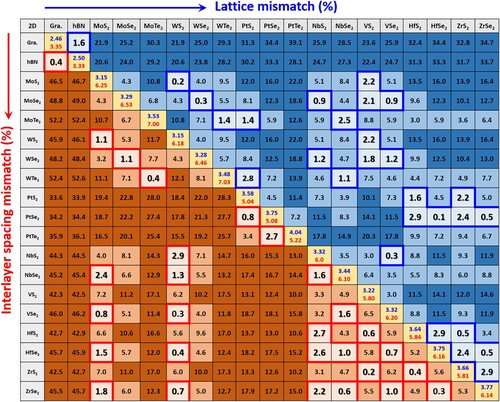
Spatially controlled 2D heterostructures with new and unique physical properties have been synthesized through various developments in materials engineering, as we presented in the previous sections. The lattice and interlayer spacing mismatch between 2D materials shown in Figure is one of the obstacles in the epitaxial growth of monolithic 2D vertical and lateral heterostructures. Despite different lattice constants and spacings, a strong chemical bond can form a heterojunction between the two materials. However, the large lattice or spacing mismatch leads to numerous mismatch-related defects, such as mismatch dislocations, strain, and interfacial disturbances at the heterointerface. Therefore, one should consider the unit cell sizes of 2D materials for designing defect-free 2D heterostructures.
Figure 8. Lattice and interlayer spacing mismatch between TMDs. The values in yellow boxes on the central diagonal represent the lattice constant (top, blue) and interlayer spacing (bottom, red) of the TMDs, respectively. The values in the lower right (blue) and upper left boxes (red) are the lattice and spacing mismatch between each TMD, of which values less than 3% are highlighted. The lattice mismatch was calculated by simply considering the in-plane lattice distances of each unit cell of two materials.
For more novel fabrication of 2D heterostructures, we also suggest introducing the following strategies or structures. First, for a universal and reproducible production of laterally stitched TMD heterostructures, finding a reliable and compatible processing option is recommended for uniform nucleation. The random nucleation of TMD flakes, typically by a horizontal powder-based CVD approach[Citation83], results in relatively small grain growth of semiconducting layers. The limited nucleation at the edge of TMDs followed by lateral growth may lead to forming of a full-grown coplanar heterostructure with larger grains. In this respect, MOCVD with a minimal growth rate in a vertical reactor [Citation84,Citation85] can be a favorable choice to promote uniform nucleation and layer-by-layer growth for the 2D heterostructures.
Second, finding a way to minimize thermal damage is important during the production of heterostructures in the case of sequential epitaxial growth. During synthesizing the second material by two-step CVD, the pre-deposited 2D material could be degraded thermally, especially under the reducing atmosphere containing H2, producing a large density of vacancies along the growth template. Furthermore, this may also lead to the creation of atomically mixed alloys by introducing different atomic species in the second growth step instead of compositionally distinct heterostructures [Citation86]. Considering that thermal degradation typically produces chalcogen vacancies rather than transition-metal vacancies in 2D TMDs [Citation87,Citation88], the growth of TMDs with the same chalcogen atom is better for reducing any chances of forming chalcogen alloys during the two-step CVD (e.g. MoS2-WS2 instead of MoS2-MoSe2 heterostructures). In addition, single-crystalline 2D materials rather than polycrystalline are more beneficial as a growth template, given their higher thermal stability [Citation87,Citation89].
Third, the minimization of device variability and realization of high-yield processes are much desired to afford a practical technological option. Owing to the ultrathin body of vdW TMDs, even minor mechanical stress during the transfer process can induce various defects, such as cracks, wrinkles, and ripples at the layer [Citation90,Citation91]. The handling by the polymeric support layer also degrades the TMD layer by leaving behind polymer residues [Citation92]. Additionally, numerous TMDs [Citation93,Citation94] show structural vulnerability against air exposure because humidity and oxygen can readily oxidize their surface. Hence, optimizing the fully automated transfer and device fabrication process under air-free conditions should be adapted for the devices using the quantum heterostructures.
Finally, we would like to note that the type-I lateral heterostructures with quantum-confined superlattice or QW structure have not yet been achieved by CVD methods. Recently, quantum confinement in 2D TMD materials has been investigated for single photon emission based on naturally or artificially occurring defects [Citation95–98]. However, it is necessary to realize deterministic nanoscale exciton confinement in planar structures for better compatibility with microdevices. We propose that 0D TMD quantum confined structures distributed in a distinct 2D TMD layer can be a viable solution for achieving quantum confinement of excitons in lateral heterostructures, as shown in Figure k. To realize quantum confinement of 2D excitons at the nanoscale, the following requirements should be satisfied; (i) precise and deterministic control of quantum dot position and bandgap, (ii) proper band alignment (type-I) between matrixes and quantum dots (Figure k, right), and (iii) seamless and defect-free interfaces between quantum dots and matrix material. This heterostructure will provide opportunities for integrating quantum-confined TMDs with conventional optical and optoelectronic devices, such as LEDs, micro-resonators, and high Q cavities. We believe these new approaches will significantly contribute to a breakthrough in quantum photonic technologies for quantum cryptography and communications.
5. Conclusions
This paper reviews the recent advances in spatially-controlled growth of 2D vertical/lateral heterostructures for quantum optoelectronic applications. We first cover the ‘sequential epitaxial growth’ of 2D heterostructures, where the vertical and lateral growth direction of subsequently grown 2D materials may be dominantly determined by the chalcogen-to-metal ratio, growth temperature and defect densities at the preformed 2D crystal. The ‘etching and regrowth’ and ‘post-synthetic conversion’ processes are established for selective control of the nucleation sites for the pattered heterostructures arrays or 1D-like confined heterostructures. The ‘one-pot synthesis’ of 2D heterostructures is possible by using different precursors during the growth at the same time. The spatially controlled 2D lateral/vertical heterostructures can be used in different optical and electrical applications by using their novel physical phenomena or band alignments. In particular, the strain induced by the lattice mismatch could result in the band edge shift, enabling its type-I band alignments of p-n diodes for LED. The increased coupling between 2D materials and the ultraclean interface allows the fabrication of highly efficient photodetectors and low-series resistances at 2D MSJ in transistors. In addition, the confined nanostructures of QW or QDs across the 2D matrix and the lateral heterointerfaces result in new electronic states in these synthetic heterostructures, which may be useful for potential tunneling transistors or quantum photonic applications.
Acknowledgments
D.J. and G.K. acknowledge primary support for this work by the Asian Office of Aerospace Research and Development (AOARD) of the Air Force Office of Scientific Research (AFOSR) FA2386-20-1-4074 and FA2386-21-1-4063. S.S acknowledges support for this work by Basic Science Research Program through the National Research Foundation of Korea (NRF) funded by the Ministry of Education (grant number 2021R1A6A3A14038492).
Disclosure statement
No potential conflict of interest was reported by the author(s).
Additional information
Funding
References
- Stanford MG, Rack PD, Jariwala D. Emerging nanofabrication and quantum confinement techniques for 2D materials beyond graphene. npj 2D Mat Appl. 2018;2(1):20. doi:10.1038/s41699-018-0065-3.
- Chowdhury T, Sadler EC, Kempa TJ. Progress and prospects in transition-metal dichalcogenide research beyond 2D. Chem Rev. 2020;120(22):12563–12591. doi:10.1021/acs.chemrev.0c00505.
- Chen P, Zhang Z, Duan X, et al. Chemical synthesis of two-dimensional atomic crystals, heterostructures and superlattices. Chem Soc Rev. 2018;47(9):3129–3151. doi:10.1039/C7CS00887B.
- Li J, Liang J, Yang X, et al. Controllable preparation of 2D vertical van der waals heterostructures and superlattices for functional applications. Small. 2022;18(22):2107059. doi:10.1002/smll.202107059.
- Lim H, Yoon SI, Kim G, et al. Stacking of two-dimensional materials in lateral and vertical directions. Chem Mater. 2014;26(17):4891–4903. doi:10.1021/cm502170q.
- Kim G, Shin HS. Spatially controlled lateral heterostructures of graphene and transition metal dichalcogenides toward atomically thin and multi-functional electronics. Nanoscale. 2020;12(9):5286–5292. doi:10.1039/C9NR10859A.
- Li J, Zhong YL, Zhang D. Excitons in monolayer transition metal dichalcogenides. J Phys: Condens Matter. 2015;27(31):315301. doi:10.1088/0953-8984/27/31/315301.
- Gan ZX, Liu LZ, Wu HY, et al. Quantum confinement effects across two-dimensional planes in MoS2 quantum dots. Appl Phys Lett. 2015;106(23):233113. doi:10.1063/1.4922551.
- Mukherjee S, Maiti R, Katiyar AK, et al. Novel colloidal MoS2 quantum dot heterojunctions on silicon platforms for multifunctional optoelectronic devices. Sci Rep. 2016;6(1):29016. doi:10.1038/srep29016.
- Wei G, Czaplewski DA, Lenferink EJ, et al. Size-tunable lateral confinement in monolayer semiconductors. Sci Rep. 2017;7(1):3324. doi:10.1038/s41598-017-03594-z.
- Golovynskyi S, Bosi M, Seravalli L, et al. Mos2 two-dimensional quantum dots with weak lateral quantum confinement: intense exciton and trion photoluminescence. Surfaces Inter. 2021;23:100909. doi:10.1016/j.surfin.2020.100909.
- Cadiz F, Robert C, Courtade E, et al. Exciton diffusion in WSe2 monolayers embedded in a van der waals heterostructure. Appl Phys Lett. 2018;112(15):152106. doi:10.1063/1.5026478.
- Pan S, Kong W, Liu J, et al. Understanding spatiotemporal photocarrier dynamics in monolayer and bulk MoTe2 for optimized optoelectronic devices. ACS Appl Nano Mat. 2019;2(1):459–464. doi:10.1021/acsanm.8b02008.
- Goodman AJ, Lien DH, Ahn GH, et al. Substrate-dependent exciton diffusion and annihilation in chemically treated MoS2 and WS2. J Phys Chem C. 2020;124(22):12175–12184. doi:10.1021/acs.jpcc.0c04000.
- Giannazzo F, Sonde S, Nigro RL, et al. Mapping the density of scattering centers limiting the electron mean free path in graphene. Nano Lett. 2011;11(11):4612–4618. doi:10.1021/nl2020922.
- Danneau R, Wu F, Craciun MF, et al. Shot noise in ballistic graphene. Phys Rev Lett. 2008;100(19):196802. doi:10.1103/PhysRevLett.100.196802.
- Sarma S D, Adam S, Hwang EH, et al. Electronic transport in two-dimensional graphene. Rev Mod Phys. 2011;83(2):407–470. doi:10.1103/RevModPhys.83.407.
- Terrés B, Dauber J, Volk C, et al. Disorder induced Coulomb gaps in graphene constrictions with different aspect ratios. Appl Phys Lett. 2011;98(3):032109. doi:10.1063/1.3544580.
- Borunda MF, Hennig H, Heller EJ. Ballistic versus diffusive transport in graphene. Phys Rev B. 2013;88(12):125415. doi:10.1103/PhysRevB.88.125415.
- Terrés B, Chizhova LA, Libisch F, et al. Size quantization of Dirac fermions in graphene constrictions. Nat Commun. 2016;7(1):11528. doi:10.1038/ncomms11528.
- Smithe KKH, English CD, Suryavanshi SV, et al. Intrinsic electrical transport and performance projections of synthetic monolayer MoS 2 devices. 2D Mater. 2016;4(1):011009. doi:10.1088/2053-1583/4/1/011009.
- Pisoni R, Lee Y, Overweg H, et al. Gate-defined one-dimensional channel and broken symmetry states in MoS2 van der Waals heterostructures. Nano Lett. 2017;17(8):5008–5011. doi:10.1021/acs.nanolett.7b02186.
- Pisoni R, Lei Z, Back P, et al. Gate-tunable quantum dot in a high quality single layer MoS2 van der Waals heterostructure. Appl Phys Lett. 2018;112(12):123101. doi:10.1063/1.5021113.
- Boddison-Chouinard J, Bogan A, Fong N, et al. Gate-controlled quantum dots in monolayer WSe2. Appl Phys Lett. 2021;119(13):133104. doi:10.1063/5.0062838.
- Jing F-M, Zhang Z-Z, Qin G-Q, et al. Gate-controlled quantum dots based on 2D materials. Adv Quant Technol. 2022;5(6):2100162. doi:10.1002/qute.202100162.
- Li F, Feng Y, Li Z, et al. Rational kinetics control toward universal growth of 2D vertically stacked heterostructures. Adv Mater. 2019;31(27):1901351. doi:10.1002/adma.201901351.
- Wang D, Zhang Z, Huang B, et al. Few-Layer WS2–WSe2 lateral heterostructures: influence of the Gas precursor selenium/tungsten ratio on the number of layers. ACS Nano. 2022;16(1):1198–1207. doi:10.1021/acsnano.1c08979.
- Zou Z, Liang J, Zhang X, et al. Liquid-Metal-Assisted growth of vertical GaSe/MoS2 p–n heterojunctions for sensitive self-driven photodetectors. ACS Nano. 2021;15(6):10039–10047. doi:10.1021/acsnano.1c01643.
- Gong Y, Lei S, Ye G, et al. Two-step growth of two-dimensional WSe2/MoSe2 heterostructures. Nano Lett. 2015;15(9):6135–6141. doi:10.1021/acs.nanolett.5b02423.
- Sutter P, Huang Y, Sutter E. Nanoscale integration of two-dimensional materials by lateral heteroepitaxy. Nano Lett. 2014;14(8):4846–4851. doi:10.1021/nl502110q.
- Zhang Z, Chen P, Duan X, et al. Robust epitaxial growth of two-dimensional heterostructures, multiheterostructures, and superlattices. Science. 2017;357(6353):788–792. doi:10.1126/science.aan6814.
- Xie S, Tu L, Han Y, et al. Coherent, atomically thin transition-metal dichalcogenide superlattices with engineered strain. Science. 2018;359(6380):1131–1136. doi:10.1126/science.aao5360.
- Najafidehaghani E, Gan Z, George A, et al. 1D p–n junction electronic and optoelectronic devices from transition metal dichalcogenide lateral heterostructures grown by one-pot chemical vapor deposition synthesis. Adv Funct Mater. 2021;31(27):2101086. doi:10.1002/adfm.202101086.
- Li M-Y, Pu J, Huang J-K, et al. Self-aligned and scalable growth of monolayer WSe2–MoS2 lateral heterojunctions. Adv Funct Mater. 2018;28(17):1706860. doi:10.1002/adfm.201706860.
- Zhang C, Li M-Y, Tersoff J, et al. Strain distributions and their influence on electronic structures of WSe2–MoS2 laterally strained heterojunctions. Nat Nanotechnol. 2018;13(2):152–158. doi:10.1038/s41565-017-0022-x.
- Song S, Yoon A, Ha J-K, et al. Atomic transistors based on seamless lateral metal-semiconductor junctions with a sub-1-nm transfer length. Nat Commun. 2022;13(1):4916. doi:10.1038/s41467-022-32582-9.
- Jin G, Lee C-S, Okello OFN, et al. Heteroepitaxial van der Waals semiconductor superlattices. Nat Nanotechnol. 2021;16(10):1092–1098. doi:10.1038/s41565-021-00942-z.
- Liu H, Zhu X, Sun X, et al. Self-Powered broad-band photodetectors based on vertically stacked WSe2/Bi2Te3 p–n heterojunctions. ACS Nano. 2019;13(11):13573–13580. doi:10.1021/acsnano.9b07563.
- Zhao B, Wan Z, Liu Y, et al. High-order superlattices by rolling up van der Waals heterostructures. Nature. 2021;591(7850):385–390. doi:10.1038/s41586-021-03338-0.
- Liu X, Balla I, Bergeron H, et al. Rotationally commensurate growth of MoS2 on epitaxial graphene. ACS Nano. 2016;10(1):1067–1075. doi:10.1021/acsnano.5b06398.
- Zhang Z, Huang Z, Li J, et al. Endoepitaxial growth of monolayer mosaic heterostructures. Nat Nanotechnol. 2022;17(5):493–499. doi:10.1038/s41565-022-01106-3.
- Lu X, Yang W, Wang S, et al. Graphene nanoribbons epitaxy on boron nitride. Appl Phys Lett. 2016;108(11):113103. doi:10.1063/1.4943940.
- Chen L, He L, Wang HS, et al. Oriented graphene nanoribbons embedded in hexagonal boron nitride trenches. Nat Commun. 2017;8(1):14703. doi:10.1038/ncomms14703.
- Wang HS, Chen L, Elibol K, et al. Towards chirality control of graphene nanoribbons embedded in hexagonal boron nitride. Nat Mater. 2021;20(2):202–207. doi:10.1038/s41563-020-00806-2.
- Li J, Yang X, Liu Y, et al. General synthesis of two-dimensional van der Waals heterostructure arrays. Nature. 2020;579(7799):368–374. doi:10.1038/s41586-020-2098-y.
- Heilmann M, Deinhart V, Tahraoui A, et al. Spatially controlled epitaxial growth of 2D heterostructures via defect engineering using a focused He ion beam. npj 2D Materials and Applications. 2021;5(1):70. doi:10.1038/s41699-021-00250-z.
- Zhao M, Ye Y, Han Y, et al. Large-scale chemical assembly of atomically thin transistors and circuits. Nat Nanotechnol. 2016;11(11):954–959. doi:10.1038/nnano.2016.115.
- Hong W, Shim GW, Yang SY, et al. Improved electrical contact properties of MoS2-graphene lateral heterostructure. Adv Funct Mater. 2019;29(6):1807550. doi:10.1002/adfm.201807550.
- Mahjouri-Samani M, Lin M-W, Wang K, et al. Patterned arrays of lateral heterojunctions within monolayer two-dimensional semiconductors. Nat Commun. 2015;6(1):7749. doi:10.1038/ncomms8749.
- Choi S, Kim YJ, Jeon J, et al. Scalable Two-dimensional lateral metal/semiconductor junction fabricated with selective synthetic integration of transition-metal-carbide (Mo2C)/-dichalcogenide (MoS2). ACS Appl Mater Interfaces. 2019;11(50):47190–47196. doi:10.1021/acsami.9b13660.
- Gong Y, Shi G, Zhang Z, et al. Direct chemical conversion of graphene to boron- and nitrogen- and carbon-containing atomic layers. Nat Commun. 2014;5(1):3193. doi:10.1038/ncomms4193.
- Kim G, Lim H, Ma KY, et al. Catalytic conversion of hexagonal boron nitride to graphene for in-plane heterostructures. Nano Lett. 2015;15(7):4769–4775. doi:10.1021/acs.nanolett.5b01704.
- Kim G, Kim S-S, Jeon J, et al. Planar and van der Waals heterostructures for vertical tunnelling single electron transistors. Nat Commun. 2019;10(1):230. doi:10.1038/s41467-018-08227-1.
- Kim G, Ma KY, Park M, et al. Blue emission at atomically sharp 1D heterojunctions between graphene and h-BN. Nat Commun. 2020;11(1):5359. doi:10.1038/s41467-020-19181-2.
- Han Y, Li M-Y, Jung G-S, et al. Sub-nanometre channels embedded in two-dimensional materials. Nat Mater. 2018;17(2):129–133. doi:10.1038/nmat5038.
- Zhang Q, Wang X-F, Shen S-H, et al. Simultaneous synthesis and integration of two-dimensional electronic components. Nature Electronics. 2019;2(4):164–170. doi:10.1038/s41928-019-0233-2.
- Wu W, Zhang Q, Zhou X, et al. Self-powered photovoltaic photodetector established on lateral monolayer MoS2-WS2 heterostructures. Nano Energy. 2018;51:45–53. doi:10.1016/j.nanoen.2018.06.049.
- Gong Y, Lin J, Wang X, et al. Vertical and in-plane heterostructures from WS2/MoS2 monolayers. Nat Mater. 2014;13(12):1135–1142. doi:10.1038/nmat4091.
- Geng D, Zhao X, Chen Z, et al. Direct synthesis of large-area 2D Mo2C on in situ grown graphene. Adv Mater. 2017;29(35):1700072. doi:10.1002/adma.201700072.
- Schaefer CM, Caicedo Roque JM, Sauthier G, et al. Carbon incorporation in MOCVD of MoS2 thin films grown from an organosulfide precursor. Chem Mater. 2021;33(12):4474–4487. doi:10.1021/acs.chemmater.1c00646.
- Kang K, Xie S, Huang L, et al. High-mobility three-atom-thick semiconducting films with wafer-scale homogeneity. Nature. 2015;520(7549):656–660. doi:10.1038/nature14417.
- Xiang R, Inoue T, Zheng Y, et al. One-dimensional van der Waals heterostructures. 2020;367(6477):537–542. doi:10.1126/science.aaz2570.
- Gogotsi Y, Yakobson BI. Nested hybrid nanotubes. 2020;367(6477):506–507. doi:doi:10.1126/science.aba6133.
- Levendorf MP, Kim C-J, Brown L, et al. Graphene and boron nitride lateral heterostructures for atomically thin circuitry. Nature. 2012;488(7413):627–632. doi:10.1038/nature11408.
- Liu Z, Ma L, Shi G, et al. In-plane heterostructures of graphene and hexagonal boron nitride with controlled domain sizes. Nat Nanotechnol. 2013;8(2):119–124. doi:10.1038/nnano.2012.256.
- Li H, Li P, Huang J-K, et al. Laterally stitched heterostructures of transition metal dichalcogenide: chemical vapor deposition growth on lithographically patterned area. ACS Nano. 2016;10(11):10516–10523. doi:10.1021/acsnano.6b06496.
- Li H, Wu X, Liu H, et al. Composition-modulated Two-dimensional semiconductor lateral heterostructures via layer-selected atomic substitution. ACS Nano. 2017;11(1):961–967. doi:10.1021/acsnano.6b07580.
- Zhou J, Lin J, Huang X, et al. A library of atomically thin metal chalcogenides. Nature. 2018;556(7701):355–359. doi:10.1038/s41586-018-0008-3.
- Wada N, Pu J, Takaguchi Y, et al. Efficient and chiral electroluminescence from in-plane heterostructure of transition metal dichalcogenide monolayers. Adv Funct Mater. 2022;32(40):2203602. doi:10.1002/adfm.202203602.
- Withers F, Del Pozo-Zamudio O, Mishchenko A, et al. Light-emitting diodes by band-structure engineering in van der waals heterostructures. Nat Mater. 2015;14(3):301–306. doi:10.1038/nmat4205.
- Qiu Q, Huang Z. Photodetectors of 2D materials from ultraviolet to terahertz waves. Adv Mater. 2021;33(15):2008126. doi:10.1002/adma.202008126.
- Ihn T, Güttinger J, Molitor F, et al. Graphene single-electron transistors. Mater Today. 2010;13(3):44–50. doi:10.1016/S1369-7021(10)70033-X.
- Liu X, Hersam MC. 2D materials for quantum information science. Nat Rev Mat. 2019;4(10):669–684. doi:10.1038/s41578-019-0136-x.
- Xiao D, Liu G-B, Feng W, et al. Coupled spin and valley physics in monolayers of ${{MoS}}_{2}$ and other group-VI dichalcogenides. Phys Rev Lett. 2012;108(19):196802. doi:10.1103/PhysRevLett.108.196802.
- Xu X, Yao W, Xiao D, et al. Spin and pseudospins in layered transition metal dichalcogenides. Nat Phys. 2014;10(5):343–350. doi:10.1038/nphys2942.
- Kormányos A, Zólyomi V, Drummond ND, et al. Monolayer MoS${}_{2}$: trigonal warping, the {Γ}$ valley, and spin-orbit coupling effects. Phy Rev B. 2013;88(4):045416. doi:10.1103/PhysRevB.88.045416.
- Novoselov KS, Mishchenko A, Carvalho A, et al. 2D materials and van der Waals heterostructures. Science. 2016;353(6298):aac9439. doi:10.1126/science.aac9439.
- Kormányos A, Zólyomi V, Drummond ND, et al. Spin-orbit coupling, quantum dots, and qubits in monolayer transition metal dichalcogenides. Phys Rev X. 2014;4(1):011034. doi:10.1103/PhysRevX.4.011034.
- Song S, Sim Y, Kim S-Y, et al. Wafer-scale production of patterned transition metal ditelluride layers for two-dimensional metal–semiconductor contacts at the Schottky–Mott limit. Nat Electron. 2020;3(4):207–215. doi:10.1038/s41928-020-0396-x.
- Qiu C, Liu F, Xu L, et al. Dirac-source field-effect transistors as energy-efficient, high-performance electronic switches. Science. 2018;361(6400):387–392. doi:10.1126/science.aap9195.
- Liu F, Qiu C, Zhang Z, et al. Dirac electrons at the source: breaking the 60-mV/decade switching limit. IEEE Trans Electron Devices. 2018;65(7):2736–2743. doi:10.1109/TED.2018.2836387.
- Pan Y, Fölsch S, Nie Y, et al. Quantum-confined electronic states arising from the moiré pattern of MoS2–WSe2 heterobilayers. Nano Lett. 2018;18(3):1849–1855. doi:10.1021/acs.nanolett.7b05125.
- Kim H, Ovchinnikov D, Deiana D, et al. Suppressing nucleation in metal–organic chemical vapor deposition of MoS2 monolayers by alkali metal halides. Nano Lett. 2017;17(8):5056–5063.
- Tang L, Li T, Luo Y, et al. Vertical chemical vapor deposition growth of highly uniform 2D transition metal dichalcogenides. Acs Nano. 2020;14(4):4646–4653.
- Lee DH, Sim Y, Wang J, et al. Metal–organic chemical vapor deposition of 2D van der Waals materials—The challenges and the extensive future opportunities. APL Mater. 2020;8(3):030901. doi:10.1063/1.5142601.
- Zhang Z, Gong Y, Zou X, et al. Epitaxial growth of two-dimensional metal–semiconductor transition-metal dichalcogenide vertical stacks (VSe2/MX2) and their band alignments. ACS Nano. 2019;13(1):885–893. doi:10.1021/acsnano.8b08677.
- Pitthan E, Gerling ERF, Feijó TO, et al. Annealing response of monolayer MoS2 grown by chemical vapor deposition. ECS J Solid State Sci Technol. 2019;8(4):P267–P270. doi:10.1149/2.0061904jss.
- Song S, Kim S-Y, Kwak J, et al. Electrically robust single-crystalline WTe2 nanobelts for nanoscale electrical interconnects. Adv Sci. 2019;6(3):1801370. doi:10.1002/advs.201801370.
- Cai S, Zhao W, Zafar A, et al. Photoluminescence characterization of the grain boundary thermal stability in chemical vapor deposition grown WS2. Mater Res Express. 2017;4(10):106202. doi:10.1088/2053-1591/aa8f82.
- Zhang T, Fujisawa K, Granzier-Nakajima T, et al. Clean transfer of 2D transition metal dichalcogenides using cellulose acetate for atomic resolution characterizations. ACS Appl Nano Mat. 2019;2(8):5320–5328. doi:10.1021/acsanm.9b01257.
- Kim C, Yoon M-A, Jang B, et al. Damage-free transfer mechanics of 2-dimensional materials: competition between adhesion instability and tensile strain. NPG Asia Mater. 2021;13(1):44. doi:10.1038/s41427-021-00311-1.
- Liang J, Xu K, Toncini B, et al. Impact of post-lithography polymer residue on the electrical characteristics of MoS2 and WSe2 field effect transistors. Adv Mater Interfaces. 2019;6(3):1801321.
- Naylor CH, Parkin WM, Gao Z, et al. Large-area synthesis of high-quality monolayer 1T’-WTe 2 flakes. 2D Mater. 2017;4(2):021008. doi:10.1088/2053-1583/aa5921.
- Yang L, Wu H, Zhang W, et al. Anomalous oxidation and its effect on electrical transport originating from surface chemical instability in large-area, few-layer 1T′-MoTe2 films. Nanoscale. 2018;10(42):19906–19915. doi:10.1039/C8NR05699D.
- Chakraborty C, Kinnischtzke L, Goodfellow KM, et al. Voltage-controlled quantum light from an atomically thin semiconductor. Nat Nanotechnol. 2015;10(6):507–511. doi:10.1038/nnano.2015.79.
- He Y-M, Clark G, Schaibley JR, et al. Single quantum emitters in monolayer semiconductors. Nat Nanotechnol. 2015;10(6):497–502. doi:10.1038/nnano.2015.75.
- Koperski M, Nogajewski K, Arora A, et al. Single photon emitters in exfoliated WSe2 structures. Nat Nanotechnol. 2015;10(6):503–506. doi:10.1038/nnano.2015.67.
- Srivastava A, Sidler M, Allain AV, et al. Optically active quantum dots in monolayer WSe2. Nat Nanotechnol. 2015;10(6):491–496. doi:10.1038/nnano.2015.60.