
 ?Mathematical formulae have been encoded as MathML and are displayed in this HTML version using MathJax in order to improve their display. Uncheck the box to turn MathJax off. This feature requires Javascript. Click on a formula to zoom.
ABSTRACT
The Kikuchi bands arise from Bragg diffraction of incoherent electrons scattered within a crystalline specimen and can be observed in both the transmission and reflection modes of scanning electron microscopy (SEM). Converging, rocking, or grazing incidence beams must be used to generate divergent electron sources to obtain the Kikuchi pattern. This paper report the observation of Kikuchi pattern from SEM images of an exceptional rotating crystal with continuous rotation in the local crystal direction and satisfying cylindrical symmetry, named a cylindrically symmetric rotating crystal. By retracing the Kikuchi line pattern, it is possible to obtain the lattice structure information of the presented sample from the conventional SEM images. SEM images of cylindrically symmetric rotating crystals reflect the interactions between electrons and the sample in both the real- and momentum-space. It is a very interesting and representative new case for the study of the contrast mechanism in SEM.
GRAPHICAL ABSTRACT
IMPACT STATEMENT
Unveiling a unique rotating crystal, the study expands the understanding of scanning electron microscopy (SEM) contrast mechanisms by simultaneously capturing real-space morphology and momentum-space lattice information in a single image.
1. Introduction
Scanning electron microscopy (SEM) is one of the most commonly used modern scientific instruments, producing images of a sample surface by scanning it with a focused electron beam [Citation1]. The complex interaction between electron beam and sample surface produces various signals at each image pixel detected and displayed on a display unit that scans over the sample in parallel with the beam scanning. When the focused beam hits a focal point on the specimen, the signal intensity is measured by a detector to integrate the dwell time and is expressed as the pixel’s brightness in a digital image. This gray-level image is related to particular characteristics of the specimen and can be interpreted as various image contrasts caused by different mechanisms [Citation2,Citation3]. Therefore, it is crucial to understand the mechanism of contrast and its numerical meaning in SEM. Any new contrast mechanism discovered in SEM has the potential to expand its range of applications and usefulness in research and industrial production.
The most common mode of SEM operation is the raster scan [Citation4] of a specimen’s surface, in which energetic electrons are focused into a beam with a small spread, and the beam is incident on the sample in the same direction and scanned point-by-point. With this parallel incident electron beam, the digital image obtained is a real space image, where each pixel in the image corresponds to a location in the real space of the sample.
Throughout the historical development of SEM and its applications, various contrast mechanisms in raster scanning mode have been understood. Electrons interact with the sample surface to produce electron signals containing various information about the sample surface, in which the sample’s surface morphology and composition are essential [Citation5,Citation6]. The most common types of contrast are topographic contrast [Citation7–10] and composition/elemental contrast [Citation11–14], which are applicable and available for almost all specimens and provide the basis for SEM image formation. In addition, some special contrast mechanisms, such as electric field [Citation15,Citation16], magnetic [Citation17,Citation18], electron charging [Citation19–21], and plasmon gain [Citation22–24] contrast exist in certain types of materials and are closely related to specific material properties. All these contrasts can be well-explained by the particle nature of electrons.
SEM also produces diffraction contrast [Citation25–31], which usually reflects the specimen’s structural information, such as grain orientation, local texture, phase identification and distribution. Only electrons’ wave nature can explain the diffraction contrast’s formation mechanism. To observe a relatively complete diffraction pattern of a crystalline or polycrystalline sample using an SEM, one needs to change the operating mode of the SEM.
Two modes of SEM operation are used to obtain relatively complete diffraction patterns. The first is to collect backscattered electrons from different directions exiting the sample surface when electrons are incident on the sample at a large angle. This mode is the electron backscattered diffraction (EBSD) mode [Citation32], in which the incident electron beam enters the sample at a glancing angle and is scattered by the atoms inside the sample. Many of these, called backscattered electrons, escape from the sample surface because of multiple large angle scattering [Citation33–35]. In the process of leaving the sample, the backscattered electrons that meet the Bragg diffraction condition [Citation36], 2dsinθ = λ, are diffracted from a particular family of crystal planes of the sample, forming two conical surfaces with the central axis perpendicular to the family of crystal planes. The two conical surfaces intersect with the receiving screen to form a bright band called the Kikuchi band. The centerline of each Kikuchi band corresponds to the intersection of the expanded crystal plane corresponding to this Bragg diffraction with the receiving screen [Citation37]. Because each Kikuchi band is associated with Bragg diffraction from one side of a set of lattice planes, it has been an effective method for studying a substance’s crystal structure [Citation38] since it was observed by Kikuchi in transmission electron microscopy (TEM) as early as 1928 [Citation39].
The second mode to observe a complete diffraction contrast is to scan the single crystal sample surface by changing the incidence direction of the electron beam so that it forms a continuously changing angle about the crystal direction of the sample [Citation40]. Vibrating the electron beam causes it to diffract with the lattice at a particular location on the sample surface in different directions to form a Kikuchi pattern. This is the electron channeling pattern (ECP) mode [Citation41]. The EBSD and ECP modes both form a Kikuchi pattern by continuously changing the angle between the emission or incident electrons and the sample’s crystal orientation and subsequently analyzing the Kikuchi patterns to obtain the crystal structure information [Citation42,Citation43]. Therefore, the pixel position change of the acquired Kikuchi patterns in both EBSD and ECP modes corresponds to the momentum change of the electrons in the plane normal to the sample surface.
It is evident that the SEM raster scan mode is used to acquire information in the real space of the sample, while the ECP and EBSD modes are used to acquire information about the sample in the momentum space. It is an intriguing prospect that a sample could be investigated in both the real- and momentum-space from a single SEM image, but we have achieved this using a so-called cylindrical symmetric rotating crystal. In this sample, the crystal direction at a local position continuously rotates and satisfies cylindrical symmetry with respect to the central position. With this sample, we have observed both the contrasts of the surface morphology and a complete Kikuchi pattern in one SEM image measured in the raster scan mode. The contrast produced by the overlap of the real- and the momentum-space in this unique SEM image combines the particle and wave nature of electrons interacting with the sample bulk and surface. Subsequently, the fundamental reason for observing the Kikuchi pattern in the SEM images is revealed by analyzing the cylindrical symmetric rotating crystal using the EBSD technique. Finally, we point out that one Kikuchi pattern in the EBSD Kikuchi pattern matrix map is unique, having the ‘same’ Kikuchi pattern as the SEM image observed using the cylindrical symmetric rotating crystal. In this case, the SEM image is a Banach fixed point of the EBSD Kikuchi map.
2. Material and methods
2.1. Rotating crystal film preparation
Amorphous films with a 30 nm thickness were prepared by DC magnetron sputtering (Shibaura Mechatronics, CFS-4EP-LL i-Miller, Japan) on a sapphire substrate at room temperature. Sputtering targets consisting of In2O3 and SiO2 were used. The ratio of Si/In in the sputtering target was 2.3 at. %, corresponding to 1 wt. % in terms of SiO2/(In2O3 + SiO2). The sputtering target and the substrate were separated by 160 mm in the sputtering system. InSiO films were generated by a plasma at 200 W under a mixed atmosphere of argon and oxygen at a 1:1 gas flow ratio and 0.25 Pa total pressure. This gas flow ratio was determined to produce electrically stable InSiO films resistant to thermal stress [Citation44–46]. In situ SEM observations were performed to obtain images of dynamic crystallization along a precisely fixed observation area. The InSiO films were heated in situ to 300 °C in the SEM environment. shows typical results of SEM and EBSD observations of InSiO films after crystallographic heating.
2.2. SEM measurements
In situ SEM observations were performed by combining the Gatan Murano heating sub-stage and Hitachi SU5000 Schottky SEM (Hitachi, Japan). This combined system allowed us to obtain images of crystallization dynamically along a precisely fixed observation area.
2.3. EBSD measurements
Diffraction patterns were collected using a JSM-IT800 SEM (JEOL, Japan) equipped with a CCD detector in high resolution (1244 × 1024) mode. The setup geometry was held constant with a 10.0 ± 0.1 mm working distance. The imaging parameters were a 15 kV accelerating voltage, ~20 nA beam current, and 0.1 ms dwell time. After collecting high-resolution EBSDs from each material, all patterns collected were exported as TIF images.
3. Results
3.1. Kikuchi pattern imaging mechanism in SEM
We now consider the case shown in , where the electron beam is scanned over a rotating crystal for which the local crystal orientation is rotated. As the electron beam is scanned over the sample, its angle with respect to the local crystal orientation changes, and therefore the backscattered electron signals collected by an SEM detector also change. Because θ = θB (where θB is the Bragg angle) at points A and B, the angle between the incident electron beam and the local crystal direction is θ < θB between these positions and collects enhanced backscattered electron signals. However, θ > θB before and after A and B, so the backscattered electron signals decrease relative to their values at A and B.
Figure 1. (a) Geometric variation of the angle between the incident electron beam and the local crystal orientation while scanning a rotating crystal sample. During any line scan through the center of a rotating crystal, the angle θ between the incident electron beam and the local crystal orientation varies from greater than θB to less than θB. The two symmetrical positions a and B are where θ = θB. This variation results in a change in the backscattered electron signal intensity during the line scan. (b) Schematic diagram of the crystal plane rotation of a rotating crystal and the corresponding Kikuchi pattern in the sample region.
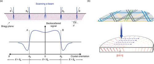
If a complete two-dimensional raster is scanned over the crystal, as typically done in SEM, then the other lattice planes also contribute to the contrast, and the resulting signal map, the ECP, shows contrast bands from all planes or normal to the surface. The width of each band is twice the appropriate Bragg angle of the set of lattice planes from which it comes, and the angle between the bands is the angle between the corresponding sets of lattice planes. Thus, this ECP has lattice symmetry in the region being examined, and if a rotating crystal with cylindrical symmetry is scanned, it is possible to observe a Kikuchi pattern.
shows a schematic of the cylindrically symmetric rotating crystal sample, in which the crystal’s local orientation at different positions changes slowly and continuously. The relative local crystal orientation refers to the center of the sample satisfying cylindrical symmetry. As seen in , the [001] crystal orientation deflection gradually increases from its normal position in the center of the crystal (perpendicular to the film plane) as the circular crystallographic front moves outward, as illustrated by the sketch of the [001] direction in the cross-section of the figure. In other words, during crystal growth, the unit cell rotates uniformly along the cross-section passing through the center point of the circular crystal film, and the unit cell (if traced along any radial outward direction of crystal growth) rotates permanently around an axis located in the plane of the film.
Therefore, the electron beam is scanned perpendicular to the sample’s surface in the conventional SEM mode. The incident electrons diffract with the atomic lattice having different orientations at different landing positions, making it possible to observe the Kikuchi pattern in the entire sample scan image when the sample satisfies the special rotational structure described above. Although the contrast has been described in terms of the backscattered electron signal, any of the electron signals from the specimen (i.e. secondary, specimen current, or, if the sample is thin enough, the transmitted beam) show equivalent contrast features, and whichever is most convenient can be used.
3.2. Observed SEM and EBSD images
In this work, the rotating crystal is prepared based on bixbyite type In2O3. shows the crystallization of InSiO during the annealing process. The films grown on these substrates are partially crystallized, with a significant volume of material remaining amorphous. When the films are annealed at 300 °C, the amorphous films gradually crystallize, grow into approximately 1–2 μm diameter round crystal islands, and form distinct Kikuchi patterns. These rotating crystal islands are circular structures that grow quasi-isotropically and radially from individual nucleation sites.
Figure 2. (a) The observed SEM images of InSiO film detected by backscattered electrons during the crystallization process of amorphous film at 300 °C. (b) The observed EBSD-normal direction (ND) images in the same region.
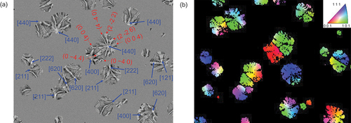
It is reasonable to assume that these rotating crystal islands begin growing from randomly distributed nucleation sites in the amorphous film, followed by two-dimensional growth from the center. In some cases, the nucleation site is isolated. In other cases, the growth stops because of a neighboring crystalline site. This is a typical island nucleation and growth process in a thin film, as reported in Refs. [Citation47–50]. These crystalline islands all exhibit distinct Kikuchi-like diffraction patterns in the SEM images. All the observed Kikuchi patterns belong to the cubic (bixbyite type) In2O3 structure. In addition, these crystalline islands exhibit different Kikuchi patterns in the SEM images, implying that each crystalline island’s crystallographic orientation is different. The observed Kikuchi pattern has several characteristic patterns, which suggest several preferred nucleation directions in the crystallization process, similar to those observed in previous studies [Citation51].
For example, crystallization usually starts with the formation of a crystalline nucleus with the In2O3 structure and with the [440] direction approximately normal to the film plane. The observed Kikuchi patterns easily reveal the preferred lattice orientation with the [440] orientation. This orientation is deduced from the In2O3 crystal Kikuchi pattern, which allows indices to be assigned to the Kikuchi band (using the Kikuchi pattern spherical projection of In2O3). The nuclei always show strong lattice curvature, as indicated by the small inter-contour distances between the (hkl) and (-h-k-l) Kikuchi bands, always appearing in pairs. Six major Kikuchi bands are visible in the SEM image shown in from the two sets of (2–26)-type planes: two sets of (2–22)-type planes, one (4–40)-type plane, and one (004)-type plane. Different sets of Kikuchi bands possess different bandwidths, intersecting in a ‘pole’ and forming a bright, complex hexagon. Similarly, the Kikuchi patterns for the [400], [222] zone axis with different characteristics are shown in the SEM image. The indexes for these bands are also labeled in the SEM image.
These Kikuchi patterns can be assigned to the rotating crystal with zone axes of [211], [222], [400], [440], and [622], where the crystal planes are marked in . We note that there is no Kikuchi pattern originating from the SiO2 structure, indicating that the Si atoms are soluble in the In2O3 matrix at the rotating crystal region. This result is consistent with InSiO film crystallization information acquired by X-ray diffraction (XRD) [Citation44], in which no XRD peak originated from crystalline SiO2.
We note that the predicted inelastic mean free paths (IMFPs) of bixbyite In2O3 at an incident electron energy of 15 keV using the TPP-2 M [Citation52] and TPP-LASSO-S [Citation53] empirical formulae are 16.1 and 16.5 nm, respectively. In addition, the Gaussian process regressor [Citation54,Citation55] machine learning model trained using well-established databases of solid material optical constants [Citation56–62] and IMFP databases [Citation63–71] resulted in a predicted bixbyite In2O3 IMFP of 15.9 nm at 15 keV incident electron energy. These predicted values are less than 1/2 of the InSiO film thickness, so it can be assumed that the contrast of the SEM images shown in originates from the InSiO film.
The different colors in the EBSD-normal direction (ND) maps in indicate the different orientations inside the rotating crystal islands. Orientation changes are visible within one island, and there is only one snowflake-like crystal ‘grain’ without any significant crystal misorientation boundary in each rotational crystal island. The image analysis shows that the central area of every rotational crystal island spherulite has a homogeneous orientation rotational velocity, branching into larger features with a slightly different orientation rotational velocity upon further growth. However, it should be noted that such a rotational crystal is still a whole grain, which is entirely different from the previously reported ones [Citation51,Citation72] with spherulites that are spherical (or circular) structures consisting of fibers growing radially and quasi-isotopically from a single nucleation point. The orientation of the different island centers varies within a limited number of orientations, including [211], [222], [440], [400], and [622] zone axes, consistent with the observation from our XRD experiment [Citation44].
3.3. TEM cross-sectional images
For further verification, the cross-sectional profile of the presented rotating crystal island for the [400] direction is provided in using the TEM technique. The lattice structure of the sapphire substrate, as well as the crystalline region, is clearly seen to belong to the lattice structure of cubic bixbyite In2O3.
Figure 3. (a) The cross-section of the rotating crystal island for the [111] direction, in which the central region is the rotating crystal island, and the neighbouring two sides are the amorphous region. (b) Enlarged cross-sections of the crystal region in the TEM image. The blue lines are for the (100) plane in the sapphire substrate, and the red lines are for the (400) plane in InSiO. (c) Fast Fourier transforms (FFTs) of the selected regions (marked by the dashed white rectangles in b in the cross-sectional images. The blue lines are for the (100) plane in the sapphire substrate, the red dashed lines are for the [400] direction in momentum-space after FFT in InSiO, and the dashed black lines are for horizontal reference. The angles between the [400] direction in InSiO and (100) plane in the sapphire substrate are labeled in these images.
![Figure 3. (a) The cross-section of the rotating crystal island for the [111] direction, in which the central region is the rotating crystal island, and the neighbouring two sides are the amorphous region. (b) Enlarged cross-sections of the crystal region in the TEM image. The blue lines are for the (100) plane in the sapphire substrate, and the red lines are for the (400) plane in InSiO. (c) Fast Fourier transforms (FFTs) of the selected regions (marked by the dashed white rectangles in b in the cross-sectional images. The blue lines are for the (100) plane in the sapphire substrate, the red dashed lines are for the [400] direction in momentum-space after FFT in InSiO, and the dashed black lines are for horizontal reference. The angles between the [400] direction in InSiO and (100) plane in the sapphire substrate are labeled in these images.](/cms/asset/1b391653-6cab-47f8-8a74-52bafbef9f10/tstm_a_2230870_f0003_oc.jpg)
In these cross-sectional TEM images, the angle between the (400) plane in the InSiO cross-section (marked by the red line), and the (100) plane in sapphire (marked by the blue line), varies with the TEM image observation location. Fast Fourier transforms (FFTs) of these cross-sectional images are performed to demonstrate the variation of the (400) plane in the InSiO cross-section, as shown in the bottom panel (). The red dashed lines are for the [400] direction in momentum-space after FFT, the blue lines are for the (100) plane in the sapphire substrate, and the black dashed lines are for horizontal reference.
The angles after FFT between the [400] direction of InSiO in momentum-space and the (100) plane in the sapphire substrate are measured and shown in . The angle is 97.0 degrees when the observation location of the TEM image is at the leftmost edge of the rotating crystal island. As the observation location gradually moves to the right, the corresponding angle gradually decreases at an approximately constant rate, reaching 83.1 degrees when the observation location has moved to the rotating crystal island’s rightmost edge (680 nm from the leftmost edge). The (400) crystal plane in the rotating crystal island clearly rotates continuously along the cross-sectional direction at a rotational speed of roughly 20.4 °/μm as the observation location changes in the rotating crystal island.
Additionally, the lattice constant of the rotating lattice island is determined by measuring the (400) lattice plane distance. The average lattice spacing of the (400) crystalline planes measured using these TEM cross-sectional images is 0.2513 nm. Thus, the lattice constant determined from this lattice spacing by the equation is 10.055 Å for rotating crystal islands. This value is almost identical to the value measured using the XRD technique (10.048 Å ± 0.018 Å).
However, the lattice constants of both measured rotating islands are slightly smaller than the original lattice constant of 10.094 Å ± 0.012 Å for polycrystalline In2O3 films prepared in the same way, indicating a 0.4% unit lattice shrinkage. Because tensile stresses usually expand the lattice parameters in the films, the shrinkage observed here is caused by Si dopants. Although a small amount of Si does not significantly change the crystal structure of cubic bixbyite, the lattice parameters of the rotating crystalline InSiO island differ significantly from those of pure In2O3.
The interface between the low-density amorphous InSiO and the high-density InSiO rotating crystal islands is observed in the TEM cross-sectional images of the two rotating island edge regions (). This sub-interface can also be seen as the crystallization front located at the film’s middle depth. It is ahead of the crystallization front near the surface and the front near the substrate.
A significant amount of densification by shrinking must occur along the glass/crystal interface during crystallization when this front propagates as a whole parallel to the interface between the film sample and substrate. For thin films, the increase in density occurs preferentially in the direction perpendicular to the free surface, which means there is a gradient in density when moving towards the surface. This directionality occurs because the change in film shape is unrestricted only in that direction [Citation73] once the shrinkage rate along the highly diffuse crystalline front is slower than the propagation rate at the crystallographic interface. From the analogy of heterogeneous epitaxial crystal growth, it is expected that a type of dislocation is formed on the crystalline side of this interface, with mismatches appearing periodically to compensate for the lattice parameter mismatch [Citation74]. An additional half-plane appears on the crystalline side because of the crystalline state’s small interatomic distance (higher density).
According to speculation in Ref. [Citation72], these unpaired dislocations initially appearing at the interface remain in the growing crystal volume. They may act as a built-in geometrically necessary dislocation (GND), which generates continuous lattice bending and is responsible for forming rotating crystal structures. A near-edge X-ray absorption fine structure (NEXAFS) measurement at the BL01B1 beamline of the SPring-8 synchrotron radiation facility was performed to verify this speculation [Citation44]. The resulting NEXAFS spectra of the completely annealed rotating crystal InSiO sample demonstrate that the octahedral structure of the InO6 units and tetrahedral SiO4 units are preserved. The small number of tetrahedral SiO4 units in the InO6 octahedral network presumably causes local distortion in the bixbyite In2O3 matrix. These local distortions, in turn, become the GNDs necessary to rotate the InSiO thin-film crystal, which makes the InSiO film internally bend the crystal lattice planes around an axis lying in the film plane.
A similar phenomenon was found earlier for crystal growth in amorphous films of different substances [Citation51,Citation72–76], in which the local crystal orientation rotates uniformly along the cross-section that passes through the center point of the circular crystal film. Therefore, they are referred to as transrotational crystals. However, for the InSiO thin-film crystal used here, the relative local crystal orientation refers to the center of this sample possessing cylindrical symmetry in addition to continuous rotation in the local crystal direction. The details are discussed in the following section.
It is also notable that the observed interface propagation boundary differs slightly from the assumptions made in previous reports [Citation72,Citation73]. These previous reports assumed that the crystallization front near the surface leads to the crystallization front near the substrate. Here, the observed crystallization front near the surface and the crystallization front near the substrate both lag behind the crystallization front in the medium depth region of the thin InSiO film. This difference could lead to crystals that rotate in two different ways, as depicted in the TEM cross-sectional images. First, the crystal surface rotates along the radial direction, that is, on the polar angle. At the same time, the crystal also rotates around its own center, that is, azimuthally. This results in a circular-symmetric pattern leading to the observed SEM Kikuchi pattern.
4. Discussion
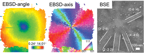
shows SEM and EBSD measurements of rotating crystal islands. The backscattered electron (BSE) images of the rotating crystal island show clear Kikuchi patterns, indicating that the central region of the rotating crystal island should be near the [440] zone axis. It is clear that six major visible Kikuchi bands arise from the two sets of (2–26)-type planes: two sets of (2–22)-type planes, one (4–40)-type plane, and one (00–4)-type plane. Different sets of Kikuchi bands possess different bandwidths, intersecting in a ‘pole’ that forms a complex polygon composed of a bright central hexagon as the zone axis. This pole is the intersecting region of the (004), (2–26), and (−22–6) Kikuchi bands, as well as six adjacent triangles formed by the intersections of two of these three bands. The sets of blurry lines () originating from the higher order reflection of the (−440) plane and flanking the major Kikuchi bands can be observed in the rotating crystal island with [440] direction as a rounded bright region with a dark outline.
Figure 4. SEM and EBSD measurements of a rotating crystal island with a central region near the [440] zone axis. From top left to bottom right are the BSE image, EBSD map in the normal direction (EBSD-ND), EBSD grain reference orientation deviation-angle map (EBSD-angle), EBSD grain reference orientation deviation-axis map (EBSD-axis), EBSD image quality map (EBSD-Q), and EBSD misorientation map (EBSD-M), respectively.
![Figure 4. SEM and EBSD measurements of a rotating crystal island with a central region near the [440] zone axis. From top left to bottom right are the BSE image, EBSD map in the normal direction (EBSD-ND), EBSD grain reference orientation deviation-angle map (EBSD-angle), EBSD grain reference orientation deviation-axis map (EBSD-axis), EBSD image quality map (EBSD-Q), and EBSD misorientation map (EBSD-M), respectively.](/cms/asset/0771e22f-4b86-4630-84d0-b00f35189498/tstm_a_2230870_f0004_oc.jpg)
EBSD measurements demonstrate more information. The EBSD map in the normal direction (EBSD-ND) is not homogeneous. Slightly varying colors in this map indicate the various slight local region misorientations of the rotating crystal island referring to the [440] crystal direction. In this case, the relative misorientation of the angle distribution (EBSD-angle), and the relative misorientation of the axis distribution (EBSD-axis), are plotted in .
In the EBSD-angle map, different colors represent the relative out-of-plane direction between the local orientation and the average crystal direction of the entire crystallization region. The EBSD-angle map shows that the angle of the central region of the rotating crystal island nearly overlaps with the average crystal direction, which implies two-dimensional spherulitic crystal growth. Furthermore, the relative misorientation angle changes from 0° to 14° from the center to the edge, forming a roughly circular-symmetric distribution. This circular symmetry implies that the relative misorientation angle increases at a constant rate with the distance from the central region.
Different colors in the EBSD-axis map represent the relative in-plane direction differences between the local orientation and the averaged crystal direction of the island. The presented EBSD-axis map shows a significant 180° rotational symmetry pattern, meaning that the local crystal direction along any circle around the central region gradually and uniformly rotates by 360°. Furthermore, any diameter in the rotating crystal island has approximately the same color distribution. This signifies that the in-plane relative misorientation between the local orientation and average orientation of the entire crystallization region is approximately the same along each diameter.
Based on the EBSD-angle and EBSD-axis maps, the crystal plane in the rotating crystal island not only rotates uniformly along any radial outward crystal growth direction but also rotates permanently around an axis located at the rotating crystal island center. This is even clearer in the EBSD misorientation map shown in (EBSD-M). The misorientation is almost the same on this rotating crystal island at about 2°, meaning that the crystal orientations of any pixel on this rotating crystal island and the surrounding neighbouring pixels are almost equal. In other words, this disk-shaped rotating crystal island, with crystal orientations at any local position and along any adjacent direction, continuously rotates at a nearly uniform velocity.
EBSD image quality (EBSD-Q) plots are also presented in . This snowflake-shaped crystal quality distribution indicates that the rotation of the crystal orientation originates from the density difference between the amorphous and crystalline InSiO films during crystallization. According to the EBSD-Q map, the central region of the rotating crystal island has a relatively uniform crystal quality, branching into larger features of decreasing quality after further growth and forming finger-like patterns at its front end.
At a certain distance from the core, more anisotropic growths appear with a clear fiber structure having finger patterns at their growth fronts. Two different mechanisms can usually cause such growth. The first mechanism is crystallographic branching [Citation77], when one primary fiber grows from the nucleation center without forming small angle grain boundaries (<3º). The second mechanism is the so-called non-crystallographic branching [Citation78–81], when new sub-crystals (secondary fibers) with small misorientations (>3º) heterogeneously nucleate on the side of an already growing fiber to grow as new fibers, primarily in radial directions.
The possibility of growing a rotating crystal arises when the two mechanisms described above are present during crystal formation. If the crystallographic branching effect dominates, it grows into radial spherical crystals with finger patterns, resulting in a snowflake-like crystal quality distribution, as observed in the EBSD-Q map. Conversely, if the non-crystallographic branching effect dominates, it grows into radial spherical crystals with many slender fibers, as reported in previous observations in Se [Citation82–84], Fe2O3 [Citation76,Citation83,Citation84], and V2O3 [Citation85] fibers in spherulites, as well as Cr2O3 [Citation85], V2O3 [Citation76], Ta2O5 [Citation86], Ge-Te, Tl-Se, Cd-Te alloys [Citation87], and single-crystal Cu-Te alloys [Citation88], among others [Citation89].
The tops of show the local crystal rotation distribution for an ideal rotating crystal in this paper and the previously reported rotating crystals, respectively. The present rotating crystalline film forms a special crystallization region in the shape of a disk with varying local crystal orientations because the crystallographic branching effect dominates the crystallization process. However, in this disk-shaped crystallization region, the local crystal orientation relative to the crystal center’s orientation not only rotates in the radial crystal growth direction but also permanently rotates around the axis located at the crystal center with the same rotational velocity.
Figure 5. (a) Top: the schematic diagram of crystal direction rotation in an ideal rotating crystal island, where the direction of the red arrow represents the direction of any crystal plane. Middle: crystal misorientation angle profiles measured along the white circle () around the center of the rotational crystallization island. The reference line for the theoretical calculation of point-origin misorientation around an ideal circular symmetry rotating crystal is shown as the blue dashed curve, determined from , where α0 = 4.86° as measured from the EBSD measurement. The inset is the sketch for calculating the corresponding point-origin misorientation from an ideal circular symmetry rotating crystal. Bottom: crystal misorientation angle profiles measured along the white arrow from the center to the edge of the rotational crystallization island. (b) Top: the schematic diagram of crystal direction rotation in a previously observed rotating crystal island [Citation72]. Middle: crystal misorientation angle profiles measured along a circle around the center of the rotational crystallization island from in Ref. [Citation72]. Bottom: crystal misorientation angle profiles measured along a radius from the center to the edge of the rotational crystallization island.
![Figure 5. (a) Top: the schematic diagram of crystal direction rotation in an ideal rotating crystal island, where the direction of the red arrow represents the direction of any crystal plane. Middle: crystal misorientation angle profiles measured along the white circle (Figure 4) around the center of the rotational crystallization island. The reference line for the theoretical calculation of point-origin misorientation around an ideal circular symmetry rotating crystal is shown as the blue dashed curve, determined from α=arccosr→origin⋅r→pointr→origin⋅r→point=arccossin2α0cosθ+cos2α0, where α0 = 4.86° as measured from the EBSD measurement. The inset is the sketch for calculating the corresponding point-origin misorientation from an ideal circular symmetry rotating crystal. Bottom: crystal misorientation angle profiles measured along the white arrow from the center to the edge of the rotational crystallization island. (b) Top: the schematic diagram of crystal direction rotation in a previously observed rotating crystal island [Citation72]. Middle: crystal misorientation angle profiles measured along a circle around the center of the rotational crystallization island from Figure 2 in Ref. [Citation72]. Bottom: crystal misorientation angle profiles measured along a radius from the center to the edge of the rotational crystallization island.](/cms/asset/56b82ee9-79d3-4eb8-adca-5194f84f4f93/tstm_a_2230870_f0005_oc.jpg)
By contrast, the non-crystallographic branching effect dominates the crystallization growth process in the previously reported rotating crystal films, forming a crystallization region consisting of fibers. Its local crystal orientation changes only gradually with the growth of the fibers, rotating continuously in the radial growth direction. Because of the difference in crystal orientation between fibers, the local crystal orientation does not undergo any coherent rotational behavior in tangential direction.
The middle images in show the lattice misorientation of the rotating crystals in this paper and those previously reported in Ref. [Citation72], respectively, running at a constant radius along the white arrow from the center to the edge. The crystal misorientation curves for these two rotating crystal types show similar apparent linear behavior. From , a linear fitting can obtain the gradient of the crystal rotation angle (the crystal rotation velocity along the selected radius). The crystal direction rotational velocity is 17.6 degree/μm for the present rotating crystal and 0.74 degree/μm for the rotating crystal in Ref. [Citation72]. This large difference arises from the significantly different crystal sizes. The diameter of the present rotating crystal island is about 1.6 μm, while the diameter of the rotating crystal island in Ref. [Citation72]. is about 70 μm.
The bottom images in show the crystal lattice misorientation profile along the white circle (, EBSD-ND) around the crystal center for the rotating crystals in this paper and previously reported in Ref. [Citation72], respectively. The point-to-point misorientation curves for the present and previously reported rotating crystals are entirely different. For the present rotating crystal, the point-to-point misorientation curve is a slightly fluctuating horizontal line close to 1°, and its maximum fluctuation is 2°. Note that the overall accumulated misorientation for a continuous rotation vector around the axis is 360° for one circle. Therefore, the average value of 1° of the point-to-point misorientation curve in the 0–360° range indicates that the misorientation observed along the white circle is solely contributed by local crystal direction rotation at an approximately constant velocity. In order words, the whole present rotating crystal island is composed of one primary fiber growth from the nucleation center in which the crystal orientation rotates without forming small angle grain boundaries.
For the previously reported rotating crystal, the point-to-point misorientation curve constantly and dramatically fluctuates, with an average value of 3.42° and a maximum misorientation of 22°. This result means the previously reported rotating crystal consisted of fibers growing radially from a single nucleation point. Therefore, there is no continuous crystal direction rotation along the white circle, only local crystal direction rotation occurring at varying velocities inside each fiber. The dramatic rise and fall observed in the point-to-point misorientation curve are contributed by the intense and random misorientation variations between neighboring fibers.
The point-origin misorientation curve of the present rotating crystal is shown in to show how the local crystal orientation rotates along the white circle. The point-origin misorientation formed by a vector rotating continuously around the axis is also plotted as a reference curve in and can be obtained from the following equations:
where α0 is the mean misorientation relative to the rotation axis at radius r, and θ is the azimuth on the plane perpendicular to the rotation axis. The angle α0 between the vector and the rotation axis is 4.86° as measured from the EBSD-angle map. This reference point-origin misorientation curve may be regarded as the point-origin misorientation curve measured from an ideal circular symmetry rotating crystal, as shown in .
The point-origin misorientation curve for the present rotating crystal is consistent with that determined from a vector rotating continuously around the axis. In other words, the point-origin misorientation curve for the present rotating crystal is consistent with an ideal circular symmetry rotating crystal. In fact, the local crystal orientation in the present crystal rotates the same way along a circular trajectory for any radius once the center of the circular trajectory overlaps with the crystal’s center. Therefore, using the rotating crystal center direction as a reference, the relative local crystal direction satisfies circular symmetry throughout the present rotating crystal region. This additional circular symmetry is the essential difference between the present and previously reported rotating crystals and is also the fundamental reason for the observed Kikuchi pattern in the SEM images presented here.
Notably, almost the same Kikuchi pattern can be observed in both the SE and BSE images, although the SE image’s contrast is significantly lower than the BSE image. This result implies that the diffraction information observed in SE images does not come from the interaction when the SEs are transported inside the crystal. It instead comes from the cascade SEs produced by the backscattered electrons that are yield modulated by the incident high energy electrons interacting with the crystal lattice. Therefore, the quantities for SEs emitted from the different regions of the crystal surface are influenced by the local crystal direction, where primary electrons land on different regions of the rotational crystal.
Although the unique modulation of the incident electron beam and X-ray rays by rotating crystals prevents us from measuring the Si content of rotating crystals, we still believe that the small number of Si atoms in the In2O3 base plays a major role in the growth of rotating crystals, at least in the earliest stages of nucleation. We have also performed similar experiments for pure In2O3, as well as for the InSiO system with a 10% mass fraction of Si. In these experiments, we did not observe any evidence of the appearance of rotating crystals. These results corroborate, to some degree, that a specific content of Si impurities in the In2O3 matrix is a key factor for the growth of rotating crystals.
5. Conclusions
It is worth mentioning that previous reports have observed many rotating crystals that share the property that the crystal orientation at the crystal’s local position rotates depending on the position. However, most of these reported rotating crystals differ in both physical properties and appearance. Therefore, a more detailed classification of these special crystals is required based on the essential differences in how their local crystal orientation rotates. As in the case of crystalline materials, they are classified according to the different symmetries they exhibit. We advocate applying similar ideas to classify rotating crystals in a more refined way. For example, the two-dimensional rotating crystalline film found in this paper not only satisfies the basic characteristics of a rotating crystal (i.e. the crystal orientation at the local position of the crystal rotates depending on the position) but also satisfies cylindrical symmetry with respect to the crystal orientation. Therefore, the rotating crystals found in this paper is named cylindrically symmetric rotating crystals.
Finally, it is reiterated that the exceptional cylindrically symmetric rotating crystal thin film prepared in this paper possesses physically interesting properties. This film provides a very extreme case study of SEM contrast. In the SEM raster scan mode, the cylindrically symmetric rotating crystal film demonstrates the particle properties of the incident electrons in the image, i.e. the surface morphology of the sample detected by the interaction between incident electrons and the sample. However, it also exhibits the wave properties of the incident electrons, i.e. the lattice-related information of the sample carried by the diffraction interaction of the incident electrons with the sample lattice.
Author contributions
B.D., T.K., Z.J.D. supervised the project. B.D. designed the research. B.D., X.L., L.C. wrote the manuscript with important input from all authors. B.D., K.S. performed the experiments. L.C. performed the calculations. All authors discussed the results and commented on the manuscript.
Supplemental Material
Download MP4 Video (45.9 MB)Supplemental Material
Download MS Word (891.2 KB)Acknowledgements
This work was supported by the The Kurata Grants from The Hitachi Global Foundation and from The Iketani Science & Technology Foundation. J.H. was supported by the U.S. Department of Energy (DOE), Office of Science, Office of Basic Energy Sciences under Award DE-SC0019467. Z.J.D was supported by the National Key Research and Development Project (2019YFF0216404) and Education Ministry through “111 Project 2.0” (BP0719016). All DFT calculations were performed on the Numerical Materials Simulator supercomputer at the National Institute for Materials Science. We are thankful for helpful discussions and suggestions from Dr. Takio Kizu.
Disclosure statement
No potential conflict of interest was reported by the author(s).
Supplementary data
Supplemental data for this article can be accessed online at https://doi.org/10.1080/27660400.2023.2230870.
Additional information
Funding
References
- McMullan D. Scanning electron microscopy 1928–1965. Scanning. 1995;17:175–14. doi: 10.1002/sca.4950170309
- Ding ZJ, Shimizu R. A monte carlo modeling of electron interaction with solids including cascade secondary electron production. Scanning. 1996;18:92–113. doi: 10.1002/sca.1996.4950180204
- Zou YB, Mao SF, Da B, et al. Surface sensitivity of secondary electrons emitted from amorphous solids: calculation of mean escape depth by a monte carlo method. J Appl Phys. 2016;120(23):235102. doi: 10.1063/1.4972196
- Adams WIL, Plump CH. Half-tone photo-engraving. The photographic times. Waterbury: Scoville Manufacturing Co.; 1894.
- Zworykin VA, Hillier J, Snyder RL. A scanning electron microscope. ASTM Bull. 1942;117:15–23.
- Smith KC, Oatley CW. The scanning electron microscope and its fields of application. Br J Appl Phys. 1955;6(11):391–399. doi: 10.1088/0508-3443/6/11/304
- Hejna J. Detection of topographic contrast in the scanning electron microscope at low and medium resolution by different detectors and detector systems. Scanning Microsc. 1994;8:143–164.
- Da B, Mao SF, Zhang GH, et al. Monte carlo modeling of surface excitation in reflection electron energy loss spectroscopy spectrum for rough surfaces. J Appl Phys. 2012;112(3):034310. doi: 10.1063/1.4739491
- Da B, Mao SF, Zhang GH, et al. Influence of surface roughness on elastically backscattered electrons. Surf Interface Anal. 2012;44(6):647–652. doi: 10.1002/sia.4807
- Da B, Salma K, Ji H, et al. Surface excitation parameter for rough surfaces. Appl Surf Sci. 2015;356:142–149. doi: 10.1016/j.apsusc.2015.08.056
- Lloyd GE. Atomic number and crystallographic contrast images with the SEM: a review of backscattered electron techniques. Mineral Mag. 1987;51(359):3–19. doi: 10.1180/minmag.1987.051.359.02
- Allen LJ, D’Alfonso AJ, Findlay SD, et al. Elemental mapping in scanning transmission electron microscopy. J Phys Conf Ser. 2010;241:012061. doi: 10.1088/1742-6596/241/1/012061
- Da B, Mao SF, Ding ZJ. Validity of the semi-classical approach for calculation of the surface excitation parameter. J Phys Condens Matter. 2011;23(39):395003. doi: 10.1088/0953-8984/23/39/395003
- Da B, Sun Y, Mao SF, et al. Systematic calculation of the surface excitation parameters for 22 materials. Surf Interface Anal. 2013;45(3):773–780. doi: 10.1002/sia.5164
- Shibata N, Findlay SD, Sasaki H, et al. Imaging of built-in electric field at a pn junction by scanning transmission electron microscopy. Sci Rep. 2015;5:1–8. doi: 10.1038/srep10040
- Hachtel JA, Idrobo JC, Chi M. Sub-Ångstrom electric field measurements on a universal detector in a scanning transmission electron microscope. Adv Struct Chem Imaging. 2018;4(1):1–10. doi: 10.1186/s40679-018-0059-4
- Jones GA. Magnetic contrast in the scanning electron microscope: an appraisal of techniques and their applications. J Magn Magn Mater. 1978;8(4):263–285. doi: 10.1016/0304-8853(78)90096-3
- Kotera M, Katoh M, Suga HSH. Observation technique of surface magnetic structure using type-I magnetic contrast in the scanning electron microscope. Jpn J Appl Phys. 1995;34(12S):6903. doi: 10.1143/JJAP.34.6903
- Li C, Da B, Ding ZJ. Monte carlo study on the surface potential measurement using the peak-shift method. Appl Surf Sci. 2020;504:144138. doi: 10.1016/j.apsusc.2019.144138
- Li C, Tőkési K, Repetto L, et al. A monte carlo calculation of the secondary electron emission in the backward direction from a SiO2 macro-capillary. Eur Phys J D. 2020;74(2):37. doi: 10.1140/epjd/e2020-100268-6
- Ding ZJ, Li C, Da B, et al. Charging effect induced by electron beam irradiation: a review. Sci Technol Adv Mater. 2021;22(1):932–971. doi: 10.1080/14686996.2021.1976597
- Da B, Liu J, Yamamoto M, et al. Virtual substrate method for nanomaterials characterization. Nature Commun. 2017;8(1):1–9. doi: 10.1038/ncomms15629
- Da B, Liu J, Harada Y, et al. Observation of plasmon energy gain for emitted secondary electron in vacuo. J Phy Chem Lett. 2019;10:5770–5775. doi: 10.1021/acs.jpclett.9b02135
- Da B, Liu X, Gong JM, et al. Emitted secondary electrons: in vacuo plasmon energy gain observation using a three-point probe method. Appl Surf Sci. 2022;596:153616. doi: 10.1016/j.apsusc.2022.153616
- Howie A, Whelan MJ. Diffraction contrast of electron microscope images of crystal lattice defects-II. The development of a dynamical theory. Proc R Soc A Math Phys Eng Sci. 1961;263:217–237.
- Crimp MA. Scanning electron microscopy imaging of dislocations in bulk materials, using electron channeling contrast. Microsc Res Tech. 2006;69(5):374–381. doi: 10.1002/jemt.20293
- Gutierrez-Urrutia I, Zaefferer S, Raabe D. Electron channeling contrast imaging of twins and dislocations in twinning-induced plasticity steels under controlled diffraction conditions in a scanning electron microscope. Scr Mater. 2009;61(7):737–740. doi: 10.1016/j.scriptamat.2009.06.018
- Ruan Z, Zeng RG, Ming Y, et al. Quantum-trajectory monte carlo method for study of electron–crystal interaction in STEM. Phys Chem Chem Phys. 2015;17(27):17628–17637. doi: 10.1039/C5CP02300A
- Kriaa H, Guitton A, Maloufi N. Fundamental and experimental aspects of diffraction for characterizing dislocations by electron channeling contrast imaging in scanning electron microscope. Sci Rep. 2017;7(1):9742. doi: 10.1038/s41598-017-09756-3
- Hata S, Furukawa H, Gondo T, et al. Electron tomography imaging methods with diffraction contrast for materials research. Microsc. 2020;69:141–155. doi: 10.1093/jmicro/dfaa002
- Cheng L, Yang L, Zeng R, et al. Theoretical perspective of atomic resolution secondary electron imaging. J Phys Chem C. 2021;125(19):10458–10472. doi: 10.1021/acs.jpcc.1c01382
- Schwartz AJ, Kumar M, Adams BL, et al. Electron backscatter diffraction in materials science. New York: Springer US; 2009. doi: 10.1007/978-0-387-88136-2
- Ding X, Da B, Gong JB, et al. Quantification of surface roughness effect on elastically backscattered electrons. Surf Interface Anal. 2014;46(7):489–496. doi: 10.1002/sia.5554
- Hussain A, Yang L, Mao SF, et al. Determination of electron backscattering coefficient of beryllium by a high-precision monte carlo simulation. Nucl Mater Energy. 2021;26:100862. doi: 10.1016/j.nme.2020.100862
- Yang L, Hussain A, Mao SF, et al. Electron backscattering coefficients of molybdenum and tungsten based on the monte carlo simulations. J Nucl Mater. 2021;553:153042. doi: 10.1016/j.jnucmat.2021.153042
- Bragg WL. The diffraction of short electromagnetic waves by a crystal. Proc Camb Philos Soc. 1913;17:43–57.
- Cheng L, Ming Y, Ding ZJ. Bohmian trajectory-bloch wave approach to dynamical simulation of electron diffraction in crystal. New J Phys. 2018;20(11):113004. doi: 10.1088/1367-2630/aae8f1
- Hirsch PB, Howie A, Nicholson RB, et al. Electron microscopy of thin crystals. London: Butterworths; 1977.
- Kikuchi S. Electron diffraction in single crystals. Jpn J Appl Phys. 1928;5:83–96.
- Coates DG. Kikuchi-like reflection patterns obtained with the scanning electron microscope. Philos Mag. 1967;16(144):1179–1184. doi: 10.1080/14786436708229968
- Joy DC, Newbury DE, Davidson DL. Electron channeling patterns in the scanning electron microscope. J Appl Phys. 1982;53(8):R81–R122. doi: 10.1063/1.331668
- Venables JA, Harland CJ. Electron backscattering patterns—A new technique for obtaining crystallographic information in the scanning electron microscope. Philos Mag. 1973;27:1193–1200. doi: 10.1080/14786437308225827
- Langer E, Däbritz S. Investigation of HOLZ rings in EBSD patterns. Phys Status Solidi C. 2007;4(6):1867–1872. doi: 10.1002/pssc.200675229
- Mitoma N, Da B, Yoshikawa H, et al. Phase transitions from semiconductive amorphous to conductive polycrystalline in indium silicon oxide thin films. Appl Phys Lett. 2016;109(22):221903. doi: 10.1063/1.4968810
- Aikawa S, Nabatame T, Tsukagoshi K. Effects of dopants in InOx-based amorphous oxide semiconductors for thin-film transistor applications. Appl Phys Lett. 2013;103(17):172105. doi: 10.1063/1.4822175
- Mitoma N, Aikawa S, Gao X, et al. Stable amorphous In2O3-based thin-film transistors by incorporating SiO2 to suppress oxygen vacancies. Appl Phys Lett. 2014;104(10):102103. doi: 10.1063/1.4868303
- Venables JA, Spiller GDT. Nucleation and growth of thin films. In: Binh VT, editor. Surface mobilities on solid materials. MA: Springer US; 1983. p. 341–404. doi: 10.1007/978-1-4684-4343-1_16
- Evans JW, Thiel PA, Bartelt MC. Morphological evolution during epitaxial thin film growth: formation of 2D islands and 3D mounds. Surf Sci Rep. 2006;61(1–2):1–128. doi: 10.1016/j.surfrep.2005.08.004
- Gonzalez D, Kelleher JF, da Fonseca JQ, et al. Macro and intergranular stress responses of austenitic stainless steel to 90 strain path changes. Mater Sci Eng A. 2012;546:263–271. doi: 10.1016/j.msea.2012.03.064
- Shigeto K, Kizu T, Tsukagoshi K, et al. Radial interference contrast in in-situ SEM observation of metal oxide semiconductor film crystallization. Microsc Microanal. 2017;23(S1):1512–1513. doi: 10.1017/S1431927617008224
- Zhou S, Antoja-Lleonart J, Nukala P, et al. Crystallization of GeO2 thin films into α-quartz: from spherulites to single crystals. Acta Mater. 2021;215:117069. doi: 10.1016/j.actamat.2021.117069
- Tanuma S, Powell CJ, Penn DR. Calculations of electron inelastic mean free paths. V. Data for 14 organic compounds over the 50–2000 eV range. Surf Interface Anal. 1994;21:165–176. doi: 10.1002/sia.740210302
- Liu X, Hou Z, Lu D, et al. Unveiling the principle descriptor for predicting the electron inelastic mean free path based on a machine learning framework. Sci Technol Adv Mater. 2019;20(1):1090–1102. doi: 10.1080/14686996.2019.1689785
- Liu X, Yang LH, Hou Z, et al. Machine learning approach for the prediction of electron inelastic mean free paths. Phys Rev Mater. 2021;5(3):033802. doi: 10.1103/PhysRevMaterials.5.033802
- Mehnaz YL, Da B, Ding ZJ. Ensemble machine learning methods: predicting electron stopping powers from a small experimental database. Phys Chem Chem Phys. 2021;23:6062–6074. doi: 10.1039/D0CP06521H
- Da B, Mao SF, Sun Y. A new analytical method in surface electron spectroscopy: reverse monte carlo method. E-J Surf Sci Nanotechnol. 2012;10:441–446. doi: 10.1380/ejssnt.2012.441
- Da B, Sun Y, Mao SF, et al. A reverse monte carlo method for deriving optical constants of solids from reflection electron energy-loss spectroscopy spectra. J Appl Phys. 2013;113(21):214303. doi: 10.1063/1.4809544
- Xu H, Da B, Tóth J, et al. Absolute determination of optical constants by reflection electron energy loss spectroscopy. Phys Rev B. 2017;95(19):195417. doi: 10.1103/PhysRevB.95.195417
- Xu H, Yang LH, Da B, et al. Study of optical and electronic properties of nickel from reflection electron energy loss spectra. Nucl Inst Meth Phys Res B. 2017;406:475–481. doi: 10.1016/j.nimb.2017.04.060
- Xu H, Yang LH, Tóth J, et al. Absolute determination of optical constants of three transition metals using reflection electron energy loss spectroscopy. J Appl Phys. 2018;123(4):043306. doi: 10.1063/1.5012013
- Yang LH, Tőkési K, Tóth J, et al. Optical properties of silicon and germanium determined by high-precision analysis of reflection electron energy loss spectroscopy spectra. Phys Rev B. 2019;100(24):245209. doi: 10.1103/PhysRevB.100.245209
- Yang LH, Gong JM, Sulyok A, et al. Optical properties of amorphous carbon determined by reflection electron energy loss spectroscopy spectra. Phys Chem Chem Phys. 2021;23(44):25335–25346. doi: 10.1039/D1CP02447G
- Da B, Shinotsuka H, Yoshikawa H, et al. Extended mermin method for calculating the electron inelastic mean free path. Phys Rev Lett. 2014;113(6):063201. doi: 10.1103/PhysRevLett.113.063201
- Shinotsuka H, Tanuma S, Powell CJ, et al. Calculations of electron inelastic mean free paths. X. Data for 41 elemental solids over the 50 eV to 200 keV range with the relativistic full Penn algorithm. Surf Interface Anal. 2015;47:871–888. ibid, Surf Interface Anal. 2015;47:1132. doi: 10.1002/sia.5789
- Shinotsuka H, Da B, Tanuma S, et al. Calculations of electron inelastic mean free paths. XI. Data for liquid water for energies from 50 eV to 30 keV. Surf Interface Anal. 2017;49(4):238–252. doi: 10.1002/sia.6123
- Yang LH, Tőkési K, Da B, et al. Determination of electron inelastic mean free path of three transition metals from reflection electron energy loss spectroscopy spectrum measurement data. Eur Phys J D. 2019;73(2):1–19. doi: 10.1140/epjd/e2018-90551-6
- Shinotsuka H, Tanuma S, Powell CJ, et al. Calculations of electron inelastic mean free paths. XII. Data for 42 inorganic compounds over the 50 eV to 200 keV range with the full Penn algorithm. Surf Interface Anal. 2019;51(4):427–457. doi: 10.1002/sia.6598
- Nguyen-Truong HT, Da B, Yang L. Low-energy electron inelastic mean free path for monolayer graphene. Appl Phys Lett. 2020;117(3):033103. doi: 10.1063/5.0016284
- Peruzzo M, Trioni A, Hassani F, et al. Surpassing the resistance quantum with a geometric superinductor. Phys Rev Appl. 2020;14(4):044055. doi: 10.1103/PhysRevApplied.14.044055
- Da B, Liu X, Yang LH, et al. Evaluation of dielectric function models for calculation of electron inelastic mean free path. J Appl Phys. 2022;131(17):175301. doi: 10.1063/5.0085984
- Yang LH, Da B, Yoshikawa H, et al. Low-energy electron inelastic mean free path and elastic mean free path of graphene. Appl Phys Lett. 2021;118(5):053104. doi: 10.1063/5.0029133
- Lutjes NR, Zhou S, Antoja-Lleonart J, et al. Spherulitic and rotational crystal growth of quartz thin films. Sci Rep. 2021;11(1):1–12. doi: 10.1038/s41598-021-94147-y
- Kooi BJ, De Hosson JTM. On the crystallization of thin films composed of Sb 3.6 Te with Ge for rewritable data storage. J Appl Phys. 2004;95(9):4714–4721. doi: 10.1063/1.1690112
- Savytskii D, Jain H, Tamura N, et al. Rotating lattice single crystal architecture on the surface of glass. Sci Rep. 2016;6(1):1–10. doi: 10.1038/srep36449
- Shtukenberg AG, Punin YO, Gujral A, et al. Growth actuated bending and twisting of single crystals. Angew Chem Int Ed. 2014;53(3):672–699. doi: 10.1002/anie.201301223
- Kolosov VY, Thölen AR. Transmission electron microscopy studies of the specific structure of crystals formed by phase transition in iron oxide amorphous films. Acta Mater. 2000;48(8):1829–1840. doi: 10.1016/S1359-6454(99)00471-1
- Shtukenberg AG, Punin YO, Gunn E, et al. Spherulites. Chem Rev. 2012;112(3):1805–1838. doi: 10.1021/cr200297f
- Shtukenberg A, Freundenthal J, Gunn E, et al. Glass-crystal growth mode for testosterone propionate. Cryst Growth Des. 2011;11(10):4458–4462. doi: 10.1021/cg200640g
- Cui X, Rohl AL, Shtukenberg A, et al. Twisted aspirin crystals. J Am Chem Soc. 2013;135(9):3395–3398. doi: 10.1021/ja400833r
- Shtukenberg AG, Punin YO, Gunn E, et al. The third ambient aspirin polymorph. Cryst Growth Des. 2017;17:3562–3566. doi: 10.1021/acs.cgd.7b00673
- Sun CY, Gránásy L, Stifler CA, et al. Crystal nucleation and growth of spherulites demonstrated by coral skeletons and phase-field simulations. Acta Biomater. 2021;120:277–292. doi: 10.1016/j.actbio.2020.06.027
- Bolotov IE, Kolosov VY, Kozhyn AV. Electron microscope investigation of crystals based on bend‐contour arrangement II. Bending phenomena of the crystal growth in an amorphous film. Phys Status Solidi A. 1982;72(2):645–654. doi: 10.1002/pssa.2210720226
- Kolosov VY, Shvamm KL, Gainutdinov RV, et al. Combined TEM-AFM study of “transrotational” spherulites growing in thin amorphous films. Bull Russ Acad Sci Phys. 2007;71(10):1442–1446. doi: 10.3103/S1062873807100280
- Kolosov VY, Schwamm CL, Gainutdinov RV, et al. Combined AFM-TEM studies of amorphous-crystalline transformation and interface in thin films of Se and Fe2O3. J Phys Conf Ser. 2008;100(8):082037. doi: 10.1088/1742-6596/100/8/082037
- Bagmut AG, Grigorov SN, Zhuchkov VA, et al. Morphology and conjugation of nanocrystals growing in Cr-O and VO amorphous films during annealing. Russ Phys J. 2007;50:1071–1078. doi: 10.1007/s11182-007-0157-6
- Kolosov VY, Schwamm CL, Steeds JW. TEM of lattice bending in crystallized areas of anodized Ta-O films. J Phys Conf Ser. 2008;100(8):082038. doi: 10.1088/1742-6596/100/8/082038
- Kolosov VY, Veretennikov LM, Startseva YB, et al. Electron microscopy study of a chalcogenide-based polycrystalline condensate microstructure: the effect of composition and thickness on internal lattice bending. Semiconductors. 2005;39:955–959. doi: 10.1134/1.2010692
- Kolosov VY, Kozhin AV, Veretennikov LM, et al. Transrotational crystals growing in amorphous Cu-Te film. EMC. Vol. 2. Berlin: Springer; 2008. p. 343–344.
- Kolosov VY, Kozhin AV, Veretennikov LM, et al. EMC. Vol. 2. Berlin: Springer; 2008. p. 657–658. doi: 10.2147/opth.s2686